Friday, March 3, 2023

Applied Materials’ Pattern-Shaping Technology - Centura Sculpta

Applied Materials’ pattern-shaping technology is a breakthrough innovation that brings new capabilities to the patterning engineer's toolkit. This animation shows how engineers can replace EUV double patterning steps with the Centura® Sculpta® patterning system to reduce the cost, complexity and environmental impact of leading-edge chipmaking.


Applied Materials showcased a patterning technology that helped chipmakers to create high-performance transistors and interconnect wiring with fewer EUV lithography steps, thereby lowering the cost, complexity, and environmental impact of advanced chipmaking. To help chipmakers shrink designs without the added cost, complexity, and energy and materials consumption of EUV double patterning, Applied Materials worked closely with leading customers to develop the Centura Sculpta patterning system.

Chipmakers such as Intel, Samsung and TSMC, can now print a single EUV pattern and then use the Sculpta system to elongate the shapes in any chosen direction to reduce the space between features and increase pattern density. The Sculpta system can provide chipmakers with capital cost savings of $250 million per 100K wafer starts per month of production capacity, manufacturing cost savings of $50 per wafer, and energy savings of more than 15 kWh per wafer, the company said.

Ryan Russell, corporate vice president for logic technology development at Intel Corp, said, "Having collaborated closely with Applied Materials in the optimization of Sculpta around our process architecture, Intel will be deploying pattern-shaping capabilities to help us deliver reduced design and manufacturing costs, process cycle times and environmental impact."


Applied Materials Centura with four Sculpta chambers

Applied Materials also launched a new eBeam metrology system specifically designed to precisely measure the critical dimensions of semiconductor device features patterned with EUV and emerging High-NA EUV lithography. Applied's new VeritySEM 10 system features a unique architecture that enables low-landing energy at 2X better resolution than conventional CD-SEMs. It also provides a 30% faster scan rate to reduce interaction with the photoresist and increase throughput​.
Journal of Vacuum Science & Technology B 33, 06FA02 (2015); https://doi.org/10.1116/1.4932161


Saturday, February 18, 2023

ALD Stories Ep.20 - The story behind AlixLabs and ALE Pitch Splitting

Jonas Sundqvist joined the ALD Stories podcast again to talk about his company, AlixLabs! Check out their Atomic Layer Etch Pitch Splitting tech and how it challenges traditional patterning techniques.


Spotify - https://lnkd.in/djrMbZ-v
Apple - https://lnkd.in/d93sW3JK


Friday, February 10, 2023

Picosun contributes funds to Aalto University to strengthen semiconductor know-how

The growth of the semiconductor sector and its investments in Finland are also increasing the need for skilled personnel. Picosun is one of four semiconductor companies contributing funds to Aalto University to hire twelve summer interns to work in six different research groups for the summer. The Semi Summer 2023 program jobs are intended for the School of Electrical Engineering and the School of Chemical Engineering students.

The other three companies contributing are Okmetic, Murata and KYOCERA Tikitin.

“We are grateful for this support to strengthen semiconductor education in Aalto. We have excellent facilities in Micronova Nanofabrication Centre. Teaching in semiconductor technology is exceptionally expensive due to cleanliness and safety requirements, and the donation will enhance our capabilities significantly”, explained Professor Sami Franssila.

“Understanding semiconductor properties and their modification techniques are key drivers in developing smaller, faster, and cheaper devices. Semiconductors are used everywhere, in electronics, energy technology, medicine, telecom, and the field is in rapid growth both in Finland and globally, with increasing demand for specialists”, adds Professor Markku Sopanen.

Read the News at Aalto University’s site.


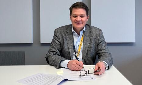
Jussi Rautee signing the Deed of Donation

Friday, February 3, 2023

A True Pioneer of ALD Research with Jeffrey Elam – ALD Stories


Tyler is joined by Dr. Jeffrey Elam from Argonne National Lab in Chicago. Jeff is the head of the Atomic Layer Deposition research program at Argonne and has received numerous awards, accolades and patents for his work, the ALD Innovator Award and Lifetime Achievement Award at Argonne as examples. 

In this episode, Tyler and Jeff discuss his time as a post doc in the Steven George lab where he built the first ALD reactors, how he began the ALD group at Argonne, and some of his award-winning work on fabricating large-area microchannel plates.

Thursday, February 2, 2023

Dutch ALD euipment leader ASM to invest $100 mil. in Korea for facility expansion

Korea’s industry ministry said Thursday it agreed with Dutch semiconductor equipment supplier ASM to boost cooperation for the firm’s planned investment of $100 million to build a production factory and a research and development center in Korea.


The two sides signed a memorandum of understanding (MOU) in Seoul on the day, which calls for joint work for the smooth implementation of the corporate investment worth $100 million through 2025, according to the Ministry of Trade, Industry and Energy.

The company is reviewing building a second factory that produces equipment for atomic layer deposition, a key process in chips manufacturing, and the expansion of its RD center in Korea.

Currently, ASM is headquartered in the city of Hwaseong, Gyeonggi Province, some 40 kilometers south of Seoul.

In October, ASM announced a plan to invest $100 million in Korea, but the amount has surged “as discussions between the two sides have developed,” a ministry official said.

Following the MOU signing ceremony, Industry Minister Lee Chang-yang and ASM CEO Benjamin Loh held a meeting for discussions on the envisioned expansion of bilateral cooperation.

“The investment is expected to help Korea better ensure stable supply chains of the sector and boost exports,” the ministry said in a release. “The government will actively extend support, such as providing incentives and resolving difficulties.” (Yonhap)


Source: Dutch chip firm ASM to invest $100 mil. in Korea for facility expansion

Wednesday, February 1, 2023

Go Go Hellzilla - the ALD Monster in Helsinki

In vacuo cluster tool for studying reaction mechanisms in atomic layer deposition and atomic layer etching processes

Journal of Vacuum Science & Technology A 41, 022401 (2023); https://doi.org/10.1116/6.0002312

ABSTRACT
In this paper, we introduce a vacuum cluster tool designed specifically for studying reaction mechanisms in atomic layer deposition (ALD) and atomic layer etching (ALE) processes. In the tool, a commercial flow-type ALD reactor is in vacuo connected to a set of UHV chambers so that versatile surface characterization is possible without breaking the vacuum environment. This way the surface composition and reaction intermediates formed during the precursor or etchant pulses can be studied in very close to true ALD and ALE processing conditions. Measurements done at each step of the deposition or etching cycle add important insights about the overall reaction mechanisms. Herein, we describe the tool and its working principles in detail and verify the equipment by presenting results on the well-known trimethyl aluminum–water process for depositing Al2O3


Asking the AI powered ChatGPT some simple questions

I have been asking the AI powered ChatGPT some simple questions - what do you think? Is there a better way to explain ALD and ALE in a simple way? I like the ALE answer more than the ALD answer.


So I reiterated and asked ChatGPT to give a very simple answer for ALD, which I like a bit more. I would probably swap electronics for semiconductor, which I did using the teaching function :-) 


Tuesday, January 17, 2023

Thermal Atomic Layer Deposition of Gold

Summary: We successfully developed the first reductive thermal ALD process for elemental gold using AuCl(PEt3) and (Me3Ge)2DHP as precursors. Highly conductive and pure gold films could be deposited at moderate temperatures of 160–180 °C. The process was proven to work on multiple substrates, although with a clear difference in nucleation that was the most favorable on a Ru surface and the least favorable on Al2O3. Furthermore, the reaction mechanism was studied and found to proceed stepwise, as expected based on the literature. The combination of high growth rate and purity of the films shows potential for many applications and furthermore proves the capabilities of the recently discovered reducing agent, (Me3Ge)2DHP.

Reductive Thermal Atomic Layer Deposition Process for Gold

Anton Vihervaara, Timo Hatanpää, Heta-Elisa Nieminen, Kenichiro Mizohata, Mykhailo Chundak, Mikko Ritala*
ACS Mater. Au 2023, XXXX, XXX, XXX-XXX
Publication Date:January 11, 2023
https://doi.org/10.1021/acsmaterialsau.2c00075


In this work, we developed an atomic layer deposition (ALD) process for gold metal thin films from chloro(triethylphosphine)gold(I) [AuCl(PEt3)] and 1,4-bis(trimethylgermyl)-1,4-dihydropyrazine [(Me3Ge)2DHP]. High purity gold films were deposited on different substrate materials at 180 °C for the first time with thermal reductive ALD. The growth rate is 1.7 Å/cycle after the film reaches full coverage. The films have a very low resistivity close to the bulk value, and a minimal amount of impurities could be detected. The reaction mechanism of the process is studied in situ with a quartz crystal microbalance and a quadrupole mass spectrometer.

Monday, January 9, 2023

Xiaomi Redmi Note 12 Pro Plus 5G use ALD coating to avoid flare and ghosting under bright light

The Note 12 Pro Plus is using Samsung’s new 1/1.4-inch HPX sensor mated to a 7P lens system with f/1.65 aperture and optical image stabilisation. Xiaomi says it is also using an atomic layer deposition (ALD) coating on this lens to minimise flare and ghosting, a common issue for smartphone cameras— including the very recent iPhones— under bright light.


The 200MP camera is paired to an 8MP ultrawide and 2MP macro. (Photo credit: Saurabh Singh/Financial Express)

Friday, December 23, 2022

Picosun initiates R&D program in Finland for sustainable semiconductor manufacturing

ESPOO, Finland, 22nd of December 2022 – Picosun, an Applied Materials company, has received funding from Business Finland to form an R&D program in the country focused on reducing the environmental impact of semiconductor manufacturing.

The four-year program, called “Chip Zero,” seeks to bring together companies across the semiconductor ecosystem in Finland with a shared mission of developing chips with zero lifetime emissions by reducing the carbon footprint of chip manufacturing and increasing the efficiency of semiconductor decarbonization applications. Picosun will initiate and lead the program with a significant grant from Business Finland. The aim is to scale the program over time with contributions from ecosystem partners to reach more than 100M€ in R&D investments.


Photo, Björn Engström, Oravais, Ostrobothnia, Finland.

Chip Zero will include efforts to reduce energy consumption and the environmental impact of chemical use in semiconductor manufacturing. Specific goals include achieving a 50-percent reduction in energy and chemical consumption of thin-film deposition and a double-digit increase in the efficiency of power electronic component applications, such as electric vehicle (EV) chargers and electric motor control electronics, by 2030. Among the strategies to achieve these goals is the development of optimized process flows for chip manufacturing.

“Picosun is excited to lead the Chip Zero program and bring together Finland’s strong technology R&D ecosystem with a common objective of developing more efficient chips and minimizing the environmental impact of manufacturing. We look forward to collaborating across the value chain to drive critical advances that will accelerate a greener and more sustainable semiconductor industry in Finland,” says Dr. Jani Kivioja, CTO of Picosun.

“With the global semiconductor market projected to reach US$1 trillion by 2030*, the need for greater efficiency in chip manufacturing is more important than ever. Finland has significant and pioneering competences in key chipmaking technologies, and the Chip Zero program intends to focus these capabilities on strengthening the country’s sustainability efforts,” continues Jussi Rautee, CEO of Picosun and Vice President of Applied Materials.

“The opportunity for technology to shape a more sustainable world has never been more promising,” says Chris Librie, Applied Materials Director of ESG, Corporate Sustainability and Reporting. “At Applied Materials, our vision is to Make Possible a Better Future, and we are pleased that our team in Finland is making a positive difference through programs like Chip Zero that aim to reduce the environmental impact of computing.”


Thursday, December 22, 2022

SparkNano's Spatial ALD tool decreases the of Iridium while increasing the production capacity of electrolyzers for green hydrogen

SparkNano's Spatial ALD tool decreases the cost and use of scarce materials like Iridium while increasing the production capacity of electrolyzers for green hydrogen.

For more detail about SparkNanos lab-to-fab product portfolio, you can download the complete spec sheet for the Labline Series here: LabLine Series — SparkNano | Spatial Atomic Layer Deposition (ALD) technology (spark-nano.com)

Technical features (12 inch system)

Substrate types flat substrates like polymer and metal foils, wafers, glass and porous substrates

Substrate size

A free envelope of 320 mm x 360 mm x 5 mm is available. In this volume any flat substrate can be placed with a substrate specific holder

Process

Both thermal and plasma enhanced s-ALD


Swedish Nanexa signs Evaluation Agreement with and issues a directed shares to Novo Nordisk for ALD based PharmaShell(R)

Nanexa AB (publ) (“Nanexa” or the “Company”) today announces that the Company has signed a Material Transfer and Feasibility Study Agreement (the “Evaluation Agreement”) with leading global pharmaceutical company Novo Nordisk A/S (”Novo Nordisk”) for the evaluation of Nanexa’s drug delivery system PharmaShell® with Novo Nordisk products. As part of the Evaluation Agreement, Nanexa will receive payments of approximately SEK 46.1 million for providing Novo Nordisk exclusivity and performing work under the Evaluation Agreement, whereof approximately SEK 41.7 million is an upfront payment at signing. In connection with the signing of the Evaluation Agreement, the board of directors of Nanexa also resolved, based on the authorisation granted by the annual general meeting held on 9 June 2022, to carry out a directed share issue to Novo Nordisk of 10,000,000 shares at a subscription price of SEK 1.72 per share (the “Directed Share Issue”) through which Nanexa raises gross proceeds of approximately SEK 17.2 million. The subscription price is equivalent to a premium of 33 percent versus the closing price yesterday for the Company’s shares. In total, Nanexa will thus receive approximately SEK 63.3 million from the Evaluation Agreement and the Directed Share Issue.


Novo Nordisk is a leading global pharmaceutical company engaged in the research, development, manufacture and commercialization of pharmaceutical products and associated devices for treatment of diabetes, obesity and other diseases. Under the Evaluation Agreement Novo Nordisk will provide Nanexa with its products and Nanexa will develop a long-acting injectable using the PharmaShell® drug delivery system. The new formulation will be evaluated in preclinical studies by Novo Nordisk. As part of the Evaluation Agreement, Nanexa receives a fee of USD 4.0 million for providing Novo Nordisk exclusivity to use PharmaShell® in combination with Novo Nordisk products, valid throughout the term of the exclusivity, and USD 0.425 million for the work performed under the Evaluation Agreement. The combined fees of USD 4.425 million correspond to approximately SEK 46.1 million. Throughout the exclusivity period Novo Nordisk has the option to negotiate a license agreement. Nanexa will be able to continue the development of its own product project (NEX-22) within the field of type 2 diabetes throughout the exclusivity period.

In connection with the signing of the Evaluation Agreement, Novo Nordisk invests SEK 17.2 million in Nanexa in the Directed Share Issue. The Directed Share Issue comprises 10,000,000 shares issued at a subscription price of SEK 1.72 per share. The subscription price is equivalent to a premium of 33 percent versus the closing price for the Company’s shares on Nasdaq First North Growth Market as per yesterday, 20 December 2022 (the “Closing Price”) and a premium of 10 percent versus the volume weighted average price of the last twenty (20) trading days for Nanexa’s shares on Nasdaq First North Growth Market preceding 20 December 2022 (the “20-day VWAP”). Following the Directed Share Issue, Novo Nordisk’s ownership in Nanexa will amount to approximately 16.5 percent of the Company’s shares and votes. The Directed Share Issue results in a dilution of approximately 16.5 percent of the Company’s shares and votes. The number of shares of Nanexa after the Directed Share Issue will amount to 60,695,626 and the share capital of Nanexa will increase by approximately SEK 1,294,213.58 to approximately SEK 7,855,310.32. Additionally, Novo Nordisk undertakes as part of the Directed Share Issue to subscribe for its pro-rata portion of any future rights issue conducted prior to 31 December 2023 up to a maximum of USD 2.0 million. The undertaking is conditional on certain terms being met.

The net proceeds from the Directed Share Issue will primarily be used to strengthen the Company’s financial position, and to enable planned preclinical and clinical studies as well as other value creating activities supporting PharmaShell® and the NEX projects.


The purpose of the Directed Share Issue, and the reason for deviation from the preferential rights of the shareholders, is (i) in a time and cost efficient manner acquire capital and to finance the joint development project between the Company and Novo Nordisk pursuant to the Evaluation Agreement , (ii) to add a strategically important and financially strong shareholder, who wishes to participate in the future development of the Company, to its shareholder base, (iii) that Novo Nordisk will bring valuable industry and sector knowledge to the Company, and (iv) that a rights issue, as opposed to a directed issue, would not ensure that Novo Nordisk actually becomes a shareholder in the event that the rights issue is fully subscribed. The board further believes that it would entail a risk that the Company cannot accommodate the capital needs associated with its business plan at favourable terms in the current market situation. Consequently, the overall assessment of the Board of Directors is that the reasons for carrying out the Directed Share Issue in this way, in this specific case, outweigh the reasons justifying the main rule of issuing shares with preferential rights for existing shareholders, and that a new issue with deviation from the shareholders' pre-emption rights is therefore in the interests of the Company and all shareholders.

The subscription price has been determined through arm's length negotiations between the Company and Novo Nordisk. The subscription price exceeds the Closing Price by 33 percent and the 20-day VWAP by 10 percent. Existing shareholders have therefore had good opportunities to acquire shares on similar or more favourable terms recently. As the subscription price in the Directed Share Issue not insignificantly exceeds both the closing price and the 20-day VWAP, the board of directors considers that it has been ensured that the subscription price is on market terms.

Göran Ando, Chairman of the board, comments:

"I am very pleased that we through the Evaluation agreement and the Directed Share Issue can give Nanexa good conditions to continue developing the Company into a world leading drug development company for long-acting injectables, based on our unique PharmaShell® technology. The collaboration with Novo Nordisk further strengthens Nanexa’s portfolio of partner projects with a good opportunity to develop into a more extensive development program and long-term license agreement. The deviation from the shareholders' pre-emptive rights is not a decision taken lightly, but the possibility to reach a solution under prevailing volatile market conditions with a premium, as well as adding Novo Nordisk as strategic partner, was a strong reason."

Monday, December 19, 2022

Foundations of atomic-level plasma processing in nanoelectronics (Open Access)

Foundations of atomic-level plasma processing in nanoelectronics

Karsten Arts, Satoshi Hamaguchi, Tomoko Ito, Kazuhiro Karahashi, Harm C M Knoops, Adriaan J M Mackus and Wilhelmus M M (Erwin) Kessels
Plasma Sources Sci. Technol. 31 103002 OPEN ACCESS  

This article discusses key elementary surface-reaction processes in state-of-the-art plasma etching and deposition relevant to nanoelectronic device fabrication and presents a concise guide to the forefront of research on plasma-enhanced atomic layer etching (PE-ALE) and plasma-enhanced atomic layer deposition (PE-ALD). As the critical dimensions of semiconductor devices approach the atomic scale, atomic-level precision is required in plasma processing. The development of advanced plasma processes with such accuracy necessitates an in-depth understanding of the surface reaction mechanisms. With this in mind, we first review the basics of reactive ion etching (RIE) and high-aspect-ratio (HAR) etching and we elaborate on the methods of PE-ALE and PE-ALD as surface-controlled processing, as opposed to the conventional flux-controlled processing such as RIE and chemical vapor deposition (CVD). Second, we discuss the surface reaction mechanisms of PE-ALE and PE-ALD and the roles played by incident ions and radicals in their reactions. More specifically, we discuss the role of transport of ions and radicals, including their surface reaction probabilities and ion-energy-dependent threshold effects in processing over HAR features such as deep holes and trenches.


Examples of applications of PE-ALD in patterning, logic device fabrication, and memory device fabrication. The layers prepared by PE-ALD are indicated in (dark) red. In these examples, i.e., self-aligned quadruple patterning (A), gap-filling (B), and dielectric lining (C, left), the film conformality, thickness control, and material quality provided by PE-ALD are essentia

Thin layers paved the way for ASMI’s success - Outgoing CTO Ivo Raaijmakers explains what atomic layer deposition has brought the semiconductor industry

ASM International played a key role in developing a deposition technique that has saved Moore’s law more than once. Outgoing CTO Ivo Raaijmakers explains what atomic layer deposition has brought the semiconductor industry – and ASMI – and what more is in store.
This vision has come true. The technique that ASMI acquired through Microchemistry – atomic layer deposition (ALD) – has become an integral part of the semiconductor manufacturing process. And that’s just the beginning, according to Raaijmakers. The demands placed on material layers are ever higher – thinner, more uniform, featuring just the right properties – and ALD is the best technique to meet them, the former CTO argues.


Well before ALD had proven itself in the deposition of high-k materials, Raaijmakers was already looking at which applications would follow. On his initiative, ASMI acquired Korean company Genitech in 2004, a specialist in plasma-enhanced ALD technology (PEALD). Plasmas are more reactive than un-ionized gases and therefore can deposit materials at lower temperatures. Because chipmakers often have to deal with strict temperature budgets, PEALD expands the scope of ALD.

Saturday, December 17, 2022

ALD Stories Podcasts by Tyler Myers

Message from Tyler Myers to the ALD-Community - The community with a forecasted 5-Year CAGR 20.5% (2022-2026) - Please consider following the ALD Stories podcast! Each month, you'll find insightful interviews about the lives and research of the best folks in ALD. We already have a couple episodes ready to go for 2023!


Here is how I listen to the ALD Stories using my new Sony Head set with 2 processors and 8 microphones for unprecedented noise cancellation and exceptional call and sound quality. Besides that my phone has so many ALD-chips I sort of bet that each chip in the headphones has ALD in them so what better way to deploy ALD technology than to run and listen to ALD Stories using 8 microphones and the advanced speakers to filter out the wind, ugly birds song and traffic and still be able to answer and participate in web meetings?


2023 I will experiment with adding video feed capability.


Kokusai Electric relies on patterned 3D substrates in thin film process metrology from Chipmetrics

Kokusai Electric is one of the leading semiconductor thin film process equipment manufacturers in the world. Recently, in the context of Japan Society of Applied Physics 69th Spring Meeting 2022, Kokusai presented their advanced thin film measurement and analysis concept used in their semiconductor process development.

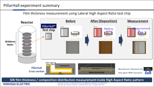
The concept focuses on film thickness and localized film composition measurements from the special designed 3D patterned substrates, where the patterns are fine high aspect ratio structures.

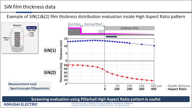
The average film thickness is obtained indirectly by measuring the mass change in the special 3D patterned wafer before and after the film depositions. The thickness accuracy is further improved by taking into account the high aspect ratio and wafer level non-uniformity measured by PillarHall® Lateral High Aspect Ratio (LHAR) test chips positioned on the carrier wafer. The PillarHall® measurement, enables easy screening after peeling off the top roof membrane and by measuring the film thickness distribution and conformality by the ellipsometer line-scanning measurements.

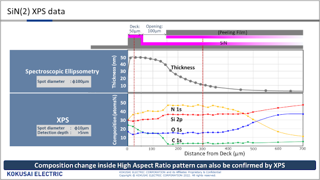
PillarHall® LHAR test chip has also another important function in Kokusai’s analysis concept. Namely, it is used for film elemental composition characterization along the trench wall in high aspect ratio structure. The measurement is carried out as a line-scan by XPS or SEM-EDS. For example, the characterization showed that two kinds of SiN processes behaved differently and Si/N composition changes along the high aspect ratio (AR>1000) trench were observed.


Figure 1. PillarHall experiment summary


Figure 2. SiN film thickness data


Figure 3. SiN(2) XPS data

Figures 1-3 show the PillarHall experimental set-up, data from the film thickness penetration depth profiles and XPS composition data of two kind of Kokusai’s SiN processes, SiN (1) and SiN (2).

Kenji Kameda and Akane Kitamura from Metrology Team, Kokusai Electric emphasized that:” It is difficult to obtain the analysis of thin films on high aspect ratio patterns without cross-sectional TEM. PillarHall is a simple and effective tool, it has fine patterns, and it enables us to use XPS and ellipsometer instead of TEM. Therefore, PillarHall is useful as an efficient measurement tool to improve Kokusai’s film forming technology.”

PillarHall LHAR test chip is a product of Chipmetrics Ltd, Finland. Chipmetrics CEO Dr. Mikko Utriainen reminds that any PillarHall data can be published without confidentiality concerns and the results are also well comparable between reactor systems and processes. The openness and accuracy of the ALD conformality data was one of the reasons why pioneering ALD scientists in Finland started to develop the PillarHall concept already in 2013.

Kokusai’s example shows that PillarHall is an efficient measurement tool and help to improve film forming technology for advanced semiconductor processes.

PillarHall is a product of Chipmetrics Ltd. Contact: info@chipmetrics, www.chipmetrics.com

Friday, December 16, 2022

MIT.nano adds new instruments to create and analyze at the nanoscale from Arradiance

The Arradiance GEMStar XT-DP plasma-enhanced atomic layer deposition (ALD) system was installed at MIT.nano in May.


The system is dedicated specifically to deposit high-quality nanometer-scale thin oxide films including aluminum oxide, hafnium oxide, zirconium dioxide, and silicon dioxide. The Arradiance ALD can be used for samples ranging from small pieces up to 200-mm wafers and has a load lock that isolates the deposition chamber from the user, allowing for better contamination control.


Friday, November 25, 2022

Applied Materials Delivers Strong FY 2022 Numbers including Picosun ALD

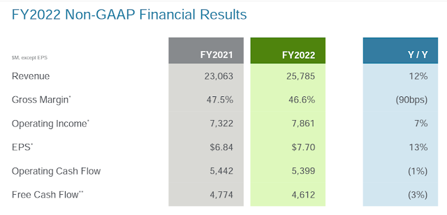
Semiconductor equipment maker Applied Materials has reported strong earnings for FY 2022 (ended October 30). Total sales revenue increased 12% YoY to $25.78 billion despite supply chain shortages, geopolitical and macroeconomic headwinds, and softening consumer demand.

LINK: https://ir.appliedmaterials.com/

The company’s uniquely enabling technology and growing installed base will be its key growth drivers as chipmakers accelerate ramping up of new process nodes in R&D for high-volume manufacturing.


Key developments in FY 2022
  • Applied Materials acquired Picosun, a Finland-based innovator in atomic layer deposition (ALD) technology. This acquisition broadens Applied’s product portfolio and puts it in a great position to capture a large portion of the specialty semiconductor market in the coming years.
  • Collaboration with the Institute of Microelectronics (IME), a research institute under Singapore’s Agency for Science, Technology and Research (A*STAR). IME’s strategic R&D capabilities complement well Applied’s expertise in advanced packaging solutions and will accelerate material, equipment and process technology solutions for hybrid bonding and other emerging, 3D chip integration technologies.
  • Introduced new Ioniq™ PVD system to solve wiring resistance challenges of 2D scaling. This new integrated solution offers a significant reduction in electrical resistance, which has become a critical bottleneck to further improvements in chip performance and power.
Financial highlights
  • Semiconductor Systems revenue increased 15% YoY in FY 2022 to $18,797 million on account of strong orders as customers continued to invest in next-generation technology.
  • Applied Materials’ service revenue increased 11% YoY in FY 2022 to $5,543 million, accounting for 21% of the annual net revenue.
  • Display and Adjacent Markets revenue decreased 19% YoY in FY 2022 to $ 1,331 million.
  • Non-GAAP gross margin was at 46.6% in FY 2022.
  • Non-GAAP operating profit grew by over 7% to $7.86 billion.
  • Non-GAAP EPS increased nearly 13% to $7.70.
  • Total ending backlog increased 62% to $19 billion with Semiconductor Systems backlog increasing 90% to nearly $12.7 billion and services backlog increasing 30% to over $5.6 billion.
  • The company generated about $5.4 billion in operating cash flow and over $4.6 billion in free cash flow.
  • The company’s installed base grew 8% YoY in FY 2022.
  • The number of tools under comprehensive, long-term service contracts grew 16% YoY with the over 90% renewal rate for these agreements demonstrating the value customers see in subscription services.
  • New export regulations for US semiconductor technology sold in China reduced Semiconductor Systems and AGS fourth quarter revenue by approximately $280 million.

Tuesday, November 8, 2022

Recent ALD news on shared on Twitter #ALDep

SparkNano Raises EUR 5.5M to Scale Spatial Atomic Layer Deposition for Energy Applications in a round led by ALIAD Venture Capital by Air Liquide

SparkNano Raises EUR 5.5M to Scale Spatial Atomic Layer Deposition for Energy Applications in a round led by ALIAD Venture Capital by Air Liquide.

SparkNano - LINK (linkmagazine.nl)


Friday, November 4, 2022

ALD coatings for next-generation solar cells

(Helsinki : LINK) Researchers at the University of Helsinki are developing thin films needed in new types of halide perovskite solar cells, and matching ALD processes, in order to provide increasingly affordable solar cells, enable their integration into objects and, consequently, promote the transition to renewable energy.

The 2022 Millennium Technology Prize has been awarded today October 25 to Scientia Professor Martin Green of the UNSW Sydney, Australia, for his innovation that has transformed the production of solar energy.


Members of the research group next to the ALD reactor. Georgi Popov (left), Marianna Kemell, Alexander Weiss and Mariia Terletskaia. (Image: Riitta-Leena Inki)

Most commercial solar cells are silicon-based, and apply PERC (Passivated Emitter and Rear Cell) technology originally launched in 1983 by Martin Green, a recently awarded Millennium Award. However, increasingly efficient, inexpensive and durable solar cells are being developed all over the world. Even in the case of silicon-based cells, a transition is underway to novel techniques, including the tunnel oxide passivated contacts (TOPCon) concept, where several layers of silicon and oxide are added to the cell.

Transparent and flexible solar cells
In addition to silicon, other solar cell technologies are being investigated. The most promising new technique is based on the use of halide perovskites as a light-absorbing material. The general chemical formula of halide perovskites is ABX₃, where A is an alkali metal or an amine, B is tin or lead, and X is a halide. The most commonly studied compound is methylammonium lead iodide CH₃NH₃PbI₃. Perovskite solar cells are on the verge of commercialisation, and some manufacturers believe they will be mainstream in a couple of decades.

“As these new types of solar cells can be transparent, they can be installed in, for example, windows. They are also flexible, which increases their uses,” says Senior University Lecturer Marianna Kemell, who heads the research project funded by the Academy of Finland.

Even though halide perovskite solar cells have achieved high efficiency levels, problems with cell stability and the lack of industrial-scale production techniques have constituted bottlenecks impeding their widespread adoption.

A breakthrough with metal iodides
While pursuing a master’s degree in chemistry, Doctoral Researcher Georgi Popov boldly chose halide perovskites and their atomic layer deposition (ALD) as the topic of his master’s thesis. There were doubters, as prior research-based knowledge was scarce.

“We identified suitable chemicals and were able to design a reaction that enabled us to create a metal iodide coating through deposition for the first time. We were able to demonstrate that this can actually be done through atomic layer deposition. The first successful trial was carried out with lead iodide, which was then processed into CCH₃NH₃PbI₃ perovskite through a further reaction,” Popov says. “The research article was published in the refereed Chemistry of Materials scholarly journal. Later on, we also developed ALD processes for caesium iodide and CsPbI₃ perovskite.”

Coatings produced through atomic layer deposition are used in roughly 30% of silicon-based solar panels. The ALD group headed by Professor Mikko Ritala at the University of Helsinki has achieved promising results in terms of the technique’s adaptability to perovskite solar cells. The advantage of coatings produced by atomic layer deposition is that they form a uniform and comprehensive layer even on rough surfaces.

“If at some point we start making tandem solar cells, which combine a silicon cell and a perovskite cell, we know how to make that perovskite. We are developing the recipes and the chemistry used to grow perovskite,” Popov says.

While the work currently being carried out is basic research, developing recipes and experimenting with small surface areas, the technique is applicable to large-scale production.

“The current plants manufacturing solar cells in China and elsewhere are able to adjust their equipment to produce ALD-coated solar cells,” says Popov.

The future of solar cells
More than 80% of solar cells are manufactured in China, where industrial-scale ALD devices are also produced. Wei-Min Li, PhD, an alum of the University of Helsinki’s Department of Chemistry, works as the chief technology officer at Leadmicro, a leading Chinese manufacturer of ALD equipment. This connection gives the department a solid grasp on where the field is going. ALD equipment used to produce silicon-based solar panels can also be expanded to produce next-generation solar cell materials.

“We are developing the future technical solutions that will gradually replace and supplement current production. In the future, fewer resources will be needed for production, and, thanks to increasingly effective cells, less surface area as well. When solar cells can be installed on uneven surfaces in addition to even ones, we no longer need to build solar parks in fields, as fields are needed for other purposes,” Popov notes.

However, Popov points out that we cannot afford to wait for new technical solutions, as the utilisation of renewable energy sources must be increased now. By replacing current sources of energy with solar or wind power as much as possible, pressure will increase and the entire field will advance.

“The best part of silicon-based cells is that they last roughly 20 to 30 years and will continue to function even after that, albeit possibly less efficiently. Since solar cells produced with the PERC technique are the current state of the art, and they are available, it is advisable to acquire as many of them as possible. They will pay for themselves,” Senior University Lecturer Kemell says.

The project entitled ‘Atomic Layer Deposition as key enabler of scalable and stable perovskite solar cells’, which is funded by the Academy of Finland, will continue until 2024. In addition to Marianna Kemell and Georgi Popov, contributing to the project are Doctoral Researcher Alexander Weiss and master’s student Mariia Terletskaia.

Samsung use NCD ALD for wirebonding alternatives to expensive Gold

According to a recent article by TheElec, Samsung has developed a new chip packaging technology with its key partners for automotive chips. The company employs an aluminum oxide (Al2O3) coating bonding wire technology with improved reliability and insulation compared to previous bonding wires.

Bonding wires connect the I/Os with the lead frame or printed circuit boards. Most of them in the past have been made with gold (Au) as they are flexible and conductive. But as gold prices continue to rise, many companies attempt to mix them with silver (Ag) or copper (Cu). However,  these mixed materials usually have weak adhesiveness with their coating materials. This is unacceptable for chips aimed at automobiles as they are exposed to high-temperature and high-humidity environments.

Samsung’s aluminum alternative, which it is developing with Electron, NCD and LT Metal, doesn’t have this weakness since the aluminum oxide is coated at nanometer thinness onto the metal used as wire. Aluminum oxide bonds well with insulating coating materials that use epoxy. The precursors used to coat the aluminum oxide such as tri-metal aluminum (TMA) are also relatively cheap and used in HVM since a long time.


Insulated, Passivated & Adhesively-Promoted Bond WireUsing All-in-One Al2O3 Coating

Soojae Park(1), Jonghyun Lee(1), Chulhyung Cho(1), Namhoon Kim(1), Yongje Lee(1), Sichun Seo(1), Manho Kim(1), Youngkwon Yoon(1), EulgiMin(2), Kyujung Choi(2), Sang-Hoon Lee(3) Hong-Sik Nam(3),Monghyun Cho(4) & Jeongtak Moon(4),(1)Samsung Electronics Company130 Samsung-Ro, Yungtong-Gu, Suwon-Si, Gyunggi-Do, Republic of Korea(2)NCD Co., Ltd.(3)LT Metal, Ltd.(4)MK Electron Co., Ltd. (2) (PDF) Insulated, Passivated & Adhesively-Promoted Bond Wire Using All-in-One Al2O3 Coating. Available from:

University of Erlangen demonstrate sALD of Crystalline Metal–Organic Framework Thin Films (MOFs)

For the first time, a procedure has been established for the growth of surface-anchored metal–organic framework (SURMOF) copper(II) benzene-1,4-dicarboxylate (Cu-BDC) thin films of thickness control with single molecule accuracy. For this, we exploit the novel method solution atomic layer deposition (sALD). The sALD growth rate has been determined at 4.5 Å per cycle. The compact and dense SURMOF films grown at room temperature by sALD possess a vastly superior film thickness uniformity than those deposited by conventional solution-based techniques, such as dipping and spraying while featuring clear crystallinity from 100 nm thickness. The highly controlled layer-by-layer growth mechanism of sALD proves crucial to prevent unwanted side reactions such as Ostwald ripening or detrimental island growth, ensuring continuous Cu-BDC film coverage. This successful demonstration of sALD-grown compact continuous Cu-BDC SURMOF films is a paradigm change and provides a key advancement enabling a multitude of applications that require continuous and ultrathin coatings while maintaining tight film thickness specifications, which were previously unattainable with conventional solution-based growth methods.

Solution Atomic Layer Deposition of Smooth, Continuous, Crystalline Metal–Organic Framework Thin Films

Maïssa K. S. Barr*, Soheila Nadiri, Dong-Hui Chen, Peter G. Weidler, Sebastian Bochmann, Helmut Baumgart, Julien Bachmann, and Engelbert Redel*
Chem. Mater. 2022, XXXX, XXX, XXX-XXX
Publication Date:November 2, 2022
https://doi.org/10.1021/acs.chemmater.2c01102


Monday, October 10, 2022

Samco launches new ICP Tornado Plasma ALD system

Samco, a leading manufacturer of etching, deposition and surface treatment processing equipment for the semiconductor and related industries and academic facilities, launches the new Plasma Enhanced Atomic Layer Deposition (PEALD) system, "AD-800LP". The main target of the system is gate oxide film deposition for next-generation power devices of silicon carbide (SiC) and gallium nitride (GaN) materials, which will play important role toward carbon neutral.


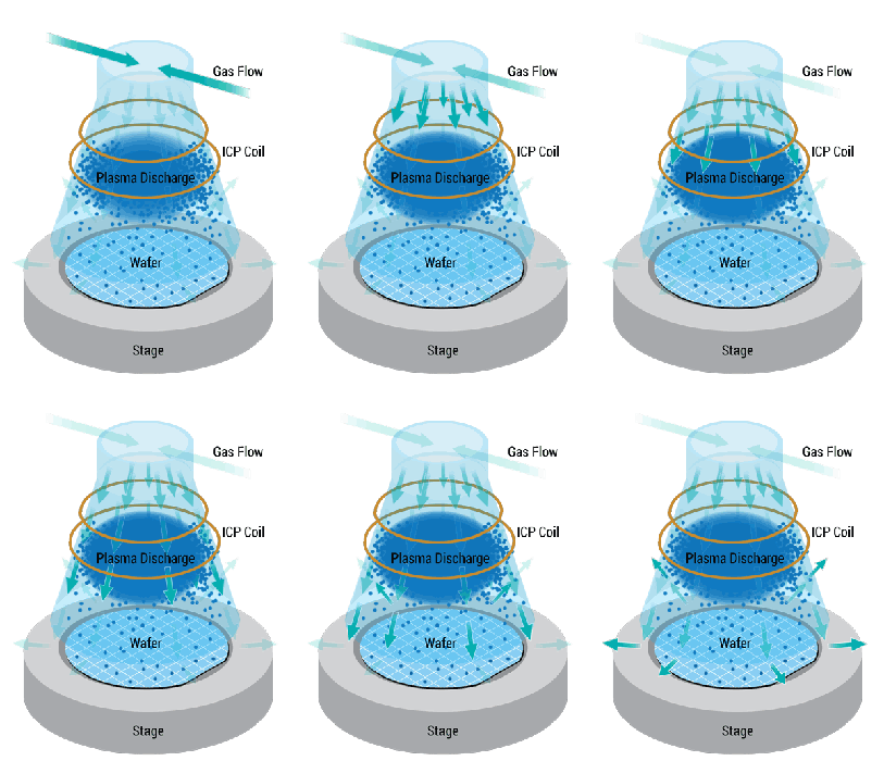
Tornado ICP Coil®,  Samco ICP etch systems are equipped with Tornado ICP Coil® which was specially designed for compound semiconductor etching. It is difficult to achieve desired profiles of InP and GaAs due to byproduct redeposition. The Tornado ICP Coil® reduces byproduct redeposition by optimizing etchant species and densities in plasma etching. (Source: Samco)

The plasma enhanced ALD system "AD-800LP" is a multi-purpose R&D system equipped with a unique ICP plasma source called "Tornado ICP", in addition to the conventional thermal ALD capability. AD-800LP enables various film deposition such as oxide or nitride films by Tornado ICP, which is Samco's proprietary plasma technology and is different from remote plasma. Tornado ICP enables stable plasma discharge even in the high-pressure range during ALD deposition.

“We are also considering a cluster ALD system that can connect multiple reaction chambers for production” says Tsukasa Kawabe, President and COO of Samco. “The launch of the AD-800LP will greatly enhance our presence in the world ALD equipment market.” Tsukasa adds.

As a global mid-sized company, Samco has successfully delivered numerous dry etch systems and plasma enhanced CVD systems for the electronic device field, mainly for compound semiconductors such as SiC, GaN, and GaAs, not only in Japan but also in the United States, Europe, Taiwan, Korea, China, Southeast Asia, India, and other countries.

The new Research Center for Nano Thin Films & Materials, which opened in February 2022, conducts research and development of unique thin film deposition, including ALD system. Samco will continue to utilize our "thin-film technology" to develop unique products and expand sales globally.

About Samco Inc.
Samco Inc. (TSE: 6387) stands for Semiconductor And Materials Company, and is a leading manufacturer of processing equipment for the semiconductor and related industries founded by Mr. Osamu Tsuji in Kyoto, Japan in 1979. Over the past forty-three years, more than 4,300 Samco systems have been installed and used in 35 different countries. Its equipment and thin film technology are widely adopted in the fabrication of semiconductor devices, including BAW filters, SiC power devices, GaN RF devices, GaAs VCSELs, InP lasers, microLEDs, MEMS, TSVs, advanced packaging, and so on. Learn more at https://www.samcointl.com/.

NCD’s ALD technology and equipment for oxidation barrier of copper-based substrates

Copper is a metal used widely as the main material of Printed Circuit Board (PCB) and Lead Frame. But it is required to protect the oxidation because copper is easily oxidized in the condition of humidity, temperature, and pH, etc.

Electroless Nickel Immersion Gold (ENIG), Organic Solderability Preservative (OSP), Immersion Sn or Ag (ImSn or ImAg) is generally used to prevent oxidation of opened copper area after Solder Masking in PCBs. The lead Frame is protected from oxidizing by plating Au, Ag, Pd, and Ni after Lead Frame forming.

Recently, many groups have studied about preventing oxidation on the surface of copper by various corrosion protection layers of ALD metal oxides. Especially, Appling Al2O3 layer to the oxidation barrier is actively being researched.


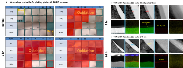
 < Surface images and TEM & EDS of Cu plates coated by ALD thin films after annealing test >

After depositing Al2O3 layers on Cu-plated plates with various film thicknesses and process temperatures, the oxidation and corrosion behavior of the coated copper was examined with different annealing times in the oven. There was no oxidation before annealing, but after annealing for 1hr, as the sample’s thickness lowered and process temperature decreased, the oxidation happened and increased gradually. There was no oxidation on the plates coated with 50~60 ALD cycles and at process temperatures of 70~100 after annealing for 5hr, and oxidation didn’t occur only in the case of 60 cycles and 100 after annealing for 24hr.

To analyze the change of the structure and confirm the oxidation behavior, TEM and EDS were measured on 5 and 10nm Al2O3 coated Cu plates at 100. The results showed that a thick Cu oxide layer was built by combining Cu coming out through the 5nm Al2O3 layer and outer oxygen after annealing.

On the other side, in the case of depositing 10nm Al2O3 film, the ALD layer was maintained after annealing, so Cu oxide layer wasn’t built on the surface. Therefore it confirmed that 10nm ALD Al2O3 layer showed an excellent corrosion barrier.


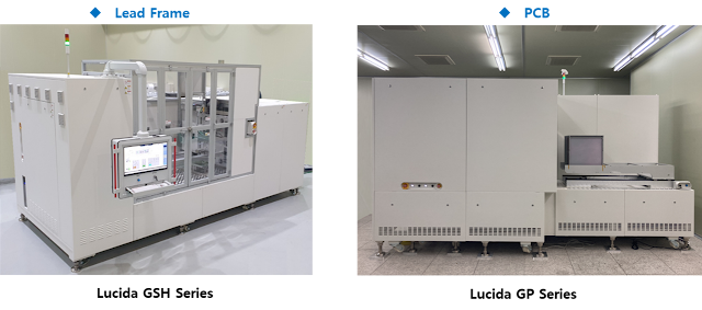
< ALD equipment for Lead Frame and PCB >

Copper-based PCBs and Lead Frames for semiconductors may have great properties to prevent humidity and oxygen by ALD-coated corrosion barriers.    

NCD has high volume and large area ALD equipment and technology for this kind of application. ALD tools for Lead Frames could be used by adding a dedicated transfer module on the base of Lucida GSH Series. And NCD has been developing new ALD equipment, Lucida GP Series, for large and flexible PCB substrates. NCD would extend the new ALD application area continuously through constant R&D.

Source: http://www.ncdtech.co.kr/2018/bbs/board.php?bo_table=eng_board_05&wr_id=57


Wednesday, October 5, 2022

Ascent Funds Invests in Forge Nano Atomic Armor for Lithium-Ion Batteries & Hydrogen Fuel Cells

September 13, 2022; Miami, USA: Ascent Funds (“Ascent”), an energy-tech venture company today announced it has invested in Forge Nano Inc (“Forge Nano”), inventor of nanocoating technology Atomic Armor, which coats a protective atomic layer on a wide range of materials, powders and products to deliver greater performance for a lower cost. Forge Nano is preparing to build a US$120 million 500MWh Atomic Armor battery facility in Denver, Colorado which will deliver some of the most efficient and longest lasting batteries in the world.


Batteries that have Atomic Armor; last 100% longer, charge 300% faster

Forge Nano is the global leader in scalable atomic layer deposition (“ALD”), a unique coating technology that produces a protective atomic layer on a range of materials, powders, and products providing greater protection, performance, durability and safety.

Invented in the 1960s, ALD is mainly used in the semiconductor and OLED industries with the technology commonly found in many mobile phone components. Since 2011, Forge Nano has developed a proprietary ALD process that allows for four times faster coating speeds than any other semiconductor ALD tool provider and enables scale for use on powders and larger surface area objects, such as; lithium-ion batteries, hydrogen fuel cells, pharmaceuticals and vaccines, consumer, sporting and apparel products. Forge Nano calls their ALD coating Atomic Armor.

Atomic Armor works especially well for battery materials, where it stabilizes the surfaces at the atomic level. These coatings prevent excessive wear and damage to the batteries by preventing unwanted reactions among the battery’s internal components. Batteries that have Atomic Armor last 100% longer, charge 300% faster, and dissipate heat more effectively.

Over the past decade, Forge Nano has emerged as a market leader in large-scale ALD. In 2021, Forge Nano announced the world’s first ALD enabled battery for space, with the launching of a high energy lithium-ion battery into orbit aboard the SpaceX Transporter-2 rideshare mission. The Li-ion batteries, featuring Forge Nano Particle ALD technology and Enersys Zero Volt Technology were integrated into spire Global, Inc’s LEMUR-2 satellite.

Atomic Armor can improve performance in hydrogen fuel cells, electrolyzers and storage

Since 2019, Forge Nano has collaborated with the U.S Department of Energy’s National Renewable Energy Laboratory, University of Connecticut, Colorado School of Mines and Fraunhofer Institute of Solar Energy Systems in Germany to accelerate the development of more efficient component parts for hydrogen fuel cells, electrolyzers and hydrogen storage technology. In the hydrogen value chain, Forge Nano’s Atomic Armor can transition fuel cells away from low-scale, costly electrode fabrications while increasing durability and limiting the use of platinum group metals. This reduces both the cost of the fuel cell as well as the technology’s dependence on expensive metals.

Mr David Wu, President of Ascent Funds said, “At Ascent, we look for transformational technology that can have an immediate and profound impact on the energy transition, especially in the hydrogen ecosystem. With over a decade’s experience in enhancing lithium-ion batteries and other materials, Forge Nano is the only commercially large-scale ALD player that can offer a real step-change in productivity, performance and cost for hydrogen companies. For example, instead of using expensive platinum or titanium catalysts, fuel cells could use low cost metal catalysts coated with atomic armor. Until now, atomic armor for hydrogen technology was a theoretical ambition because it couldn’t be scaled – today, atomic armor is a reality’.

Mr. Paul Lichty, CEO of Forge Nano, said: “We are excited to have Ascent join us as investors and advisors. They have a strong track record in identifying game changing technologies and helping those companies to scale and commercialize. In addition, Ascent’s knowledge and experience across the global hydrogen industry will be paramount as our technology becomes an accelerant in the energy transition, particularly for mobility, be it BEV or FCEV.”

Ascent joins existing shareholders Volkswagens, LG Chem, Air-Liquide, Mitsui Kinzoku, Sumitomo and SCG from Thailand.

Tuesday, October 4, 2022

ASM International has completed the acquisition of Italian Silicon Carbide Equipment Manufacturer LPE S.p.A.

ASM International (Euronext Amsterdam: ASM) today announces that it has completed the acquisition of LPE S.p.A., after having received regulatory approvals.

On July 18, 2022, ASM entered into a definitive agreement under which it would at closing acquire all of the outstanding shares of LPE, an Italian based manufacturer of epitaxial reactors for silicon carbide (SiC) and silicon. As announced in our press release of July 18, 2022, the transaction is financed with a combination of cash, a conditional earn out, and 631,154 ASM shares (a combination of 580,000 treasury shares and 51,154 newly issued shares).


The acquisition has been completed today, and LPE is now a fully owned subsidiary and will operate as a product unit under ASM’s Global Products organization.

“This is an important milestone for ASM. We are excited to welcome LPE and its talented and experienced team into ASM,” said Benjamin Loh, President and CEO of ASM. “Together with LPE we look forward to capturing many of the opportunities in the high-growth silicon carbide epitaxy market and to support our power electronics customers with innovative solutions, driving the further electrification of the automotive industry.”
“I believe ASM is the right partner for LPE, especially now looking at the growth we are seeing in the silicon carbide market. The global reach that ASM has with its entrenched supplier and customer networks will bring benefits to all stakeholders,” said Franco Preti, who envisioned the silicon carbide opportunity in the earliest stages and led LPE growth as CEO until the acquisition.

LPE is profitable with margins in line with ASM’s 2021-2025 target model. As announced earlier, LPE’s revenue is projected to grow to more than €100 million in 2023, mainly driven by its SiC epitaxy equipment business. Based on ASM internal estimates, demand for SiC epitaxy equipment is forecasted to grow at a CAGR in excess of 25% from 2021 to 2025, driven by the rapidly expanding market for electric vehicles.