Showing posts with label MOCVD. Show all posts

Friday, November 24, 2023

AIXTRON Launches €100 Million Innovation Center to Boost Semiconductor Technology Development

AIXTRON SE, a leader in deposition equipment for the semiconductor industry, has begun constructing a new EUR 100 million innovation center at its headquarters in Herzogenrath, Germany. This significant investment will establish a 1000m2 cleanroom, along with space for metrology equipment, incorporating cutting-edge industry technologies. Scheduled for initial use in the second half of 2024 and official handover in early 2025, this facility marks a major milestone in AIXTRON's 40-year history. The innovation center, celebrated during a ground-breaking ceremony attended by political, scientific, and industry representatives, reinforces AIXTRON’s commitment to leading semiconductor technology and future growth. 

Dr. Felix Grawert, CEO of AIXTRON, highlighted the center's role in developing next-generation solutions for digitalization, electromobility, and energy efficiency. The cleanroom, classified as ISO 6 with potential expansion to ISO 4, is designed for high efficiency, utilizing a compact, multi-level layout to maximize space and streamline processes.


About AIXTRON

AIXTRON SE is a leading provider of deposition equipment to the semiconductor industry. The Company was founded in 1983 and is headquartered in Herzogenrath (near Aachen), Germany, with subsidiaries and sales offices in Asia, United States and in Europe. AIXTRON´s technology solutions are used by a diverse range of customers worldwide to build advanced components for electronic and optoelectronic applications based on compound or organic semiconductor materials. Such components are used in a broad range of innovative applications, technologies and industries. These include Laser and LED applications, display technologies, data transmission, SiC and GaN power management and conversion, communication, signaling and lighting as well as a range of other leading-edge applications.

Our registered trademarks: AIXACT®, AIXTRON®, Atomic Level SolutionS®, Close Coupled Showerhead®, CRIUS®, Gas Foil Rotation®, OVPD®, Planetary Reactor®, PVPD®, TriJet®

For further information on AIXTRON (FSE: AIXA, ISIN DE000A0WMPJ6) please visit our website at www.aixtron.com

Thursday, November 16, 2023

Aixtron Reports Strong Revenue Growth and Doubled Profits in Q3 2023, Driven by High Demand for GaN and SiC Power Electronics

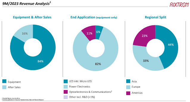
 In Q3 2023, Aixtron SE, a deposition equipment maker based in Herzogenrath, Germany, reported a revenue of €165 million, marking an 86% increase from the previous year but a 4.9% decrease from the last quarter. The company's revenue for the first nine months of 2023 rose by 49% year-on-year to €415.7 million, predominantly from equipment sales.


A significant portion of the revenue came from the sale of metal-organic chemical vapor deposition (MOCVD)/chemical vapor deposition (CVD) systems for manufacturing gallium nitride (GaN) and silicon carbide (SiC) based power electronics, which accounted for 82% of equipment revenue. There was a notable shift from optoelectronics and LED systems to SiC and GaN-based systems.

Regionally, Asia contributed 44% of the revenue, followed by Europe (33%) and the Americas (23%). The gross margin improved to 46% in Q3 from 42% in Q2, with operating profit doubling year-on-year due to a better product mix.

However, the company faced increased operating expenses, primarily due to a 44% rise in R&D costs. This led to a significant drop in free cash flow, mainly attributed to a rise in inventories in anticipation of higher business volumes.

Aixtron launched the G10-GaN system, an addition to its G10 product line, which is expected to generate over 50% of its total GaN revenues in 2024. Despite a dip in order intake in Q3, Aixtron projects a higher intake in Q4 and confirms increased full-year growth guidance, expecting continued strong demand, especially for efficient power electronics.

The company is also investing in a new Innovation Center to expand its R&D capabilities, aligning with global trends in electrification, digitalization, and renewable energies, where materials like SiC and GaN are becoming mainstream.

Source: 

Aixtron’s Q3 Revenue And Earnings Up Significantly Year-on-year - Plato Data Intelligence (zephyrnet.com)

Tuesday, September 19, 2023

AIXTRON's MOCVD Machine Advancing 2D-Materials at imec

AIXTRON, a German semiconductor equipment manufacturer, has successfully installed the CCS 2D Metal-Organic Chemical Vapour Deposition (MOCVD) reactor at the Interuniversitair Micro-Electronica Centrum (imec) in Belgium. Part of the 2D Experimental Pilot Line initiative, this reactor facilitates large-scale epitaxial deposition of 2D-materials on 200/300 mm wafers, marking a significant milestone in the transition of these materials from lab to fab.

Inge Asselberghs, Director of the 2D Experimental Pilot Line at imec, emphasizes the unique position of imec as a bridge between academia and industry, offering access to both fundamental research laboratories and industrial infrastructure.

Salim El Kazzi, 2D Product Manager at AIXTRON, outlines the challenges of the lab-to-fab transition, including miscommunication and the technical intricacies of 2D-materials. AIXTRON addresses these challenges by fostering collaboration among top researchers and providing FAB-compatible reactors like the CCS 2D.

To bridge the gap effectively, Asselberghs highlights the importance of versatile tools for rapid material and process screening, crucial for seamless information exchange between industry and academia.

The CCS 2D MOCVD machine from AIXTRON offers precise control over deposition parameters and features like closed-coupled shower heads and a transfer module for 2D-material growth on 300 mm wafers.


This installation promises exciting prospects for imec's research on transition metal dichalcogenides (TMDCs) and advances in pilot-line processes for 2D-material growth and layer transfer. Both AIXTRON and imec actively participate in Graphene Week 2023, contributing to the advancement of 2D-materials in industrial applications and strengthening the link between academia and industry.

Source: AIXTRON installs a MOCVD machine CCS 2D in IMEC’s fab | Graphene Flagship (graphene-flagship.eu)

Thursday, September 7, 2023

AIXTRON Unveils G10-GaN Cluster Solution for Power Electronics Market

AIXTRON SE has unveiled the G10-GaN cluster solution for high-volume manufacturing of Gallium Nitride (GaN) power and RF devices. The platform delivers superior performance, a compact design, and cost-efficiency. Dr. Felix Grawert, CEO of AIXTRON, highlighted its potential in reducing global CO2 emissions and its growing demand in applications like mobile fast chargers, data centers, and solar energy. The system improves material uniformity, extends equipment uptime, and offers a 25% cost reduction per wafer, making it a significant advancement in semiconductor technology.

Herzogenrath, September 6, 2023 – AIXTRON SE, the semiconductor industry's leading deposition equipment supplier, has introduced its latest innovation, the G10-GaN cluster solution for Gallium Nitride (GaN) based power and radio frequency (RF) devices. This groundbreaking platform is making its debut at SEMICON Taiwan (September 6-8, 2023) in Taipei, offering unparalleled performance, a compact design, and exceptional cost-efficiency.

The cluster can be equipped with up to three process modules, delivering a record capacity of 15x200 mm wafers thanks to Planetary batch reactor technology – enabling a 25 percent cost reduction per wafer compared to previous products. LINK

Dr. Felix Grawert, CEO and President of AIXTRON SE, proudly announced, "Our new G10-GaN platform has already received qualification for high-volume production of GaN Power devices from a prominent US device manufacturer. It delivers double the productivity per cleanroom area compared to our previous product, enhances material uniformity, and provides a competitive edge to our customers."

GaN-based technologies are gaining importance in the drive to reduce global CO2 emissions due to their significantly more efficient power conversion capabilities compared to traditional silicon (Si). GaN can reduce power losses by a factor of two to three. Dr. Grawert noted, "We anticipate continuous growth in the GaN market throughout this decade and beyond. GaN has already replaced silicon in fast chargers for mobile devices, and we are witnessing rising demand in data centers and solar applications."

AIXTRON has been at the forefront of GaN on Si process and hardware development for over two decades. The company's AIX G5+ C planetary reactor, known for being the first fully automated GaN Metal-Organic Chemical Vapor Deposition (MOCVD) system with In-Situ Cleaning and Cassette-to-Cassette automation, is now an industry-standard tool for GaN power production. The new G10-GaN cluster solution builds upon this legacy, elevating every performance metric.

Designed to maximize cleanroom space, the G10-GaN features innovative reactor inlets that enhance material uniformity, resulting in optimized device yields. The platform incorporates on-board sensors, a new software suite, and fingerprint solutions to ensure consistent performance across runs, even between maintenance cycles, extending equipment uptime by over 5% compared to the previous generation.

The cluster can accommodate up to three process modules, boasting a record capacity of 15x200 mm wafers thanks to Planetary batch reactor technology. This enables a remarkable 25% reduction in cost per wafer compared to previous products, a factor that promises significant savings for manufacturers.

AIXTRON's G10-GaN cluster solution positions the company as a key player in the ever-evolving landscape of GaN-based power and RF devices, furthering its commitment to advancing semiconductor technology for a sustainable future.

Tuesday, October 5, 2021

The dynamics in CVD and PEALD of InN

Epitaxial nanometer-thin indium nitride (InN) films are considered promising active layers in various device applications but remain challenging to deposit. Pedersen's group at Linköping University, Sweden, has compared the morphological evolution and characterizations of InN films with various growth conditions in CVD by both a plasma ALD approach and a conventional metalorganic CVD approach. 

Their results show that a time-resolved precursor supply is highly beneficial for deposition of smooth and continuous InN nanometer-thin films. The time for purging the reactor between the precursor pulses and low deposition temperature are key factors to achieve homogeneous InN. The gas exchange dynamics of the reactor is further studied using computational fluid dynamics. 


Top-view SEM images of InN grown on SiC by using both ALD and continuous CVD at different deposition temperatures: (a) 320, (b) 400, and (c) 450 °C. In each figure, the result from ALD is shown in the upper right part while the result from continuous CVD is shown in the bottom left part. (Journal of Applied Physics 130, 135302 (2021); https://doi.org/10.1063/5.0061926)

A Picosun R-200 ALD system was employed to grow InN films using trimethyl indium, In(CH3)3 (TMI), and plasma discharged NH3/Ar gas mixture and an Aixtron/Epigress horizontal hot-wall MOCVD reactor was used to grow InN for comparison.


X-ray diffractograms of (a) symmetric 2θ-ω scan of InN films deposited on 4H-SiC (0001) by ALD and continuous CVD. The process temperatures of ALD are indicated, respectively, in the plot. The curves are plotted in the log scale and are shifted vertically for visual clarity. (b) ω scan of InN (0002) and SiC (0004) of samples deposited at different temperatures.

According to their study, 320 °C is found to be the upper temperature where the dynamics of the deposition chemistry can be controlled to involve only surface reactions with surface species. The results highlight the promising role of the ALD technique in realizing electronic devices based on nanometer-thin InN layers.

This study and previous findings in the literature demonstrate the importance of using a time-resolved precursor supply in CVD of InN in which the purge time plays an important role. It should also be noted that the best results in this study are outside the window where the deposition per ALD cycle is constant in temperature. Such observation suggests that a true, self-limiting ALD behavior is not the most critical factor but rather the dynamic precursor supply. Meanwhile, the experimentally optimal purge time and precursor pulse time should vary from reactor to reactor based on their geometry and volume.

Reference: On the dynamics in chemical vapor deposition of InN, Journal of Applied Physics 130, 135302 (2021); https://doi.org/10.1063/5.0061926

Tuesday, September 1, 2020

Epiluvac from Sweden launch MOCVD - ALD Combo reactors for Wide Band Gap Epi materials

Epiluvac from Sweden has extended it offer for 200 mm Sic and GaN Wide Band Gap (WBG) Epitaxy reactors for SiC and GaN to include also ALD process mode. This is very impressive since there are very few that can master the two most advanced CVD processes on the market, MOCVD Epitaxy resp. ALD and now even in the same reactor!

From an ALD point of view it is also very unusaul to have the possibilioty to process at high temperature. Most ALD reactors operate in the range 70 to 600 °C, but Epiluvac reactors can go up all the way to 1800 °C.

SiC (Epiluvac ER3-C1) or GaN (Epiluvac ER3-N1) epitaxy system (https://epiluvac.com/sic/)

• Up to 200 mm (8”) wafer diameter.
• Excellent uniformity through hot-wall topology, uniform gas flow and cell temperature profiling.
• Up to 1800 °C
• Quartz-free and ready for chlorinated processes.
• Hot wafer loading/unloading in a clean inert atmosphere minimizes particle contamination.
• Modular design with cluster configuration and several automation options.
• Suitable for low/medium volume production and R&D.


Friday, February 7, 2020

Veeco Introduces Suite of MOCVD Systems to Enable High Performance Photonics Devices

Plainview, N.Y. - Veeco Instruments Inc. (Nasdaq: VECO) introduced today the Lumina Metal Organic Chemical Vapor Deposition (MOCVD) platform, which incorporates the proprietary TurboDisc® reactor technology for outstanding film uniformity, yield and device performance for a variety of photonics applications. This new MOCVD platform, including the Lumina R480™ and Lumina R480S™ models, will accelerate the production of VCSEL, Edge-Emitting Laser (EEL) and Mini / Micro LED devices. 
 

(Image: Veeco)

In response to strong consumer demand for arsenic phosphide (As/P) MOCVD technology, the Lumina platform is advancing a new generation of high-efficiency photonics devices including VCSELs used in 3D sensing, autonomous driving and high-speed data communication. The Lumina platform is also designed for mini and micro LED production for advanced displays found in next-generation 4K and 8K televisions, smartphones and wearable devices, as well as EEL devices used for advanced optical communications and silicon photonics applications.

“Leading photonics manufacturers are currently seeing the benefits of our Lumina MOCVD system and are validating its impact in the manufacturing of high-volume photonics devices,” said Gerry Blumenstock, Senior Vice President, Product Line Management. “As the world’s leader in MOCVD equipment, the Lumina platform is the answer for the next generation VCSEL, EEL andmini / micro LED devices. With its proven design, technology and performance, Lumina provides exciting opportunities for the next generation of photonics devices.”

The Lumina R480 and R480S systems are based on Veeco’s industry leading MOCVD TurboDisc® technology which features excellent uniformity and low defectivity over long campaigns for exceptional yield and flexibility. In addition, Veeco’s proprietary technology drives uniform thermal control for excellent thickness and compositional uniformity. Providing a seamless wafer size transition, the system is capable of depositing high quality As/P epitaxial layers on wafers up to six inches in diameter. The R480 and R480S systems allow users to customize their systems for maximum value.

Veeco will be exhibiting at Photonics West in San Francisco, CA from Tuesday, February 4 to Thursday, February 6. Stop by booth number 1456 to learn more about Veeco’s MOCVD and ion beam sputtering solutions for photonics applications.

Wednesday, July 3, 2019

Aixtron delivers 3x2" CCS MOCVD system to Nagoya University for DUV opto device research

Deposition equipment maker Aixtron SE of Herzogenrath, near Aachen, Germany has delivered a Close Coupled Showerhead (CCS) system to Nagoya University in Japan. Installed at the university’s Institute of Materials and Systems for Sustainability (IMaSS), the 3x2-inch Flip Top CCS metal-organic chemical vapor deposition (MOCVD) platform is intended for research on gallium nitride (GaN)-based deep-ultraviolet (DUV) optoelectronic devices.

Nagoya University is a leading Japanese research institution for semiconductor materials, especially in the field of GaN-based structures. By focusing on the development of DUV devices using Aixtron’s 3x2-inch Flip Top CCS MOCVD tool, IMaSS is targeting a wide range of future-oriented applications in areas such as agriculture, health or water purification.
 
Source: Semiconductor TodayLINK
 

Thursday, April 4, 2019

Applied Optoelectronics orders MOCVD technology from AIXTRON

Photonics manufacturer expands production into growing laser business with multiple AIX 2800G4 systems

Herzogenrath/Germany, 2 April, 2019 – AIXTRON SE (FSE: AIXA), a worldwide leading provider of deposition equipment to the semiconductor industry, today announced the delivery of multiple AIX 2800G4 systems to US-based photonic maker Applied Optoelectronics, Inc. (AOI) which focuses on the design, development, and manufacturing of advanced optical devices, packaged optical components, optical subsystems, laser transmitters, and fiber optic transceivers. The delivered tools feature a 12x4-inch configuration.

AIX 2800G4-TM

The AIX 2800G4 platform has established itself as the market-leading tool for high-volume production of vertical-cavity surface-emitting lasers (VCSEL) for 3D sensors and other diode lasers due to the matchless performance of the Planetary Reactor® concept with respect to thickness and wavelength uniformity control of epitaxial layers. The system provides incomparably high efficiency in handling the expensive chemicals used for MOCVD processes while delivering maximum production yield of premium level laser devices. In addition to the excellent reproducibility of each individual system, customers also appreciate the very good repeatability amongst systems.

Dr. Klaus Anselm, Vice President of Semiconductor Products at AOI, comments: "Following our good experience with AIXTRON systems in the past, we will also utilize the proven Planetary® technology from Germany for our production expansion. The AIX 2800G4 has convinced us in all test phases, so that we are now looking forward to use the system for launching volume production of our next generation of optoelectronic components."

"We are very pleased that AOI has added our market-leading AIX 2800G4 tool to its existing manufacturing equipment. A system that has acquired a reputation over the past few years as the tool of record for the production of high-quality laser devices in the semiconductor industry. We are looking forward to the collaboration with AOI," says Dr. Bernd Schulte, President of AIXTRON SE.

Wednesday, April 3, 2019

VEECO Demonstrates Thought Leadership at Technical Conferences in 2Q/2019


Company’s Technologists to Present Innovations that Drive Industrial Scaling of Technology Megatrends in Big Data, Artificial Intelligence, Communications, Autonomous Vehicles, Displays and More

PLAINVIEW, New York, April 2, 2019—Veeco Instruments Inc. (Nasdaq: VECO) today announced its leading technologists are scheduled to speak at seven technical events throughout Q2 2019. The forthcoming presentations, which follow several notable appearances in Q1, highlight Veeco’s depth and breadth of expertise in working with customers to break through production-scale barriers that will ultimately lead to the wide adoption of game-changing trends in big-data, high-speed communications, artificial intelligence, autonomous vehicles, high resolution displays and more.

Veeco exhibiting and presenting at EFDS ALD for Industry (March 19-20; Berlin, Germany) “Atomic Layer Deposition Use for Decorative Applications” Ganesh Sundaram, Ph.D., vice president of Applied Technology, Veeco CNT. (Photo by Martin Knaut LINK)

Through these papers, Veeco explains how it solves tough materials engineering challenges with advances in its deposition, etch, lithography and wet processing technologies used in applications such as next-generation advanced packaging, photonics, sensors, MEMS, micro-LEDs, power electronics, high bandwidth memory and related devices. Presentations in the second quarter include:

  • MRS Spring Meeting & Exhibit (April 22-26; Phoenix, AZ)—Tania Henry, process development engineer, will present “Influence of Intermixing on Perpendicular Magnetic Anisotropy of Ion-Beam-Deposited CoFeB MTJs for STT-RAM,” on April 25 during the annual meeting focused on the future of materials science
  • Critical Materials Council Conference (April 25-26; Saratoga Springs, NY)—Drew Hanser, vice president of technology, will present at the fourth annual forum for discussing actionable information related to semiconductor fab materials. Hanser’s talk, “Material Integration Challenges for GaN on Si for Power and RF Devices,” takes place on April 25 during Session II: Immediate Challenges of Materials & Manufacturing
  • Society of Vacuum Coaters TechCon (April 27-May 2; Long Beach, CA)—At one of the world’s leading vacuum coating technology conferences, senior research scientist Binyamin Rubin will discuss “Monochromatic and Broadband Optical Monitoring for Deposition of Band Pass Filters,” on April 29. The Veeco team will also be exhibiting its latest advances in ion beam deposition systems for optical coatings at booth #229
  • CS ManTech (April 29-May 2; Minneapolis, MN)—Phillip Tyler, process development engineer, will present “Development of Advanced Lift Off Processes for 5G and VCSEL Applications.” Stop by Veeco’s booth #609 to learn more about the company’s latest innovations in compound semiconductor and wet processing technologies
  • ECTC (May 28-31; Las Vegas, NV)—Dr. Ajit Paranjpe, chief technology officer, will co-author a presentation on “High-Yield Precision Transfer and Assembly of Gallium Nitride (GaN) Micro-LEDs Using Laser Assisted Micro Transfer Printing,” with experts from the University of California, Los Angeles
  • EUVL Workshop (June 10-13; Berkeley, CA)—At this year’s workshop focused on the fundamental science of EUV lithography and its continued extension to support Moore’s Law, Sandeep Kohli, principal research scientist, will present “Ion Beam Technology Roadmap for EUV Mask Deposition and Absorber Etch Processes”
  • TechConnect World Innovation Conference and Expo (June 17-19; Boston, MA)—Dr. Ganesh Sundaram, vice president of applied technology, will present “Atomic Layer Deposition for Life Science Applications” on June 17 at the Nanomedicine Symposium
Veeco scientists also presented research at a number of key technical conferences in Q1, including:
  • SPIE Advanced Lithography (Feb. 24-28; San Jose, CA)
    • “Ion Beam Etching of Advanced Absorber Materials for Sub-5nm EUV Masks”
    • “Intra-field Stress Impact on Global Wafer Deformation” (alongside ASML and imec)
  • EFDS ALD for Industry (March 19-20; Berlin, Germany)
    • “Atomic Layer Deposition Use for Decorative Applications”
  • CS International (March 26-27; Brussels, Belgium)
    • “Accelerating Photonics Growth through Advances in High-Performance Arsenic/Phosphide (As/P) MOCVD and Wet Processing Technology”
“Veeco builds production-scale fab solutions that solve tough materials engineering problems for our customers,” said Ajit Paranjpe, Ph.D., chief technology officer. “Our technical contributions to these prestigious and peer-reviewed conferences demonstrate Veeco’s commitment to remaining at the forefront of technological advances, which ultimately have a positive impact on society through life-improving applications.”

About Veeco

Veeco (NASDAQ: VECO) is a leading manufacturer of innovative semiconductor process equipment. Our proven MOCVD, lithography, laser annealing, ion beam and single wafer etch and clean technologies play an integral role in producing LEDs for solid-state lighting and displays, and in the fabrication of advanced semiconductor devices. With equipment designed to maximize performance, yield and cost of ownership, Veeco holds technology leadership positions in all these served markets. To learn more about Veeco's innovative equipment and services, visit www.veeco.com.

Saturday, March 23, 2019

Aledia Taps Veeco's Compound Semiconductor Expertise, Citing High-Quality Gallium Nitride Epitaxial Film Performance

Display Technology Innovator Expands Portfolio of Veeco Thin Film Process Technologies to Advance Next-Generation 3D Micro-LEDs

PLAINVIEW, New York, — Veeco Instruments Inc. (Nasdaq: VECO) announced today that Aledia, a developer and manufacturer of next-generation 3D LEDs for display applications, has expanded its portfolio of Veeco thin film process equipment to support the development and production of advanced 3D micro-LEDs. Aledia cited Veeco’s proven leadership in compound semiconductor applications, GaN-on-silicon growth performance, and capability to grow a full range of high-quality epitaxial films as key factors influencing its decision. 
 
 
Veeco’s Propel™ Power GaN MOCVD system is designed specifically for the power electronics industry. Featuring a single-wafer reactor platform, capable of processing six- and eight-inch wafers, the system deposits high-quality GaN films for the production of highly efficient power electronic devices.

“We have been impressed with the performance of Veeco’s Propel™ GaN MOCVD platform for large-wafer 3D LED production, and naturally turned to Veeco again to support our advanced LED development,” said Philippe Gilet, co-founder and CTO of Aledia. “Veeco’s solutions meet our rigorous material quality and system delivery requirements along with unmatched material flux stability and repeatability. We are excited to take the next step with them in producing next-generation 3D micro-LEDs.”

The collaboration between Aledia and Veeco reflects the immense promise of micro-LEDs and other advanced LEDs for the future of displays. Micro-LEDs offer high efficiency, brightness and reliability benefits with shorter response time, enabling lighter, thinner and flexible displays with energy saving advantages for applications such as wearables, smartphones, automotive, signage/large TVs, augmented reality/virtual reality, etc. According to a recent Yole Développement report, there have been close to 1,500 patents filed related to micro-LED display from 125 different companies, with the bulk of activity occurring after 2012.

“With the significant shift toward exploration of micro-LEDs for use in next-generation displays, leaders like Aledia are turning to Veeco,” said Gerry Blumenstock, senior vice president and general manager of Veeco’s compound semiconductor business unit. “Veeco’s proven materials engineering expertise puts us in a unique position to offer innovative thin film deposition technologies for customers tackling tough compound semiconductor research, development and production challenges.”

Veeco will exhibit and present at the CS International Conference, March 26-27, 2019 in Brussels, Belgium. Mark McKee, director of product marketing for Veeco’s MOCVD business unit, will present “Accelerating Photonics Growth through Advances in High Performance As/P MOCVD and Wet Processing Technology,” on March 27, 2019 at 9:50 a.m. CET.

Tuesday, October 30, 2018

Estimating rising demand for Ru thin-films in the next generation chips

STREM Chemicals offers one of the most promising ruthenium amidinate precursors for growing Ru ALD or CVD films

The saturation of Moore’s curve while following systematic downscaling of logic and memory devices has given rise to the biggest challenges involving contacts and interconnects in the chip. The transistors (FinFETs at leading nodes) are getting better and better at smaller dimensions. On the contrary, the shrinking interconnects and contacts at each technology node cause the unwanted resistance-capacitance (RC) delay to increase. Therefore, the chipmakers are exploring new materials to replace conventional tungsten and copper for contacts and interconnects, respectively (see figure below, LINK). At 10 nm, Intel switched over to cobalt for contacts and some, but not all, interconnect layers. Ru is also being explored hugely since Co has some trade-offs as well as higher line resistance (VLSI 2017, Globalfoundries). In fact, there was also news in the market regarding use of Ru implemented in Intel’s 10 nm technology node (TechInsight 2018).
Intel 10nm mid end of line cobalt and copper 12 layer metallization as presented at IEDM December 2017 pre-announcement (LINK, Press kit).

Ru is also an excellent candidate for the electrode capacitor in DRAM applications and gate electrode material in CMOS transistor applications because of its high melting point, high oxidation resistance, and low resistivity. Ruthenium’s lower resistivity and ease of dry etching give it a significant advantage over other noble metals like iridium and platinum. Ru seed-layer deposited as a conformal via liner significantly improves copper adhesion and hinders oxygen diffusion in interconnects and through-silicon-via (TSV) applications. Moreover, ruthenium oxide is conductive and therefore, oxygen diffusion from adjacent materials or processes does not hinder the device performance. Recent research reports the use of ruthenium-based materials as an electrode in ferroelectric applications as well.

Thus, as the main bottleneck of next generation ICs, interconnects and contacts are nowadays the major driving factors of the market of high quality specialty chemicals for the performance or function specific materials or molecules. The physical and chemical properties of a single molecule or a formulated mixture of molecules as well as its chemical composition influence the end product performance extensively. Therefore, unlike the other sub-sectors of the chemical industry, the companies manufacturing and marketing specialty chemicals provide more often than not targeted customer service to innovative individual technical solutions for their customers. 

Since 1964, Strem Chemicals, Inc. has been serving its clients from academic, industrial and government research and development laboratories as well as commercial scale businesses in the pharmaceutical, microelectronic and chemical / petrochemical industries. Strem (Headquarters: Newburyport, Massachusetts, USA) is a high purity specialty chemicals’ manufacturer and supplier. Strem also provides custom synthesis (including high pressure synthesis) and current good manufacturing practice (cGMP) services. With ISO 9001 certification for Quality Management System (QMS) standard and documentation, most of the Strem’s products are reliably of high purity, typically 99%, with some at 99.9999% metals purity. Strem utilizes a comprehensive range of analytical techniques tailored to each product to insure quality because the researchers typically rely on the supplier's quality procedures and documentation, which may kill a great research idea if poorly conducted. All of Strem's catalogs, since inception, have listed “Color and Form” for every product as primary indicators of quality.

More than fifty years of experience in manufacturing inorganic and organometallic chemicals has enabled Stem to expand its product offering of MOCVD, CVD, and ALD precursors. They are continually adding new products for this dynamic and exciting field. Strem’s product range includes:


Most of the available Ru ALD or CVD precursors have issues concerning low vapor pressure and high impurity levels, such as carbon and oxygen, which get incorporated in the films. In addition to that, long incubation times impacting throughput and process controllability, poor film adherence, and non-uniformity in high-aspect ratio structures are some critical limitations of the field. However, ruthenium amidinate precursors such as Bis(N,N’-di-t-butylacetamidinato)ruthenium(II) dicarbonyl (catalog number 44-0056) and others are some of the most promising precursors finding a home in Strem’s product catalog for growing ALD and CVD films. Each amidinate ligand chelates the metal center through two metal-nitrogen bonds. These relatively weak M-N bonds and strong byproduct N-H bonds lead to lower ALD growth temperatures. However, the M-N bonds are strong enough to provide stability to the precursor at the standard temperatures used. Also, since the amidinate ligands chelate to the metal center, they are thermally stable yet have high and self-limited reactivity to water vapor which is essential for ALD. Amidinates do not have any oxygen-metal bonds thus enabling the deposition of metallic films with very low oxygen content in the film and at the interface with the sub-layer.

ALD thin-films deposited using Bis(N,N’-di-t-butylacetamidinato)ruthenium(II) dicarbonyl exhibit high conductivity, density and purity.  Atomic probe microscopy measurements revealed nearly carbon free crystallites with far less carbon impurity segregated near the grain boundaries. The films also showed very good conformality even inside the trenches with aspect ratios (~40:1) possessing strong adhesion. The precursor was found to be thermally stable in a bubbler at 130°C for months and showed very clean TGA vaporization with only trace residue (0.2%).
---
Promotional Blog for Strem Chemicals, Inc.
Researched, produced & written by BALD Engineering AB, Stockholm, 2018-10-30
Abhishekkumar Thakur, Jonas Sundqvist
www.baldengineering.com