Showing posts with label ASD - Area Selective Deposition. Show all posts

Friday, December 1, 2023

ASD2024: Uniting the World of Area Selective Deposition in Historic Old Montreal

Announcement for ASD2024 Workshop

Dates: April 15-16, 2024

Location: Old Montreal, Canada

Welcome and bienvenue to the exciting Area Selective Deposition (ASD) workshop to be held in the picturesque Old Montreal. This two-day event, scheduled for April 15 and 16, offers an enriching platform for both academic and industry professionals to exchange groundbreaking ideas in the field of ASD.


Special Sessions:

1. Pre-Workshop Tutorial: A comprehensive half-day tutorial on April 14 (Sunday afternoon). Note: This session requires an additional fee.

2. Atomic Layer Processing Showcase: A half-day event on April 17 (Wednesday morning), highlighting Canada's advancements in atomic layer processing. This session is included in the conference fee.


Conference Venues:

- Hotel Place d'Armes (55 Rue Saint-Jacques): Main sessions and lunches on Monday and Tuesday will be hosted here. This 4-star hotel is conveniently located near a metro stop.

- Hotel Nelligan (106 Saint-Paul St W): A 4-star boutique hotel, the venue for the opening mixer on Sunday evening and the poster session on Monday evening.

Workshop Highlights:

- Single session format over two days featuring invited and contributed talks.

- A panel discussion focusing on the industrial and academic communication of ASD.

- Networking opportunities with leading experts and peers.

Explore Montreal:

Participants are encouraged to experience the charm of Old Montreal, known for its vibrant restaurants, bars, shopping venues, and historical sites like the Notre Dame Basilica and the port. For sports enthusiasts, the Circuit Gilles Villeneuve offers a unique opportunity for running and cycling.

Organizers:

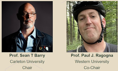
- Prof. Sean Barry, Carleton University

- Prof. Paul Ragogna, Western University


Scientific Committee:

- Adrie Mackus, Eindhoven University of Technology

- Anjana Devi, Ruhr University Bochum

- Annelies Delabie, IMEC

- Anuja DaSilva, Lam Research

- Dennis Hausmann, Lam Research

- Erwin Kessels, Eindhoven University of Technology

- Gregory Parsons, North Carolina State University

- Han-Bo-Ram Lee, Incheon National University

- Ishwar Singh, IBM

- Keyvan Kashefi, Applied Materials

- Kristen Colwell, Intel

- Mark Saly, Applied Materials

- Marko Tuominen, ASM

- Ralf Tonner-Zech, Wilhelm-Ostwald-Institute für Physikalische und Theoretische Chemie

- Ravi Kanjolia, EMD Electronics

- Robert Clark, TEL

- Sang Hoon Ahn, Samsung Electronics

- Seung Wook Ryu, SK hynix

- Stacey F. Bent, Stanford University

Contact Information:

asd2024.ca

Monday, June 19, 2023

Revolutionary Study Unveils Enhanced Uniformity and Selectivity in TiO2 Films for Nanoelectronics Manufacturing

Researchers Achieve 2× Improvement in TiO2 Film Thickness and Pattern-dependent Uniformity in 45 nm Half-pitch Patterns

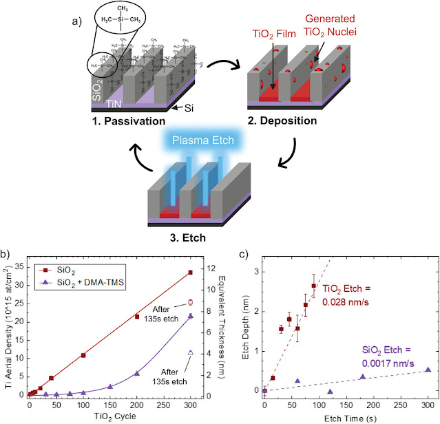
In a groundbreaking study, researchers have made significant advancements in the area-selective deposition (ASD) of TiO2 films, bringing unprecedented uniformity and selectivity to nanoelectronics manufacturing. The research, led by Rachel A. Nye and her team at imec, KU Leuven, and North Carolina University, demonstrates the successful implementation of passivation + deposition + etch supercycle process in industrially relevant 45 nm half-pitch patterns.


By leveraging the unique capabilities of the DMA-TMS inhibitor, the researchers achieved remarkable results. The TiO2 atomic layer deposition (ALD) process yielded a 2× improvement in film thickness, depositing approximately 8 nm of TiO2 with 88% uniformity and 100% selectivity on SiO2/TiN line/space patterns. Moreover, the study revealed lower defectivity on pattern sidewalls, top surfaces, and corners compared to previous reports.

A key finding was pattern-dependent uniformity, emphasizing the significance of understanding and optimizing processes at specific feature scales. As feature sizes continue to shrink, the researchers anticipate further improvements in uniformity. The study also highlighted the importance of refining passivation, deposition, and etch parameters for enhanced selectivity and uniformity control.

The research opens doors to a wide range of applications for TiO2 thin films in nanoelectronics, including antireflection coatings, sensors, photocatalysts, and etch-resistant layers. The study provides valuable insights into the quantification of uniformity and selectivity in nanoscale patterns, serving as a benchmark for future advancements in nanoscale ASD. The results have significant implications for the design and fabrication of electronic devices on an industrial scale.

Monday, September 26, 2022

Meet Atlant3D Technologies with CEO Maksym Plakhotnyuk


ATLANT 3D Nanosystem is part of the SSAP Europe portfolio and is a global pioneer combining unique advanced technologies to enable atomic layer 3D printing. Listen to their CEO & Founder Maksym Plakhotnyuk as he gives us the rundown on his cutting-edge technology that has the potential to change the world in big ways. 🌎 Learn more: https://www.atlant3d.com/

Thursday, September 1, 2022

UPDATE - ASD 2023 will be held in Incheon National University South Korea April 2-5, 2023

ASD2023 will be held in Incheon National University from April 2nd to 5th, 2023. An official website will be online soon! Stay tuned!

Included is a session on ALD for Semiconductor applications.

UPDATE - website is online: http://asd2023.com


PROGRAM COMMITTEE:
  • Rudy J Wojtecki (IBM)
  • Stacey F Bent (Stanford University)
  • Annelies Delabie (imec)
  • John G Ekerdt (University of Texase)
  • Dennis Hausmann (Lam Research)
  • Erwin Kessels (Eindhoven University of Technology)
  • Adrie Mackus (Eindhoven University of Technology)
  • Ravi Kanjolia (EMD Electronics)
  • Gregory Parsons (North Carolina State University)
  • Robert Clark (TEL)
  • Sean Barry (Carleton University)
  • Han-Bo-Ram Lee (Incheon National University)
  • Marko Tuominen (ASM)
  • Sudipto Naskar (Intel)
  • Anuja DaSilva (Lam Research)
  • Kristen Colwell (Intel)

Wednesday, June 22, 2022

NCD supplied ALE and ASD equipment to Samsung Electronics Co., Ltd.

NCD has recently supplied ASD (Area Selective Deposition) equipment to Samsung Electronics Co., Ltd. Following ALE (Atomic Layer Etching).

This is the cluster system which consists of two process modules (PMs) and a wafer transfer module (TM) and applies a running program for process integration. In addition, it is equipped to process at high temperatures up to 500℃ and process with ozone and plasma for developing the next semiconductor devices.

ALE is able to etch a deposited layer by atomic scale as opposed to ALD and ASD can only deposit on the selective area not grow the whole area of substrates by ALD.

Today, lots of universities, institutes, and companies have actively been developing future high-tech and highly integrated devices using ALE and ASD processes.

NCD expects that the ALE/ASD system will contribute very much to the development of high-end semiconductor technology and is going to do all of the efforts to the best ALD equipment company with new challenges and continuous R&D.

<Lucida M200PL Series ALD System>


Friday, January 7, 2022

TSMC Self-Aligned Via Process Development for Beyond the 3nm Node

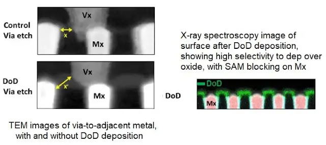
Semiwiki Tom Dillinger reports on an interesting paper by TSMC at the recent IEDM 2021 conference in San Francisco using selective ALD with the help of SAMs or Dielectric on Dielectric (DOD) as it is called.


From the article sumary: Continued interconnect scaling below the 3nm node will necessitate unique process development research to maintain electrical and reliability specs in the presence of (up to 4nm) overlay error. The need for low-K interlevel dielectrics is a given – yet, the via etch in these materials is not especially tolerant of EPE.

TSMC has demonstrated a potential process flow for a “self-aligned via” with an additional DoD material. The etch rate differential of the DoD results in more robust via-to-adjacent metal reliability. This process flow utilizes two unique steps – the SAM of a blocking material on metal surfaces, and the selective ALD of a dielectric-on-dielectric.

Tuesday, December 14, 2021

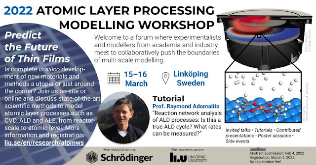
2022 Atomic Layer Processing Modelling Workshop

Pedersen group is organizing a work shop on modelling of atomic layer processes in Linköping 15-16 March next year with a Tutorial by Ray Adomaitis. Possibility to join via Zoom. 


Welcome to a forum where experimentalists and modellers from academia and industry meet to collaboratively push the boundaries of multi-scale modelling.

Predict the Future of Thin Films

Is complete in silico development of new materials and methods a utopia or just around the corner? Join us on-site or online and discuss state-of-the-art scientific methods to model atomic layer processes such as CVD, ALD and ALE, from reactorscale to atomic level.

The conference will have a mix of contributed talks, describing the latest in ALP modelling (atomic layer processing) and industry lectures presenting areas that need modelling. 

Tutorial

Prof. Raymond Adomaitis, from University of Maryland, will describe his way of modelling ALP in the tutorial “Reaction network analysis of ALD processes: Is this a true ALD cycle? What rates can be measured?”.


Date and time: March 15-16, starting on Tuesday at 12.00. 

Place: Planck, Fysikhuset. You will also be able to participate online via link.

Abstract deadline: February 2022.

The conference is free of charge but to participate you will have to register. Registration and Abstract aplication will soon be available here.


Tuesday, October 5, 2021

Call for Abstracts - 6th Area Selective Deposition Workshop (ASD 2022)


Call for Abstracts, Due February 7, 2022

An effort to help facilitate the progression of ASD techniques, the 6th Area Selective Deposition Workshop (ASD 2022) scheduled for April 21-22, 2022, in San Francisco will act as a central event for sharing and discussing the newest developments in ASD by gathering leading experts from both academia and industry. Attendees can expect to participate in talks regarding fundamental challenges related to recent developments in ASD, applications for ASD in next-generation technology, emergent processes for implementing ASD techniques, and new perspectives on metrological and characterization strategies for further understanding persistent mechanistic challenges. Based on the success of the previous workshops, ASD 2022 will consist of two days of presentations by invited and contributing speakers, as well as a banquet reception and poster session.

Topics:

This event is centered on showcasing developments across the whole spectrum of area-selective deposition. Thus, the Workshop will cover a wide range of topics including the following:

· Near Term Technology Readiness (Scalable and Relevant ASD Processes for Use in Manufacturing)
· Fundamentals of ASD (Defects, Growth Mechanisms and Inhibitor Chemistries)
· Metrology Techniques for ASD
· Emerging/Exploratory ASD Processes and Applications (e.g., Catalysis, Energy Generation and Storage)


Key Deadlines:

Call for Abstracts Deadline: February 7, 2022
Author Acceptance Notifications: February 21, 2022
Hotel Reservation Deadline: March 4, 2022
Early Registration Deadline: March 4, 2022


Program Chair:

Rudy J. Wojtecki
IBM Almaden Research Center, USA
Questions? Contact rjwojtec@us.ibm.com


Thursday, September 30, 2021

Selectivity Enhancement for Ruthenium Atomic Layer Deposition in Sub-50 nm Nanopatterns by Diffusion and Size-Dependent Reactivity

Area-selective deposition (ASD) is a promising bottom-up approach for fabricating nanoelectronic devices. The challenge is to prevent the undesired growth of nanoparticles in the nongrowth area. 

In this work from Belgium and The Netherlands research teams, linewidths of 50 nm and smaller, all Ru adspecies are captured at the growth interface before growth by precursor adsorption is catalyzed. This is more than 1000 times lower than for patterns with a linewidth of 200 nm and larger, where the Ru content decreases significantly only near the interface with the growth surface. 

The predicted depletion zone is confirmed by experiments in nanoscale line-space patterns. Overall, this mechanism results in smaller and fewer Ru nanoparticles for smaller patterns, facilitating the development of passivation-deposition-etch ASD processes for nanoelectronic device fabrication.

Selectivity Enhancement for Ruthenium Atomic Layer Deposition in Sub-50 nm Nanopatterns by Diffusion and Size-Dependent Reactivity

Jan-Willem J. Clerix, Esteban A. Marques, Job Soethoudt, Fabio Grillo, Geoffrey Pourtois, J. Ruud Van Ommen, Annelies Delabie,
3 September 2021


Area-selective deposition (ASD) is a promising bottom-up approach for fabricating nanoelectronic devices. However, a challenge is to prevent the undesired growth of nanoparticles in the nongrowth area. This work uses kinetic Monte Carlo (KMC) methods to investigate the defectivity in ruthenium ASD by (ethylbenzyl)(1-ethyl-1,4-cyclohexadienyl)Ru/O2 (EBECHRu) atomic layer deposition (ALD) in line-space nanopatterns with different dimensions. Ru ASD is governed by adsorption as well as diffusion. The defectivity depends on the pattern dimensions, as nanoparticles can diffuse and reach the interface with the growth area where they aggregate. For linewidths of 50 nm and smaller, all Ru adspecies are captured at the growth interface before growth by precursor adsorption is catalyzed. The synergetic effect of diffusion and size-dependent reactivity reduces defectivity below 1010 Ru atoms cm−2 for at least 1000 ALD cycles. This is more than 1000 times lower than for patterns with a linewidth of 200 nm and larger, where the Ru content decreases significantly only near the interface with the growth surface. The predicted depletion zone is confirmed by experiments in nanoscale line-space patterns. Overall, this mechanism results in smaller and fewer Ru nanoparticles for smaller patterns, facilitating the development of passivation-deposition-etch ASD processes for nanoelectronic device fabrication.


Saturday, September 18, 2021

University of Helsinki presents Self-Aligned Thin-Film Patterning by Area-Selective Etching of Polymers

A promising path to cut cost, scale, and reduce the environmental impact of semiconductor manufacturing

One of the driving costs in the high volume production of semiconductor components for especially powerful processors and memory chips is the patterning process. Both the capital investment in photolithographic equipment and the design cost add to the escalating cost going down to smaller nodes (see figure below). If one can reduce the number of lithographic mask layers needed in the production for a chip design one automatically cut the overall cost. Another problem is that while scaling down designs to smaller critical dimensions and tighter pitches and scaling up in the 3rd dimension like for 3D-NAND and coming 3D-DRAM it becomes more difficult to match the next mask layer with the previous one. The industry has solved this issue successfully for many years by introducing self-aligned processes like self-aligned contacts to the source, drain, and gate of the transistors below. Also, selective deposition processes like selective Epi and Cobalt CVD caps on copper are in production.

From an environmental view, lithography and mask more mask layers also consume more energy and clean water. Recent reports from Taiwan have it that both are problems, where drought has led to water shortages and the overall energy demand from fabs are high (about 5% of Taiwan total demand in 2019). 

Here, the University of Helsinki presents a process sequence for the future that is self-aligned and selective making it possible to mitigate all those problems in a very clever way for future devices and metallization schemes - please find all the details in the article below that is open source for download.

Self-Aligned Thin-Film Patterning by Area-Selective Etching of Polymers

by Chao Zhang, Markku Leskelä and Mikko Ritala *

Coatings 2021, 11(9), 1124; https://doi.org/10.3390/coatings11091124

Patterning of thin films with lithography techniques for making semiconductor devices has been facing increasing difficulties with feature sizes shrinking to the sub-10 nm range, and alternatives have been actively sought from area-selective thin film deposition processes. Here, an entirely new method is introduced to self-aligned thin-film patterning: area-selective gas-phase etching of polymers. The etching reactions are selective to the materials underneath the polymers. Either O2 or H2 can be used as an etchant gas. After diffusing through the polymer film to the catalytic surfaces, the etchant gas molecules are dissociated into their respective atoms, which then readily react with the polymer, etching it away. On noncatalytic surfaces, the polymer film remains. For example, polyimide and poly(methyl methacrylate) (PMMA) were selectively oxidatively removed at 300 °C from Pt and Ru, while on SiO2 they stayed. CeO2 also showed a clear catalytic effect for the oxidative removal of PMMA. In H2, the most active surfaces catalysing the hydrogenolysis of PMMA were Cu and Ti. The area-selective etching of polyimide from Pt was followed by area-selective atomic layer deposition of iridium using the patterned polymer as a growth-inhibiting layer on SiO2, eventually resulting in dual side-by-side self-aligned formation of metal-on-metal and insulator (polymer)-on-insulator. This demonstrates that when innovatively combined with area-selective thin film deposition and, for example, lift-off patterning processes, self-aligned etching processes will open entirely new possibilities for the fabrication of the most advanced and challenging semiconductor devices.


Schematics showing self-aligned polymer etching and the subsequent film patterning through area-selective deposition and lift-off processes. (Zhang et al Coatings 2021, 11(9), 1124, figure 1)

This is an open access article distributed under the Creative Commons Attribution License which permits unrestricted use, distribution, and reproduction in any medium, provided the original work is properly cited

Semiconductor design and manufacturing: Achieving leading-edge capabilities, McKinsey LINK

Monday, April 5, 2021

Intermolecular at the AVS ASD2021 Workshop, April 6-8.

Join Milind Weling as he talks with fellow panelists Robert D. Clark (TEL) Annelies Delabie (imec), Adrie Mackus (Eindhoven University of Technology) Anuja De Silva (Lam) on Area Selective Deposition at ASD2021 on April 8 at 12:50PM CDT, 10:50 AM Pacific. Moderated by Rudy Wojtecki (IBM).


Join EMD Electronics and program co-chairs John Ekerdt & Stacey Bent at the Area Selective Deposition Workshop, April 6-8.

Day 1: April 6
Poster Session at 2 pm • Lanxia Cheng presents “Area Selective Deposition of Electronics using Multilayer SAM as Surface Passivation.”

Day 2: April 7
Session 4 is chaired by Ravindra Kanjolia., EMD Electronics

Poster Session at 2 pm • Lanxia Cheng presents “Area Selective Deposition of Electronics using Multilayer SAM as Surface Passivation.”

Day 3: April 8
Session 8 at 11:30 am • Ravindra Kanjolia presents, EMD Electronics “Strategies for Area Selective Deposition: From Inherently Selective Precursors to Inhibitor Molecules and Processes.”

12:50 pm • Milind Weling participates on a panel discussion “Area Selective Deposition.”

Tuesday, March 9, 2021

April 6-8 5th Area Selective Deposition Workshop (ASD 2021)

In an effort to help facilitate the progression of ASD techniques, The University of Texas at Austin University is proud to host the 5th Area Selective Deposition Workshop (ASD 2021), which will be held on April 6-8, 2021. The Area Selective Deposition Workshop scheduled for April 2-3 (ASD 2020) was postponed in March 2020 due to public health concerns relating to the coronavirus disease (COVID-19) and was later canceled in anticipation of ASD 2021. ASD 2021 retains much of the character of previous workshops and what was intended for ASD 2020, albeit in a virtual format. This year’s workshop will act as a central event for sharing and discussing the newest developments in ASD by gathering leading experts from both academia and industry. Attendees can expect to participate in talks regarding fundamental challenges related to recent developments in ASD, applications for ASD in next-generation technology, emergent processes for implementing ASD techniques, and new perspectives on metrological and characterization strategies for further understanding persistent mechanistic challenges.
Key Deadlines:
Early Registration Deadline: March 16, 2021
Questions? Contact ekerdt@utexas.edu


The workshop will begin at 10:00 am (CST) and end at 3:00 pm on April 6 and 7 and at 2:00 pm on April 8. Times have been selected to enable participation for registrants spanning the West Coast to Europe. The workshop will include live sessions consisting of invited and contributed talks and panel discussions. A session moderator will ask questions that are entered onto the meeting presentation platform from registrants. Live poster sessions will be held after the oral presentation sessions on April 6 and 7; poster presenters will preload five-minute oral highlights of their poster one week before the workshop.

Invited speakers:
    • Chris Bates, UC Santa Barbara, USA
    • Fabio Grillo, ETH Zurich, Switzerland
    • Ravi Kanjolia, EMD Electronics, USA
    • Shashank Misra, Sandia National Labs, USA
    • Ainhoa Romo Negreira, TEL, Belgium
    • Tania Sandoval, Universidad Técnica, Chile
    • Kavita Shah, Nova, USA
    • Amy Walker, UT Dallas, USA
    • Charles Wallace, Intel, USA

Wednesday, February 3, 2021

Call for Abstracts - The 5th AVS Area Selective Deposition Workshop (ASD 2021)

Developments in nanoelectronics and nanoscale surface modification have continued to drive the need for more elegant and reliable bottom-up area selective deposition (ASD) strategies. Most notably, the semiconductor industry has relentlessly pursued sub-10 nm transistor fabrication for next-generation devices, an endeavor that increasingly relies on selective deposition techniques to facilitate proper material alignment. However, other fields beyond traditional transistor fabrication have also found potential applications for selective deposition. Mixed-material catalysts have consistently shown the benefits of having site-specific material growth, but new optical devices and materials for energy storage have also contributed to an increased focus on developing new strategies for ASD.


In an effort to help facilitate the progression of ASD techniques, The University of Texas at Austin University is proud to host the 5th Area Selective Deposition Workshop (ASD 2021), which will be held on April 6-8, 2021. The Area Selective Deposition Workshop scheduled for April 2-3 (ASD 2020) was postponed in March 2020 due to public health concerns relating to the coronavirus disease (COVID-19) and was later cancelled in anticipation of ASD 2021. ASD 2021 retains much of the character of previous workshops and what was intended for ASD 2020, albeit in a virtual format. This year’s workshop will act as a central event for sharing and discussing the newest developments in ASD by gathering leading experts from both academia and industry. Attendees can expect to participate in talks regarding fundamental challenges related to recent developments in ASD, applications for ASD in next-generation technology, emergent processes for implementing ASD techniques, and new perspectives on metrological and characterization strategies for further understanding persistent mechanistic challenges.

Wednesday, August 5, 2020

Applied Materials launch Selective Tungsten CVD for their Endura(TM) platform

[Applied Materials Blog LINK] Tungsten has been widely used as a gapfill material in middle-of-line (MOL) contacts for its low resistivity and bulk fill characteristics. MOL contacts form the critical electrical link between the transistors and the interconnects. Hence, ensuring low resistivity contacts is crucial for overall device performance.

With continued scaling, however, contact dimensions have decreased to the point at which contact resistance is becoming a bottleneck in realizing optimum device performance. As the cross-sectional area of the contact shrinks, a growing proportion of the volume is occupied by metal liner/barrier and nucleation layers, leaving less volume for the conducting metal fill. In addition, multiple resistive interfaces in the plug contribute to higher contact resistance.

An Applied Materials Endura(TM) Platform equipped with seven Selective Tungsten CVD Volta(R) and 2 pre-clean 300 mm chambers. (Credit: Applied Materials)

The Applied Endura Volta Selective W CVD system offers an integrated materials solution that relieves these adverse effects with a breakthrough in 2D scaling. The system combines surface treatment chambers with selective tungsten deposition chambers. The selective deposition is enabled by both the unique process capabilities of the deposition chambers and the various surface treatments that use specialized chemistries to prepare the underlying metal and dielectrics of the contact to enable bottom-up, metal-on-metal deposition. The selective process eliminates both liner/barrier and nucleation layers to alleviate the bottleneck in device performance, and produces void- and seam-free gapfill.

Cross section of a leading edge Logic processor showing the Source/Drain contacts to the transistors and the metal interconnetcs (Credit: TechInsight, Applied Materials)

As all process steps are performed in an ultra-clean, continuous high-vacuum environment, the integrated materials solution ensures a pristine interface and defect-free contact fill. With the volume of conducting metal maximized, contact resistivity is substantially improved compared to conventional liner/barrier contact fabrication. This lower resistance facilitates higher device density and extends 2D scaling.

The selctive W CVD defect-free contact fill maximizes the volume of conducting metal (right), contact resistivity is substantially improved compared to conventional liner/barrier contact fabrication (left). (Credit: Applied Materials)

Friday, February 7, 2020

AVS ASD20 - Call for Abstracts MONDAY February 10, 2020

In an effort to help facilitate the progression of ASD techniques, the 5th Area Selective Deposition Workshop (ASD 2020) will act as a central event for sharing and discussing the newest developments in ASD by gathering leading experts from both academia and industry Attendees can expect to participate in talks regarding fundamental challenges related to recent developments in ASD, applications for ASD in next-generation technology, emergent processes for implementing ASD techniques, and new perspectives on metrological and characterization strategies for further understanding persistent mechanistic challenges. Based on the success of the previous workshops, ASD 2020 will consist of two days of presentations by invited and contributing speakers, as well as a banquet reception and poster session.


Abstract Deadline: February 10, 2020 LINK
 

Monday, January 6, 2020

Introductory and advanced courses on ALD and ALE in Eindhoven

Reminder - ALD Academy event coming up next week (January 14/15) in Eindhoven: Introductory and advanced courses on ALD and ALE - there is still room for a some last-minute registrations. Lecturers are Adrie Mackus, Harm Knoops, Gregory Parsons and Erwin Kessels.
 
 
  • Introductory ALD course: A concise course in which the method of atomic layer deposition (ALD) will be introduced and in which several key aspects of ALD will be addressed. This course is intended for newcomers in the field of ALD or for those that want to brush up their knowledge of ALD. This part of the course will be given by Erwin Kessels and Greg Parsons.
  • Advanced ALD course: This is an interactive course on ALD in which more advanced aspects of ALD will be discussed. Especially conceptual and practical aspects will be addressed which one encounters when exploring new ALD processes, materials and applications. This course is intended for those having experience in ALD but who would like to learn more about additional possibilities and opportunities that ALD can provide. This part of the course will be given by Adrie Mackus, Harm Knoops, Greg Parsons and Erwin Kessels.
  • ALE course: This is a new course that starts at the introductory level presenting the method of atomic layer etching (ALE) and then go to a more advanced level. It will describe several ALE approaches and review the ALE processes developed. Also the state-of-the-art of the technology will be presented in terms of practical aspects for those interested in the method. This part of the course will be given by Erwin Kessels, Harm Knoops, Adrie Mackus, and Greg Parsons.
 Event page: LINK


Thursday, September 12, 2019

The website for the 2020 Area Selective Deposition Workshop is now live!

Developments in nanoelectronics and nanoscale surface modification have continued to drive the need for more elegant and reliable bottom-up area selective deposition (ASD) strategies. Most notably, the semiconductor industry has relentlessly pursued sub-10 nm transistor fabrication for next-generation devices, an endeavor that increasingly relies on selective deposition techniques to facilitate proper material alignment. However, other fields beyond traditional transistor fabrication have also found potential applications for selective deposition. Mixed-material catalysts have consistently shown the benefits of having site-specific material growth, but new optical devices and materials for energy storage have also contributed to an increased focus on developing new strategies for ASD.


In an effort to help facilitate the progression of ASD techniques, Stanford University is proud to host the 5th Area Selective Deposition Workshop (ASD 2020), held on April 2–3, 2020 in Palo Alto, California USA. Located in the heart of Silicon Valley, this year’s workshop will act as a central event for sharing and discussing the newest developments in ASD by gathering leading experts from both academia and industry. Attendees can expect to participate in talks regarding fundamental challenges related to recent developments in ASD, applications for ASD in next-generation technology, emergent processes for implementing ASD techniques, and new perspectives on metrological and characterization strategies for further understanding persistent mechanistic challenges.

Based on the success of the previous workshops, ASD 2020 will consist of two days of presentations by invited and contributing speakers, as well as a banquet reception and poster session at Stanford University. We hope that guests will also have time to experience some of the local attractions and natural beauty that the Bay Area has to offer!

Sunday, July 7, 2019

Rapid and Selective Deposition of Patterned Thin Films on Heterogeneous Substrates via Spin Coating

[Tokyo Electron] Researchers at UC Santa Barbara along with TEL and SRC have collaborated to develop new methods for selective spin coating. With wide-ranging applications in the future of semiconductor patterning as device makers are challenged to build more complex transistors and simultaneously lower costs. 

They demonstrate that accurate control over the process parameters allows incomplete trichlorosilane self-assembled monolayers (SAMs) to induce spin dewetting on both homogeneous (SiO2) and heterogeneous (Cu/SiO2 or TiN/SiO2) surfaces. Under optimal conditions, spin dewetting on line–space patterns results in the selective deposition of polymer over regions not functionalized with SAM.  

Source: "Rapid and Selective Deposition of Patterned Thin Films on Heterogeneous Substrates via Spin CoatingLINK

Monday, June 3, 2019

VLSI 2019 Workshop - The Impact of Atomic Layer Processing and Selective Area Patterning on Device Fabrication and Performance

On June 9th, the 2019 Symposia on VLSI Technology and Circuits will feature a free workshop on The Impact of Atomic Layer Processing and Selective Area Patterning on Device Fabrication and Performance. This workshop is endorsed by the AVS and features presentations from some prominent members of the AVS community. If you happen to be attending the VLSI Symposia, or have colleagues who are planning to attend, please let them know about this opportunity hear about the impact of ALD/ALE on device properties and to further develop the link between the ALD/ALE process community and the semiconductor device and circuits community. 


Any additional questions you may have, please feel free to reach out to Eric Joseph, the workshop organizer, to the workshop committee (which consists of the 2019 ALD Conference / ALE Workshop Chairs) or to the VLSI or AVS staff. 
 
More information: LINK
 

Tuesday, April 2, 2019

RASIRC to Highlight Precise Water Vapor Delivery in Area Selective Deposition

CTO featured as industry expert on panel at upcoming ASD Workshop

San Diego, Calif – March 29, 2019 – RASIRC will discuss test results for precise delivery of water vapor at the Area Selective Deposition (ASD) 2019 Workshop on April 4-5 in Leuven, Belgium. The company, a Silver Sponsor of the workshop, will review droplet and particle measurements as well as mass delivery under a variety of conditions. The RASIRC poster entitled “Precise Control of Water Vapor Delivery for ASD” will be displayed on Thursday April 4 and Friday April 5 as part of the workshop’s poster session. Additionally, RASIRC CTO Daniel Alvarez will be a speaking on the “Critical Challenges and Research Needs for ASD” panel during the 4th ASD workshop. The panel discussion will take place on Friday April 5 from 15:00 to 16:00.

“In order for the industry to take this to a high volume commercial level, we first must have an understanding of the underlying chemical pathways associated with ASD,” says Alvarez. “It is critical to control nucleation, which is best accomplished by the control of adsorption and surface properties on an atomic level.”
 
 
ASD Workshop is an annual event sponsored by ASM and IMEC. The workshop features leading academic and industry experts in surface chemistry, new processes, metrology, fields of applications and all technology needs and challenges for ASD.

“Controlled water addition at low concentration and temperature is vital to successful selectivity in ASD processes,” said Jeffrey Spiegelman, RASIRC President and Founder. “That is why we designed a water ampoule replacement that utilizes a membrane delivery system for precise delivery of droplet-free water vapor. Our data shows that we can achieve the required mass output in a repeatable and consistent manner.”

Spiegelman and Alvarez will be available to discuss the company’s ASD product line-up, which includes hydrogen peroxide and hydrazine gas delivery in addition to water vapor.

About RASIRC Products

RASIRC RHA enables the delivery of purified water vapor into low pressure processes. The membrane delivery system separates the liquid water and its headspace from directly seeing the process vacuum. The membrane assembly allows the mass transfer of water vapor at a known diffusion rate for a given set of parameters (temperature, pressure, surface area, carrier gas flow rate).

BRUTE® Peroxide is a novel oxidant that improves nucleation density at film interfaces when compared to other oxidants. Surface functionalization is more dense and initiation is faster using anhydrous hydrogen peroxide gas compared with alternatives. This can allow for better selectivity and less damage to metal surfaces in ASD processes.

BRUTE® Hydrazine enables uniform nitride deposition for Silicon and early transition metals at low temperature. BRUTE® Hydrazine may also be used as an atomic hydrogen source, where metals such as Ru, Cu, and Co may be cleaned and reduced. Hydrazine gas is generated in situ and is virtually water free. Brute Hydrazine has been formulated for a relatively high flash point for safer handling.

RASIRC Peroxidizer® provides high volumes of reactive H2O2/H2O mixtures for high throughput ALD. This reactive gas generator is ideal for roll-to-roll ALD coatings that require high speed deposition at reduced temperatures.

Additional RASIRC products include the RainMaker Humidification System (RHS) and the Hydrogen Peroxide Steamer (HPS). The RHS generates water vapor for oxidation applications and the HPS provides surface cleaning, preconditioning, wet thermal oxidation and residual carbon removal.