Saturday, June 13, 2015

Simulation of a Multihole outlet Savannah ALD reactor

For those of you interested in ALD reactor simulations and especially the classic cross flow design you should definitely check out this publication. University of Wisconsin-Milwaukee, University of Alaska Anchorage and Macquarie University, Sydney.

Investigating atomic layer deposition characteristics in multi-outlet viscous flow reactors through reactor scale simulations

Mohammad Reza Shaeri,Tien-Chien Jen, Chris Yingchun Yuan, Masud Behnia
Available online 6 June 2015


The Atomic Layer Deposition system at the Laboratory for Sustainable and Nano-Manufacturing in Milwaukee was required in October 2009 from Cambridge Nanotech Inc. (Today Ultratech / Cambrideg Nanotech). The Model is a Savannah S100 with capabilities for 100 mm wafers up to 10 wafer batch processing in a single deposition (https://pantherfile.uwm.edu/cyuan/Facilities.html). Either this is actually a picture from 2009 when the tool was new or these guys take really good care of their equipment as indicated that the protective shipping foil is still on.


Abstract
In order to minimize the operational time of atomic layer deposition (ALD) process, flow transports and film depositions are investigated in multi-outlet viscous flow reactors through reactor scale simulations. The simulation process is performed on depositions of Al2O3 films using trimethylaluminum and ozone as the precursors, and inert argon as the purge gas. The chemistry mechanism used includes both gas-phase and surface reactions. Simulations are performed at a fixed operating pressure of 10 Torr (1330 Pa) and at two substrate temperatures of 250 °C and 300 °C, respectively. Flows inside the reactors are following the continuum approach; as a result, the Navier–Stokes, energy and species transport equations can be used to simulate transient, laminar and multi-component reacting flows. Based on the chemistry mechanism adopted in this study, the amount of oxygen atoms produced from the ozone decomposition is found to be the major reason for discrepancies in oxidation times and deposition rates at different ALD processes. A reactor with fewer outlets minimizes the ALD operational times by reducing both oxidation time and second purge time. In addition, higher deposition rates at a shorter time are obtained by using a reactor with fewer outlets. However, assigning a long enough time for the ozone exposure results in independency of ALD characteristics from the number of outlets such that the growth rates of around 3.78 angstrom/cycle and 4.52 angstrom/cycle are obtained for the substrate temperatures of and , respectively.

At Lund Nano Lab in Sweden we also operate a Savannah from about the same time and it is one of the more popular tools judging by the frequent user bookings. Since Ultratech came in the picture some things have happened. Today you get a slim white design Generation 2 and the delivery time in Europe can be as fast as 8 weeks which is pretty fast if you ask me. Check out the new product page at Cambridge Nanotech here.


The Savannah is available in three configurations: S100, S200, and S300 and is capable of holding substrates of different sizes (up to 300mm for the S300). 


Friday, June 12, 2015

Samsung and SNU identifies the next Super High-k

Here is another publication from Samsung on high-k screening in collaboration with Academia. This time in collaboration with researchers from the home base at Seoul National University. This is somehow a new behavior of Samsung who actually withdrew talks in front of ALD 2012 in Dresden on anything realting to high-k and DRAM development and I have not seen that much publishing from Samsung since then on these topics. Calculated results do usually not tend to interest me but this one is very, very interesting and I think it will take me some time to go there it - fully understand I will not.


"Except for c-BeO, we could not find any outstanding high-κ dielectrics with eitherEg or κ larger than those of the HfO2 thin films currently used in CPU or DRAM (Eg~6.0 eV and κ~20–25; see t-HfO2)"


Cubic BeO will probably be a hot ALD topic for the rest of 2015 and I do wonder if Prof. Wang will mention BeO in Portland at the AVS ALD 2015 in Portland when he gives his invited talk: 

Cheol Seong Hwang, Seoul National University
“Capacitor Dielectric and Electrodes for DRAM with sub-20 nm Design Rule”

Check out the paper - it is Open Access - thank you Samsung!

Novel high-κ dielectrics for next-generation electronic devices screened by automated ab initio calculations (Open Access)

Kanghoon Yim, Youn Yong, Joohee Lee, Kyuhyun Lee, Ho-Hyun Nahm, Jiho Yoo, Chanhee Lee, Cheol Seong Hwang and Seungwu Han

NPG Asia Materials (2015) 7, e190; doi:10.1038/am.2015.57
Published online 12 June 2015


The experimental band gap and dielectric constant for well-known oxides. The property region ideal for dielectrics is also shown.


Abstract:
As the scale of transistors and capacitors in electronics is reduced to less than a few nanometers, leakage currents pose a serious problem to the device’s reliability. To overcome this dilemma, high-κ materials that exhibit a larger permittivity and band gap are introduced as gate dielectrics to enhance both the capacitance and block leakage simultaneously. Currently, HfO2 is widely used as a high-κ dielectric; however, a higher-κ material remains desired for further enhancement. To find new high-κ materials, we conduct a high-throughput ab initiocalculation for band gap and permittivity. The accurate and efficient calculation is enabled by newly developed automation codes that fully automate a series of delicate methods in a highly optimized manner. We can, thus, calculate >1800 structures of binary and ternary oxides from the Inorganic Crystal Structure Database and obtain a total property map. We confirm that the inverse correlation relationship between the band gap and permittivity is roughly valid for most oxides. However, new candidate materials exhibit interesting properties, such as large permittivity, despite their large band gaps. Analyzing these materials, we discuss the origin of large κ values and suggest design rules to find new high-κ materials that have not yet been discovered.


Eg vs κ plot for computed structures for 1158 oxides. Each point is color coded according to the figure of merit (Eg·κ). The candidate oxides that have not yet been tested are indicated by the chemical formula. The rough boundary of material properties that are adequate for each device type is marked by dashed lines. CPU, central processing unit.

Worth to mention also in this context is that Han Jin Lim from Samsung Semiconductor R&D Center will give a tutorial at the AVS ALD2015 conference at the end of June in Portland.

Han Jin Lim, Samsung Electronics, “ALD Technologies and Applications in Semiconductor Device Fabrication”


Abstract:
As semiconductor devices of both memory and logic have been smaller than 20nm feature size and beyond, it is most important to acquire the conformal high-quality thin films that effect on the electrical performance enhancement in the three dimensional patterned scheme. ALD technology has been required in such critical steps as transistor and capacitor and also increased its applications including DPT (double patterning technology).

This talk consists of two parts. The first part covers the ALD in general. Those introduce the general ALD technologies including processes, precursors, reactants and equipment. The second part deals with its applications in semiconductor device fabrication. Major applications include oxide for transistor gate and DPT pattrening, nitide for transistor spacer, high-k dielectrics for transistor as well as capacitor, and metal electrode.

Thursday, June 11, 2015

Samsung, NaMLab and KU Leuven present novel DRAM capacitor stack

There was a long time since I came across a publication on materials screening for the DRAM capacitor stack. That is why it is especially interesting to read of the joint work by NaMLab in Dresden , K.U. Leuven and Samsung. The team was able to enhance the properties of the high-k stack by replacing the Al2O3 interlayer with SrO to increase the overall k-value of the capacitor dielectric without degrading the barrier and leakage properties of the dielectric stack.


Introduction: For many years, the dynamic random access memory (DRAM) was the scaling driver in semiconductor industry. Continuous downscaling of the cell dimension led to the introduction of high-k materials in a three-dimensional cylindrical capacitor geometry with metal electrodes. Currently, the most common DRAM capacitor consists of a ZrO2/Al2O3/ZrO2 (ZAZ) stack. Intensive research is done on strontium titanate (STO) and Al doped TiO2 based capacitors, but here, the thickness scaling of the dielectric is difficult to reach due to the low band gap value of the TiO2 based dielectrics. Accordingly, additional research is necessary to scale the current ZrO2 based material stack.

Ultra-thin ZrO2/SrO/ZrO2 insulating stacks for future dynamic random access memory capacitor applications


Steve Knebel, Milan Pešić, Kyuho Cho, Jaewan Chang, Hanjin Lim, Nadiia Kolomiiets, Valeri V. Afanas'ev, Uwe Muehle, Uwe Schroeder and Thomas Mikolajick

J. Appl. Phys. 117, 224102 (2015); http://dx.doi.org/10.1063/1.4922349


(a) TEM micrograph of a ZAZ MIM film stack. The stack thickness is 10 nm. A distinct Al2O3 layer is visible in the center of the ZrO2 layer. ZrO2 grains stop growing at the Al2O3 interlayer. (b) TEM micrograph of a ZSrZ MIM film stack. Stack thickness is 5 nm. No distinct SrO layer is visible and the ZrO2 crystals are growing through the whole ZrO2 layer. (c) EDX line scan of the ZAZ film: a small Al peak can be seen in the center of the ZrO2 layer. (Inset) Zoom of the EDX line scan showing the Al peak and the background signal, which proves the position of the Al2O3 layer.
Citation: J. Appl. Phys. 117, 224102 (2015); http://dx.doi.org/10.1063/1.4922349


Aiming for improvement of the ZrO2-based insulator properties as compared to the state-of-the-art ZrO2/Al2O3/ZrO2 stacks beyond 20 nm dynamic random access memory (DRAM) technology applications, ultra-thin (5 nm) ZrO2/SrO/ZrO2 stacks with TiN electrodes deposited by physical vapor deposition are addressed. By replacing the Al2O3 interlayer with SrO, the effective dielectricpermittivity of the stack can be increased as indicated by electrical analysis. At the same time, no degradation of the insulating properties of the SrO-containing stacks and minor changes in the reliability, compared to an Al2O3 interlayer, are found. These results are indicating the possibility of further reducing the effective oxide thickness of the ZrO2-based stacks to come close to 0.5 nm for future DRAM capacitors.

International workshop ALD Russia 2015

International workshop Atomic Layer Deposition Russia 2015 (ALD Russia 2015)


Atomic Layer Deposition (ALD) is a thin film coating technique, which has gradually manifested itself as a powerful tool to fabricate ultrathin, highly uniform and conformal material layers for many applications including semiconductor integrated circuits industry, sensors, III-V devices, micro/nanoelectromechanical systems (MEMS/NEMS) manufacturing, optics, optoelectronics, solar cell production, biocompatible coatings for medical devices, etc. Although Russian (Soviet) scientists had played significant role in developing the scientific principles of the method in 1960s, until recently the potential of ALD technique for various applications was not fully exploited in Russia. Therefore the aim of the International Workshop ALD Russia 2015 is to consolidate the rapidly growing Russian ALD community, and to bring closer Russian researchers to the leading international experts in the field.


ALD Russia 2015 is organized by Moscow Institute of Physics and Technology.


The first announcement of ALD Russia 2015 can be downloaded here.

ALD Tutorial Speakers & Topics at AVS ALD 2015 in Portland

The tutorials for AVS ALD 2015 looks vey interesting indeed - word class ALD experts and speakers from Intel, University of Helsinki, SAFC, Samsung, IBM and Purdue University!

Tutorial Speakers & Topics 

The Tutorial will be held after noon on Sunday, June 28, 2015 at the Portland Hilton. The registration fee will include breaks and course materials.


Schedule


11:30 a.m.- 12:30 p.m.

Registration

12:30p.m.- 1:15 p.m.

Patricio E Romero, Intel, “Early stage ALD and CVD precursor development at Intel”

1:15 p.m.- 2:00 p.m.

Markku Leskelä, University of Helsinki, Finland, “ALD Process Development: Solutions to Industrial Challenges”

2:00 p.m.- 2:15 p.m.

Break

2:15 p.m.- 3:00 p.m.

Ravi Kanjolia, SAFC Hitech, "Lab to Fab: Precursor Development for Semiconductor Applications"

3:00 p.m.- 3:45 p.m.

HanJin Lim, Samsung Electronics, “ALD Technologies and Applications in Semiconductor Device Fabrication”

3:45 p.m.- 4:30 p.m.

Theodorus Standaert, IBM, “Challenges in BEOL Technology and Opportunities for ALD Processing"

4:30 p.m.- 4:45 p.m.

Break

4:45 p.m.- 5:30 p.m.
Peide D. Ye, Purdue University, “ALD for Novel Device Technologies”

Wednesday, June 10, 2015

Researchers at Rice University make ultrasensitive conductivity measurements

Here is a very interesting report that might indeed be interesting to characterize ALD growth in-situ ultra fast at optical frequencies!

(Nanowerk News) Researchers at Rice University have discovered a new way to make ultrasensitive conductivity measurements at optical frequencies on high-speed nanoscale electronic components.The research at Rice's Laboratory for Nanophotonics (LANP) is described online in a new study in the American Chemical Society's journal ACS Nano ("Charge Transfer Plasmons: Optical Frequency Conductances and Tunable Infrared Resonances"). In a series of experiments, LANP researchers linked pairs of puck-shaped metal nanodisks with metallic nanowires and showed how the flow of current at optical frequencies through the nanowires produced "charge transfer plasmons" with unique optical signatures.


Linked pairs of nanodisks as seen with a scanning electron microscope. (Image: Fangfang Wen/Rice University)


Tuesday, June 9, 2015

JVST A Special Issue on Atomic Layer Deposition 2016

As usual JVST A is Soliciting Research Articles for Publication in a Special January/February 2016 Issue on Atomic Layer Deposition.


This special issue is planned in collaboration with the 15th International Conference on Atomic Layer Deposition (ALD 2015) to be held in Portland, Oregon during June 28-July 1, 2015. The Special Issue will be dedicated to the science and technology of atomic layer controlled deposition of thin films. While a significant fraction of the articles are expected to be based on material presented at ALD 2015,research articles that are on ALD but were not presented at this conference are also welcome: the special issue will be open to all articles on the science and technology of ALD.

Manuscript Deadline: August 30, 2015 Click Here to Submit


Graphene-based sensor capable of detecting cholera toxins for diagnosis of cancer

As recently reported by The Silicon Republic, researchers have developed a graphene-based sensor that is capable of detecting cholera toxins and providing earlier diagnosis of cancer and other diseases.

The sensor, known as a Surface Plasmon Resonance (SPR) sensor, is an established optical technique for medical diagnosis with high sensitivity and specificity, and can potentially be used for lab-on-a-chip sensors.

‘This type of sensing platform offers a large variety for medical diagnostics, since it can be adapted to almost any type of disease markers’ — Prof Georg Duesberg, at the AMBER labs at Trinity’s School of Chemistry [One of the guys behind the Infineon /Qimonda carbon / high-k DRAM Trench Capacitor technology http://www.hes.ei.tum.de/fileadmin/w00bjl/www/uploads/Aichmayr_VLSI07_talk06.pdf]

Noncovalently Functionalized Monolayer Graphene for Sensitivity Enhancement of Surface Plasmon Resonance Immunosensors 

 Meenakshi Singh †‡, Michael Holzinger, Maryam Tabrizian, Sinéad Winters, Nina C. Berner, Serge Cosnier, and Georg S. Duesberg

J. Am. Chem. Soc., 2015, 137 (8), pp 2800–2803 DOI: 10.1021/ja511512m


Abstract

A highly efficient surface plasmon resonance (SPR) immunosensor is described using a functionalized single graphene layer on a thin gold film. The aim of this approach was two-fold: first, to amplify the SPR signal by growing graphene through chemical vapor deposition and, second, to control the immobilization of biotinylated cholera toxin antigen on copper coordinated nitrilotriacetic acid (NTA) using graphene as an ultrathin layer. The NTA groups were attached to graphene via pyrene derivatives implying π–π interactions. With this setup, an immunosensor for the specific antibody anticholera toxin with a detection limit of 4 pg mL–1 was obtained. In parallel, NTA polypyrrole films of different thicknesses were electrogenerated on the gold sensing platform where the optimal electropolymerization conditions were determined. For this optimized polypyrrole-NTA setup, the simple presence of a graphene layer between the gold and polymer film led to a significant increase of the SPR signal.

Monday, June 8, 2015

IBM Zurich present III-V on silicon wafers breakthrough technology using ALD

IBM has done it - a method of depositing ultra-fast III-V nanowires suitable for transistor channels and other structures on silicon-on-insulator (SOI) substrates -  and for sure ALD was involved in one of the early crucial processing steps to create the template for TASE - Template Assisted Selective Epitaxy. 

"A 30-nm-thick SiO2 layer covering the entire structure was conformally deposited using atomic layer deposition (ALD) " 

Check out the details below and in the Open Access paper!

Template-assisted selective epitaxy of III–V nanoscale devices for co-planar heterogeneous integration with Si (Open Access)

H. Schmid, M. Borg, K. Moselund, L. Gignac, C. M. Breslin, J. Bruley, D. Cutaia and H. Riel
Appl. Phys. Lett. 106, 233101 (2015); http://dx.doi.org/10.1063/1.4921962 


Schematic (a) and SEM images (b)–(d) illustrating stacking of Si and III-V NWs. (b) SEM image shows a tilted view of three stacked template structures. (c) SEM cross-section image of the Si NW stack and (d), TEM image of the GaAs NW stack (Appl. Phys. Lett. 106, 233101 (2015); http://dx.doi.org/10.1063/1.4921962)

III–V nanoscale devices were monolithically integrated on silicon-on-insulator (SOI) substrates by template-assisted selective epitaxy (TASE) using metal organic chemical vapor deposition. Single crystal III–V (InAs, InGaAs, GaAs) nanostructures, such as nanowires, nanostructures containing constrictions, and cross junctions, as well as 3D stacked nanowires were directly obtained by epitaxial filling of lithographically defined oxide templates. The benefit of TASE is exemplified by the straightforward fabrication of nanoscale Hall structures as well as multiple gate field effect transistors (MuG-FETs) grown co-planar to the SOI layer. Hall measurements on InAs nanowire cross junctions revealed an electron mobility of 5400 cm2/V s, while the alongside fabricated InAs MuG-FETs with ten 55 nm wide, 23 nm thick, and 390 nm long channels exhibit an on current of 660 μA/μm and a peak transconductance of 1.0 mS/μm at VDS = 0.5 V. These results demonstrate TASE as a promising fabrication approach for heterogeneous material integration on Si.


SEM images illustrating epitaxial filling of complex nano structures. (a) Evolution of the growth during filling of three templates, each having a lithographically pre-defined constriction. (b) Formation of an InAs cross-junction for the later fabrication of a Hall structure. The InAs film thickness is 23 nm (Appl. Phys. Lett. 106, 233101 (2015); http://dx.doi.org/10.1063/1.4921962).


The fabrication steps of TASE : a (100)-oriented SOI substrates (Soitec) with a device layer thickness of 25–50 nm were patterned using e-beam lithography and reactive ion etching. A 30-nm-thick SiO2 layer covering the entire structure was conformally deposited using atomic layer deposition (ALD) and annealed at 850 °C in Ar/H2. The SiO2 cap on one end of the Si structure was opened by patterning polymethylmethacrylate (PMMA) by e-beam lithography and buffered hydrofluoric acid (BHF) etching to expose the Si device layer. Next the Si was back-etched to the desired length using either XeF2 dry etching followed by tetramethylammoniumhydroxide (TMAH) wet etching or TMAH etching only, to result in well-defined {111} planes. The orientation of the {111} planes with respect to the channel direction was controlled by the alignment of the channel patterns. All structures reported here were patterned along the 〈110〉 direction. The as-prepared substrate was dipped in diluted (2.5%) HF to remove the native oxide on the exposed Si surfaces within the channels and was immediately loaded into the MOCVD reactor. Selective epitaxy of InGaAs was carried out using trimethylindium (TMIn), tertiarybutylarsine (TBAs), and trimethygallium (TMGa) at V/III ratio = 40 with TMIn/(TMIn+TMGa) = 0.5 at 580 °C. Chemical analysis was obtained from electron energy loss spectroscopy (EELS) analysis and indicated an In0.50Ga0.50As composition. InAs epitaxy was carried out at 520 °C using TMIn and TBAs with a V/III ratio = 80 and V/III ratio = 40 for the MuGFETs, respectively. Optionally, the dielectric template was removed after growth by wet etching in diluted HF, to expose the Si–III-V nano-structure on the SiO2 layer (BOX). 


Sunday, June 7, 2015

ALD and Beneq in the Innovation Hotspot for Nanomanufacturing

ALD is identified as one of the Paradigms of Innovation Hotspots in Nanomanufacturing in a recent Frost & Sullivan report on Innovations in Nanomanufacturing. Also a big congratulations to Beneq Oy from Finland, an ALD company identified as one of the "Key Stakeholders in Nanomanufacturing mastering". Beneq is mastering both ALD and Roll to Roll manufacturing.


New analysis from Frost & Sullivan, Innovations in Nanomanufacturing, finds that nanomanufacturing will gain traction in the next three to five years and is likely to approach commercialization between 2018 and 2020. Nanomanufacturing will find vast uses in consumer electronics, healthcare, automotive lighting, building automation, smart fabrics, display technology and positioning systems.


For complimentary access to more information on this research, please visit: http://bit.ly/1xL9GNe.

Current nanomanufacturing techniques do not support mass-scale production, as the fabrication of a large number of nano-devices repeatedly and under precisely controlled conditions remains a challenge. Nanomanufacturing is also very complex, involving several processes and a high level of supervision.


ALD is identified as one of the Paradigms of Innovation Hotspots in Nanomanufacturing ("D56D-TI : Analysis of Innovations in Nanomanufacturing", Slide used with permission from Frost & Sullivan)

"Bottom-up approaches such as chemical vapor deposition, atomic layer deposition and self-assembly, which ensure high accuracy and minimal material wastage, will accelerate the adoption of nanomanufacturing," said Technical Insights Research AnalystJabez Mendelson. "Progress in sensor and material coating technologies will also boost nanomanufacturing."

To that end, numerous universities and research institutes are conducting research and actively filing patents. Most R&D activities have emerged from Asia-Pacific, considered the hub for electronic manufacturing.


Beneq Oy from Finland is identified as one of the Key Stakeholders in Nanomanufacturing mastering both ALD and Roll to Roll manufacturing. ("D56D-TI : Analysis of Innovations in Nanomanufacturing", Slide used with permission from Frost & Sullivan)


However, high initial investment and R&D costs inhibit the large-scale deployment of nanomanufacturing. Hence, active funding from governments as well as private investors will boost commercialization of nanomanufacturing.

"Collaboration between various stakeholders in the value chain will propel nanomanufacturing technologies to the next stage of growth," said Technical Insights Senior Research Analyst Sumit Kumar Pal. "The field offers immense scope for technology licensing and partnerships, an avenue that stakeholders must explore to capitalize on this vast opportunity."

Innovations in Nanomanufacturing, a part of the Technical Insights subscription, covers key technological advances in nanomanufacturing evaluated following extensive interviews with market participants. The report captures stakeholder initiatives, key technological trends, innovation hotspots, business implications of innovations with regard to different application segments, and factors influencing development landscape.

Nanodiamond ball bearings wrapped in graphene create a virtually frictionless surface

A method that reduces friction between two surfaces to almost zero on macroscopic scales has been demonstrated by US researchers. The phenomenon combines nanodiamonds with sheets of graphene, which curl around the nanodiamonds to form ‘nanoscrolls’ that lubricate the two surfaces. As friction wastes so much energy in all sorts of mechanical devices this discovery has huge potential to save both energy and money.

Formation of the graphene scroll around nanodiamond at 300 K with sliding velocity of 40m/s in x-direction in a dry environment. The movie demonstrate the dynamic evolution of graphene patches from flat flakes to scrolls around the nano diamonds.

Just looking at the movie you want to go in there and test out how the system would react on a couple of ALD cycles of different materials.


The magic formula in formulation chemistry

Here is an article in Chemistry World about formulation chemistry in the UK. It has some interesting points that apply for all of you developing ALD chemistries and maybe also ALD for micro-encapsulation like in the story on Nanexa a some weeks ago (here). It is written by Simon Rushworth whom you might know from Epichem, he was later the lead for high value manufacturing at the UK Knowledge Transfer Network and is now lead for collaborative R&D at Epivalence


The full article can be found here: Flexible, faster formulation

The magic formula

Formulation chemistry is an important area where consumer demand for new and improved products, available on ever-shortening timescales, is driving the decisions multinational companies make about where and how to invest in production assets. The UK government recently recognised this with a £20 million investment in a national formulation centre.

One of the most valuable goals for formulation is minimising the amount of chemical required to give a desired result. This is about more than just enhancing the efficacy of the active ingredients; it is about directing where those ingredients are delivered. Reducing the amount of chemical gives a better product, improves sustainability, supports mass customisation and reduces the cost.

In this regard, microencapsulation has received a lot of attention recently. It was initially developed for the agrichemical sector to deliver pesticides efficiently while avoiding harmful exposure, but it became a way to improve the performance of existing pesticides at a time when the regulatory climate was, in effect, preventing new pesticide development. Later, triggers were built in to break down the microcapsule walls using light, or to break them down using basic or acidic conditions, depending on the application. These advances are now spreading to pharmaceuticals, fragrances, textiles and many other sectors - the same technology could allow, for example, anticancer drugs to be selectively released in cancer cells.

Selective encapsulation is scientifically very challenging, but high-tech spin-out companies such as Aqdotare developing technologies with the potential to make huge changes to manufacturing. Aqdot’s technology won support from Innovate UK, via its 2013 formulation competition, and was then recognised by the Royal Society of Chemistry with an Emerging Technologies award in 2014.

Saturday, June 6, 2015

Superconformal Chemical Vapor Deposition at Urbana-Champaign

Oh no! Here is some serious competition from the CVD Folks - Superconformal Chemical Vapor Deposition. ACHTUNG! The basic idea is that the CVD precursor flux is augmented by a small flux of a growth suppressor, which slows deposition near the upper surface of the substrate while permitting growth at normal rates deep in a trench or via. Full details on this project running at University of Illinois at Urbana-Champaign you can find down below.


We ALD people, and especially we who have been growing Ta2O5 by the TaCl5/H2O process knows that this behavior can be naturally occurring in many basic ALD processes. It´s that downward path in the classical description of the ALD Process window in the form of by product etching, precursor desorption, sputtering effects in PEALD and the ever reoccurring trouble with surface growth inhibition by the by-product. Knowing this we also know that it is not straight forward to realize conformal growth in such a process or even harder bottom up growth. In any case, it will be interesting to follow the outcome of this project since I am pretty convinced that the same principles can be done in ALD and especially in production were you typically leave the ALD window to gain throughput.

Superconformal Chemical Vapor Deposition

Track Code TF05136
Short Description

The CVD precursor flux is augmented by a small flux of a growth suppressor, which slows deposition near the upper surface of the substrate while permitting growth at normal rates deep in a trench or via.
Abstract

Manufacturers can not achieve superconformal (bottom-up) filling of high aspect ratio features by a modified chemical vapor deposition method. The CVD precursor flux is augmented by a small flux of a growth suppressor, which slows deposition near the upper surface of the substrate while permitting growth at normal rates deep in a trench or via.

DESCRIPTION/DETAILS


As circuit densities increase, the width of their gap structures decrease, making uniform deposition of semiconductor materials more difficult and more expensive. In order to keep-up with the demand for increasing miniaturization, transistor manufacturers have developed several novel alternatives to physical layer deposition.

Among the most successful of these alternatives is Atomic Layer Deposition (ALD), a technique that essentially builds thin-film depositions one atom-layer at a time. Atomic layer deposition, however, is slow and must be repeatedly exposed to alternating reactive gasses. Electrochemical Deposition (ECD) has also been used as a solution in increasing circuit densities, but ECD is limited to certain materials and requires an additional "wet processing" step.

Superconformal CVD avoids these obstacles through super heating elemental hydrogen or nitrogen, changing the gas into its atomic, or plasmatic, state. During the chemical deposition process, a plasma beam that is directed at the substrate suppresses the chemical reaction along the surface of the etched wafer, preventing undesirable material accumulation around the cusp of the wafer's trenches.

APPLICATIONS


For use in the development of micro- and nano-scale semiconductor devices, Superconformal CVD gives producers of microchips, MEMS, and various other microelectronic devices greater control over their manufacturing process.

All current methods of CVD: Superconformal CVD has been demonstrated to be successful for the deposition of several different types of materials. The technique should be widely applicable for the superconformal deposition of essentially any material, although additional development work may be required to identify the best combination of suppressor gas and growth gas.

High Aspect Ratio Processes: With our improved method, pinch-off is reduced or eliminated, often achieving complete filling even for aspect ratios as high as 50:1.

BENEFITS


The semiconductor device industry strives to develop manufacturing techniques to meet increasingly stringent design rules. By offering a gas-phase method for achieving superconformal, bottom-up filling of features with high aspect-ratios, this technology solves a long-standing manufacturing obstacle.
Eliminates Pinch-off: Pinch-off occurs when unwanted film deposition near the opening of a trench or via accumulates to the point that the gap closes. Pinch-off creates voids within a trench or via, resulting in reduced device performance. These problems have proven difficult to overcome; alternative manufacturing methods - atomic layer deposition (ALD) and electrochemical deposition (ECD) - require several extra steps.
Fast and inexpensive: Our Superconformal Chemical Vapor Deposition method is fast and inexpensive and does not require extra chemical washing or polishing steps. The process is compatible with existing microelectronic manufacturing methods.
Clean deposition: Atomic hydrogen often serves as an effective suppressor gas, and a significant advantage of its use is that impurities are not introduced that could compromise device performance. The metastable nature of the atomic hydrogen ensures that it rapidly recombines on and desorbs from the surface as molecular hydrogen gas.

For more information about this technology, please contact the University of Illinois at Urbana-Champaign Office of Technology Management at otm@illinois.edu.

Friday, June 5, 2015

Chemically converted graphene: scalable chemistries to enable processing and fabrication (Open Access)

Here is a very good and comprehensive Open Access review from University of Wollongong, Australia (1, 2) of the chemistries for development of aqueous and organic solvent graphene dispersions. 

The Fabrication of  graphene dispersions or composites is also reviewed and those are:
  • printing (inkjet and extrusion) 
  • spinning methods (wet)
In addition, their use for the preparation of a variety of polymer composites, materials useful for the fabrication of graphene based structures and devices is also reviewed.

To conclude - a good starting point for anybody who want to get started with graphene fabrication and applied research in the lab!

Chemically converted graphene: scalable chemistries to enable processing and fabrication (Open Access)

Sanjeev Gambhir, Rouhollah Jalili, David L Officer and Gordon G Wallace
Citation: NPG Asia Materials (2015) 7, e186; doi:10.1038/am.2015.47
Published online 5 June 2015


Steps involved in forming graphene composites or devices.


Abstract: Graphene, a nanocarbon with exceptional physical and electronic properties, has the potential to be utilized in a myriad of applications and devices. However, this will only be achieved if scalable, processable forms of graphene are developed along with ways to fabricate these forms into material structures and devices. In this review, we provide a comprehensive overview of the chemistries suitable for the development of aqueous and organic solvent graphene dispersions and their use for the preparation of a variety of polymer composites, materials useful for the fabrication of graphene-containing structures and devices. Fabrication of the processable graphene dispersions or composites by printing (inkjet and extrusion) or spinning methods (wet) is reviewed. The preparation and fabrication of liquid crystalline graphene oxide dispersions whose unique rheologies allow the creation of graphene-containing structures by a wide range of industrially scalable fabrication techniques such as spinning (wet and dry), printing (ink-jet and extrusion) and coating (spray and electrospray) is also reviewed.

(1) The Materials Node, The Australian National Fabrication Facility, Intelligent Polymer Research Institute, AIIM Facility, Innovation Campus, University of Wollongong, Wollongong, NSW, Australia
(2) ARC Centre of Excellence for Electromaterials Science, Intelligent Polymer Research Institute, AIIM Facility, Innovation Campus, University of Wollongong, Wollongong, NSW, Australia

Tastes of ALE: New Articles on Atomic Layer Etching (ALE)

Here is a good overview from LAM Research on their ALE developments and recently published materials / Jonas

Interest in atomic layer etching (ALE) is intensifying as it emerges as an enabling technique for advanced etch applications. As features on a chip continue to decrease in size, the ability to precisely remove materials to create those features becomes increasingly difficult and vitally important. ALE can deliver the level of control needed by using cycles of multi-step processes that remove a few atomic layers at a time, making it useful for creating 3D, high aspect ratio, and other challenging structures requiring extreme precision and fidelity.

Two articles by Lam scientists were recently published on this important topic in prestigious technical journals. The first paper discusses the ability for ALE to be both selective (removing only the desired material without removing other materials) and directional (etch rate higher in the z-direction than in lateral directions) and is included in a special edition on ALE and atomic layer clean. The second paper provides an overview of atomic layer etching and includes a survey of existing literature and discussion of the role of power pulsing. Check out the abstracts below or follow the links to access the complete articles.

Highly Selective Directional Atomic Layer Etching of Silicon

Samantha Tan, Wenbing Yang, Keren J. Kanarik, Thorsten Lill, Vahid Vahedi, Jeff Marks, and Richard A. Gottscho, Lam Research Corp.

Following Moore’s Law, feature dimensions will soon reach dimensions on an atomic scale. For the most advanced structures, conventional plasma etch processes are unable to meet the requirement of atomic scale fidelity. The breakthrough that is needed can be found in atomic layer etching or ALE, where greater control can be achieved by separating out the reaction steps. In this paper, we study selective, directional ALE of silicon using plasma assisted chlorine adsorption, specifically selectivities to bulk silicon oxide as well as thin gate oxide. Possible selectivity mechanisms will be discussed.

Read the full article: ECS J. Solid State Sci. Technol. Vol. 4, Issue 6, N5010-N5012 (2015)

Overview of Atomic Layer Etching in the Semiconductor Industry

Keren J. Kanarik, Thorsten Lill, Eric A. Hudson, Saravanapriyan Sriraman, Samantha Tan, Jeffrey Marks, Vahid Vahedi, and Richard A. Gottscho, Lam Research Corp.

Atomic layer etching (ALE) is a technique for removing thin layers of material using sequential reaction steps that are self-limiting. ALE has been studied in the laboratory for more than 25 years. Today, it is being driven by the semiconductor industry as an alternative to continuous etching and is viewed as an essential counterpart to atomic layer deposition. As we enter the era of atomic-scale dimensions, there is need to unify the ALE field through increased effectiveness of collaboration between academia and industry, and to help enable the transition from lab to fab. With this in mind, this article provides defining criteria for ALE, along with clarification of some of the terminology and assumptions of this field. To increase understanding of the process, the mechanistic understanding is described for the silicon ALE case study, including the advantages of plasma assisted processing. A historical overview spanning more than 25 years is provided for silicon, as well as ALE studies on oxides, III–V compounds, and other materials. Together, these processes encompass a variety of implementations, all following the same ALE principles. While the focus is on directional etching, isotropic ALE is also included. As part of this review, the authors also address the role of power pulsing as a predecessor to ALE and examine the outlook of ALE in the manufacturing of advanced semiconductor devices.

Read the full article: J. Vac. Sci. Technol. A Vol. 33, 020802 (2015)


Schematic of ALE concept: first a modification step (Reaction A) forms a reactive layer, then a removal step (Reaction B) takes off only that modified layer. The steps are cycled until the desired etch result is achieved. (Adapted from JVST A)

Thursday, June 4, 2015

Hamamatsu Licenses Arradiance Nanofilm Technology for ALD-Activated Microchannel Plates

As reported today : Hamamatsu Licenses Arradiance®, Inc. Nanofilm Technology Portfolio for Products Using ALD-Activated Microchannel Plates.


Market dominance of Arradiance nanofilm technology is firmly established with Hamamatsu’s implementation in advanced photodetectors and imaging devices.


SUDBURY, Mass.--(BUSINESS WIRE)--Hamamatsu Photonics K.K., one of the world’s leading producers of photodetectors and imagers today announced that it has licensed certain Arradiance intellectual property for Atomic Layer Deposition (ALD) nanofilms. This revolutionary technology, the subject of 11 issued US patents and several pending US and worldwide patents, is a foundational technology for next generation photomultiplier tubes (PMT) in use at several high energy physics installations worldwide. Photomultiplier tubes are being put to use as high-speed, high-sensitivity optical sensors in an increasingly broad spectrum of applications ranging from medical equipment to industrial fields. Hamamatsu Photonics is renowned for development prowess that provides scientists everywhere with optimized performance, not only in the detection of faint light, ultra-high speed phenomena and other events, but in special applications as well.

“In the field of light-sensitive products, we are constantly striving to improve the basic performance of devices.” said Kenji Suzuki, Managing Director of Hamamatsu Photonics. “At the same time, we also focus on pioneering new markets by developing products that anticipate our customers’ needs. We work unceasingly to expand the market through performance surpassing that of earlier products. In pursuit of these goals, Hamamatsu is pleased to enter into this agreement to gain access to the significant performance advances of Arradiance nanofilms over traditional technologies.”

“We are quite pleased to have Hamamatsu become a licensed partner of Arradiance nanofilm technology. Their use of our intellectual property validates both our market expectations and our significant investment,” explains Ken Stenton, Arradiance CEO. “With our partner, we look forward to mutually realizing the important benefits of this innovation.”

About Hamamatsu Photonics

Hamamatsu believes that the only way to achieve sustainable growth is to maintain our technological advantages. For over 50 years it has been our job and passion to advance photonic technologies. We have established ourselves as the top company of photoelectron conversion technologies in the world.
Learn more at www.hamamatsu.com

About Arradiance

Arradiance, located in Sudbury, Massachusetts, develops functional film technologies that greatly enhance the performance of imaging and detection systems. Their enabling ALD enhanced processes open the door to a new world of flexible, robust, electro-optic systems that will change the way we see our world.
Learn more at www.arradiance.com

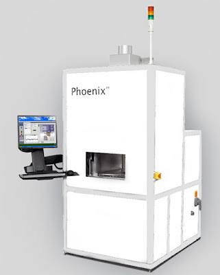
Cambridge Nanotech delivers Phoenix G2 Batch ALD system to Japan

Ultratech Cambridge NanoTech today reports that a Major Japanese manufacturer to use their  Phoenix G2 Batch Atomic Layer Deposition system for thin-film deposition on large area substrates. "The ability to deposit batch ALD solutions using ozone instead of H2O opens the door to new opportunities in several markets." Check out my previous blog on using ozon in ALD here.

SAN JOSE, Calif., June 3, 2015 /PRNewswire/ -- Ultratech, Inc. (Nasdaq: UTEK), a leading supplier of lithography, laser­ processing and inspection systems used to manufacture semiconductor devices and high­brightness LEDs (HB­ LEDs), as well as atomic layer deposition (ALD) systems, announced that its Cambridge NanoTech business unit Ultratech-CNT has delivered a new, second-generation production tool, the Phoenix G2 Batch ALD system to a major Japanese manufacturer. The system was purchased for its ability to deposit on multiple large area substrates utilizing a new, high-output oxidant source. Ultratech CNT is at the cutting-edge of nanotechnology thin-film development and leads the field with new innovations and technologies enabling it to meet the high demands of the expanding ALD market.

The company introduced the first Phoenix system in 2008 followed by enhanced models of the system in 2010. The current Phoenix G2 further expands the capabilities of the tool, and offers production-oriented safety and stability features. The Phoenix G2 thermal ALD system is a large format batch tool with flexibility to handle wafers, large planar substrates, and non-planar objects. Multiple operation modes enable manual and automated use of the system, thereby providing the end user the freedom of transitioning from research and development to production in a single platform. As a versatile, thin-film deposition technique, ALD usage is ever increasing, along with its role as an enabler in a broad spectrum of critical technologies, such as microelectronics, lighting and display, energy storage, MEMS, data storage and more. As a result, the Phoenix G2 system speeds the transition from lab-to-fab.

Ultratech Cambridge NanoTech Vice President of Global Sales, ALD Products, Bob Kane, said, "The ability to deposit batch ALD solutions using ozone instead of H2O opens the door to new opportunities in several markets. With new ALD applications emerging every week, the Phoenix G2 is designed for use in any environment from pilot to volume production with industry-leading reliability. As the leading ALD supplier to academic institutions and industrial manufacturers worldwide, Ultratech CNT will continue to develop bridge-tool solutions that implement new technologies and techniques that enable the transition from research to manufacturing environments."


Ultratech CNT's Phoenix G2 Batch ALD System

The Phoenix is engineered for high throughput and maximum uptime in any fabrication environment, from pilot production to industrial-grade manufacturing. Technologists and researchers rely on the Phoenix for repeatable, highly-accurate film deposition on flat and 3-D substrates alike. And with support for up to six individual precursor lines, the Phoenix delivers solid, liquid, or gaseous process chemistries depending on the thin film needs. The precise software control of process parameters, including temperature, flow and pressure, provide defect-free coatings on the most sensitive substrates. A compact footprint and innovative design, plus numerous automation options, makes Phoenix G2 system the practical choice for those with batch production ALD requirements. 


Wednesday, June 3, 2015

Nanopipettes for DNA detection fine tuned by ALD

Joshua Edel and his group at Imperial College London has been developing Nano pipettes [On-Demand Delivery of Single DNA Molecules Using Nanopipets]. Now they have gone a step further to fine tune the pipette for DNA dellivery and detection among other interesting things by using ALD.

Background on the group of Joshua Edel 


Analytical Sensors plays a crucial role in today’s highly demanding exploration and development of new detection strategies. Whether it be medicine, biochemistry, bioengineering, or analytical chemistry the goals are essentially the same: 

1) improve sensitivity
2) maximize throughput
3) and reduce the instrumental footprint. 

In order to address these key challenges, the analytical community has borrowed technologies and design philosophies which has been used by the semiconductor industry over the past 20 years. By doing so, key technological advances have been made which include the miniaturization of sensors and signal processing components which allows for the efficient detection of nanoscale object. One can imagine that by decreasing the dimensions of a sensor to a scale similar to that of a nanoscale object, the ultimate in sensitivity can potentially be achieved - the detection of single molecules.

Research activities within the Edel group runs at the interface between chemistry, chemical biology, physics, and medicine in order to improve and develop new classes of sensors based on these principles. As such expertise within our group includes an array of techniques and methods which includes micro and nanofabrication, material processing, surface modification chemistries, semiconductor processing and characterization techniques, confocal microscopy, plasmonics, surface enhanced Raman spectroscopy, and single molecule techniques using both optical and electrical methods.

Fine Tuning of Nanopipettes Using Atomic Layer Deposition for Single Molecule Sensing 

Jasmine Sze, Shailabh Kumar, Aleksandar P Ivanov, SAng-Hyun Oh and Joshua Edel 
Analyst, 2015,
Published online 03 Jun 2015 

 Nanopipettes are an attractive single-molecule tool for identification and characterisation of nucleic acids and proteins in solutions. They enable label-free analysis and reveal individual molecular properties, which are generally masked by ensemble averaging. Having control over the pore dimensions is vital to ensure that the dimensions of the molecules being probed match that of the pore for optimization of the signal to noise. Although nanopipettes are simple and easy to fabricate, challenges exist, especially when compared to more conventional solid-state analogues. For example, a sub-20 nm pore diameter can be difficult to fabricate and the batch-to-batch reproducibility is often poor. To improve on this limitation, atomic layer deposition (ALD) is used to deposit ultrathin layers of alumina (Al2O3) on the surface of the quartz nanopipettes enabling sub-nm tuning of the pore dimensions. Here, Al2O3 with a thickness of 8, 14 and 17 nm was deposited onto pipettes with a starting pore diameter of 75 ± 5 nm whilst a second batch had 5 and 8 nm Al2O3 deposited with a starting pore diameter of 25 ± 3 nm respectively. This highly conformal process coats both the inner and outer surfaces of pipettes and resulted in the fabrication of pore diameters as low as 7.5 nm. We show that Al2O3 modified pores do not interfere with the sensing ability of the nanopipettes and can be used for high signal-to-noise DNA detection. ALD provides a quick and efficient (batch processing) for fine-tuning nanopipettes for a broad range of applications including the detection of small biomolecules or DNA-protein interactions at the single molecule level.

Graphene oxide monolayers as atomically thin seeding layers for ALD of metal oxides

A international team of researchers from imec, MIT, BTU Cottbus and Samsung Advanced Institute of Technology have explored graphene oxide as an atomically-thin transferable seed layer for the atomic layer deposition (ALD) of dielectric materials on any substrate of choice!

Graphene oxide monolayers as atomically thin seeding layers for atomic layer deposition of metal oxides 

Amirhasan Nourbakhsh, Christoph Adelmann, Yi Song, Chang Seung Lee, Inge Asselberghs, Cedric Huyghebaert, Simone Brizzi, Massimo Tallarida, Dieter Schmeißer, Sven Van Elshocht, Marc Heyns, Jing Kong, Tomás Palacios and Stefan De Gendt 

Nanoscale, 2015, Advance Article DOI: 10.1039/C5NR01128K 
Published online 03 Jun 2015


Graphene oxide (GO) was explored as an atomically-thin transferable seed layer for the atomic layer deposition (ALD) of dielectric materials on any substrate of choice. This approach does not require specific chemical groups on the target surface to initiate ALD. This establishes GO as a unique interface which enables the growth of dielectric materials on a wide range of substrate materials and opens up numerous prospects for applications. In this work, a mild oxygen plasma treatment was used to oxidize graphene monolayers with well-controlled and tunable density of epoxide functional groups. This was confirmed by synchrotron-radiation photoelectron spectroscopy. In addition, density functional theory calculations were carried out on representative epoxidized graphene monolayer models to correlate the capacitive properties of GO with its electronic structure. Capacitance–voltage measurements showed that the capacitive behavior of Al2O3/GO depends on the oxidation level of GO. Finally, GO was successfully used as an ALD seed layer for the deposition of Al2O3 on chemically inert single layer graphene, resulting in high performance top-gated field-effect transistors.