Saturday, September 24, 2016

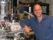
Arthur del Prado 1931-2016

(In brief, from www.asm.com) Arthur del Prado, ASMI's founder and former CEO, played a fundamental and founding role in the semiconductor industry. He globally is viewed as a legend within our industry and his legacy extends from Silicon Valley to Tokyo.

 Arthur del Prado (www.asm.com)

In 1996, ASM International was publicly-listed on the AEX in Amsterdam. Under Del Prado's leadership, it acquired Finnish company Microchemistry (1999) and Korean group Genitech (2004), cementing its position as market leader in atomic layer deposition (ALD).

Arthur del Prado died peacefully at his home on September 9, 2016. He is rightly recognized as the father of the European semiconductor equipment industry. Indeed, it is impossible to imagine today's industry without him.

Please find the amazing story about Arthur del Prado and ASM International here. ​​​​


Friday, September 23, 2016

Rumor: Apple 2017 iPhone may have Samsung's new Flexible OLED made by ALD

Here are some unconfirmed information that ALD will be used in the next generation Apple iPhone as of 2017.In addition, Korea IT News is claiming that both Samsung and LG have finalized the R&D phase of introducing ALD barrier technology for OLED and are now working closely with Korean ALD OEMs to go to production. Companies mentioned are Jusung Engineering, WONIK IPS, AP System, and TES.

With Apple reportedly shifting to iPhones with OLED displays starting in 2017, it will be interesting to see if Apple will be using Samsung's latest OLED technology that may be ready for the 2017 anniversary iPhone. According to a new OLED report, Samsung Display and LG Display are working to introduce ALD (Atomic Layer Deposition) technology to flexible OLED thin-film encapsulation process. They both have worked closely with their equipment partners to get them up to speed. ALD technology will add an important component to OLED displays for smartphones that add protecting organic materials from oxygen and water that will increase the overall life of a display. Samsung in particular is reported to be "working fast to introduce ALD technology." 
LINK: http://www.patentlyapple.com/patently-apple/2016/09/apples-2017-iphone-may-use-samsungs-new-flexible-oled-atomic-layer-deposition-technology.html

Checking the Korean ALD companies on the stockmarket give no hint or reaction that any of them are about to sign big deals.


Last 6 months performance for an index based on Korean companies with ALD Technology that may be used for OLED Encapsulation. Tes Co Ltd, Jusung Engineering Co., Ltd., EugeneTechnology Co Ltd and Wonik IPS Co Ltd. (Plotted using Google Finance)

The second Belux workshop is organized the 17th and 18th November 2016 at imec

The second Belux workshop is organized the 17th and 18th November 2016 at imec in Belgium with the objective to spark synergy between modeling, deposition and characterization of emerging transition metal compounds for next generation technologies. Innovative materials are expected to enable novel device concepts and breakthrough ideas for future logic and memory applications. 
More about this event is to be found under: http://www2.imec.be/be_en/education/conferences/belux2/home.html.

Materials of interest for workshop include:
• Advanced ferromagnetic materials, including high PMA materials and Heusler alloys.
• Strongly correlated transition metal oxides, including Mott materials.
• Novel dielectrics for microelectronics, including dielectrics for resistive memory and flash devices.
• Novel lead-free and/or HfO2-based ferroelectric materials.
• Chalcogenide glasses for selector devices.
• Two-dimensional transition metal dichalcogenides (e.g. MoS2).


Areas of interest:
• Deposition: novel precursors and processes, growth surface dependencies, impact of process parameters on the layer properties.
• Characterization: phase formation, interface characterization, optical characteristics, stress characterization, magnetic properties, stress formation, material defectivity.
• Modeling: theoretical calculations such as DFT to improve the understanding of precursor reactivity, deposition or material properties.
• Chemical etching and surface functionalization of chalcogenide compounds.
The workshop consists of a combination of presentations and posters.

COST Action MP1402 - HERALD

Hooking together European research in Atomic Layer Deposition

Thursday, September 22, 2016

Applied Materials to grow in 3DNAND, Logic and Materials based patterning

Applied Materials Expects higher wafer fab equipment (WFE) spending driven by :
  • multi-year inflections including 3D NAND,10 and 7 nanometer logic and foundry, 
  • materials-based patterning
  • new factory investments in China Outlines plans to drive 50 percent growth in display business to $1.8 billion by FY2019
NEW YORK, Sept. 21, 2016 (GLOBE NEWSWIRE) -- At its 2016 Analyst Day, Applied Materials, Inc. detailed its innovation leadership strategy to drive sustainable growth and announced target non-GAAP adjusted earnings per share of $2.45 to $3.17 for fiscal 2019, with a midpoint of $2.80. This would represent compound earnings growth of approximately 17 percent over the next three years.

Wednesday, September 21, 2016

Sub-100 nm features seamless roller mold using anodization and ALD for R2R nanoimprint lithography

Here is a really cool open access paper form A*STAR on using direct anodization and ALD to prepare a sub-100 nm seamless roller mold for roll-to-roll nanoimprinting. The ALD after the  Al roller mold was deposited with  TiO films in a home-built ALD setup at 150 °C using TiCl4 and water.

LK Tan, AYY Ho - Journal of Vacuum Science & Technology B, 2016 - scitation.aip.org 3 days ago - The authors demonstrate an approach using direct anodization and atomic  layer deposition (ALD) to prepare a sub-100 nm seamless roller mold for roll-to-roll nanoimprinting. In this approach, the roller mold is prepared by direct anodization of a ...

Saturday, September 17, 2016

EpiValence to exhibit at the joint Euro CVD-Baltic ALD 11-14 June in Linköping, Sweden

On behalf of the CVD and ALD research community we are very happy to announce EpiValance from the UK as exhibitor at the joint Euro CVD-Baltic ALD 11-14 June in Linköping, Sweden.


EpiValence is a highly focussed manufacturer of select niche chemicals, dedicated to providing the highest quality products and services on a Global basis to meet customer requirements now and in the future. Our continuing success is founded on three principles: uncompromising commitment to the highest standards of product quality, purity, and consistency; the establishment and maintenance of genuinely interactive relationships with customers; and a leading-edge, proactive approach to the rapidly evolving electronics market globally.


Thursday, September 15, 2016

GLOBALFOUNDRIES details 7nm FinFET Technology Offering

The table below was recently published on SemiWiki and today Globalfoundries announced their 7 nm time line in a press release below. Judging by the comparison TSMC is now in lead of Moore´s Law trailed by Intel, Samsung and Globalfoundries.

"The platform is based on an industry-standard FinFET transistor architecture and optical lithography, with EUV compatibility at key levels." This means that EUV may be inserted in some BEOL metallization layers and the rest of the patterning like the complete fronte end FinFET will be made by ALD multiple patterning... oh yeah and some etch and immersion lithography in between.

CompanyCurrent20162017201820192020
Global Foundries16.6nmNANA9.5nmNANA
Intel13.4nmNA9.5nmNANA6.7nm
Samsung16.6nm12.0nmNA8.4nmNANA
TSMC18.3nm11.3nm8.2nmNA5.2nmNA


Standard Node Value by Year (edited on 9/15) according to SemiWiki (LINK)


Santa Clara, Calif., September 15, 2016 – GLOBALFOUNDRIES today announced plans to deliver a new leading-edge 7nm FinFET semiconductor technology that will offer the ultimate in performance for the next era of computing applications. This technology provides more processing power for data centers, networking, premium mobile processors, and deep learning applications.


GLOBALFOUNDRIES’ new 7nm FinFET technology is expected to deliver more than twice the logic density and a 30 percent performance boost compared to today’s 16/14nm foundry FinFET offerings. The platform is based on an industry-standard FinFET transistor architecture and optical lithography, with EUV compatibility at key levels. This approach will accelerate the production ramp through significant re-use of tools and processes from the company’s 14nm FinFET technology, which is currently in volume production at its Fab 8 campus in Saratoga County, N.Y. GLOBALFOUNDRIES plans to make an additional mutli-billion dollar investment in Fab 8 to enable development and production for 7nm FinFET.

Wednesday, September 14, 2016

Oxford Instrument to present how to shape a Plasma in ALD at BALD2016 in Russia

Agnes Kurek from Oxford Instrument in collaboration with TU Eindhoven to present insights into how to shape a Plasma in ALD at BALD2016 in Russia. The BALD 2016 will be held at the Solo Sokos Hotel Palace Bridge in St. Petersburg (Russia) from October 2nd to 4th, 2016.

Plasma ALD of SiO2, NiO and HfO2 on the FlexAL System: Modifying Flow, Pressure and Plasma Parameters

Atomic layer deposition (ALD) of ultra-thin oxide films is interesting for many applications including photovoltaics [1], optics [2], and microelectronics [3]. For a robust plasma ALD process, the elements of flow, pressure and plasma conditions must be carefully balanced to achieve good reproducibility. In this work, the effects of these parameters on the following newly- developed ALD processes will be discussed.
Remote plasma & thermal ALD in one flexible tool
Silicon dioxide films have been demonstrated by plasma ALD using bis(tert-butylimino)silane (BTBAS) and oxygen plasma. The combination of a high working pressure controlled by a quick-action APC valve with the rapid pumping of a turbomolecular pump, has increased the film deposition rate (nm/min), and growth per cycle, without compromising film quality in terms of electrical and optical properties. This process is robust, repeatable and conformal on high aspect ratio structures, up to 30:1.

Basic set up of the FlexAL system including optional in-situ ellipsometry
Nickel oxide films have been demonstrated by plasma ALD, using nickelocene and oxygen plasma. Rapid bubbling of the precursor delivers efficient dosing, while low pressure O2 plasma allows for fast surface saturation and good uniformity.

Hafnium oxide films have been demonstrated by plasma ALD using tetrakis(dimethylamido)hafnium (TDMAH) and oxygen plasma. This results in improved deposition uniformity over tetrakis (ethylmethylamido) hafnium (TEMAH), even at short cycle times. Electrical characterisation of resultant HfO2 films will be discussed.

In general, the important parameters for plasma ALD of SiO2, NiO and HfO2 will be discussed, focusing on the effect of flow and pressure for each process step.

[1] G. Dingemans, C. A. A. van Helvoirt, D. Pierreux, W. Keuning, W. M. M. Kessels, E.C.S. 3 (2012) H277.
[2] T.S. Yang, W. Cho, M. Kim, K.-S. An, T.-M. Chung, C. G. Kim, Y. Kim, J. Vac. Sci. Technol. A 4 (2005) 1238.
[3] A. Colon, J. Shi, Solid-State Electronics 99 (2014) 25.

ALD protects luminescent quantum dots

Researchers from Saint Louis, USA, protects CdTe quantum dots from oxidation by using alumina shells synthesized by ALD. The recnte resutlts have been published in Chemical Communications (Chem. Commun., 2016, Advance Article DOI: 10.1039/C6CC05090E)

ALD coated quantum dots (figure released by Royal Society of Chemistry, License Number: 3947440205944 , Chem. Commun., 2016, Advance Article DOI: 10.1039/C6CC05090E)

Background:

Applications of luminescent quantum dots require the materials to be stable under a wide range of temperatures, photon fluxes and chemicfial environments. The researchers from St Lois demonstrate that Al2O3 shells synthesized by atomic layer deposition on films of CdTe quantum dots are effective to prevent chemical degradation for up to 17 hours under continuous illumination at 90 °C in ambient air. 

ALD was carried out in a custom hot wall reactor and more information can be found in the free to download supplementary information (here).
 

Tuesday, September 13, 2016

Plasma Electronic form Germany new sponsors of the BALD Engineering News Blog

I am very happy to announce that Plasma Electronic from Germany is now a sponsor of the BALD Engineering ALD News Blog. I met with Plasma Electronic during the ALD2016 Ireland conference end of July and hope to hear more about there progress with their wafer based PEALD reactor (see picture below) and other plasma processing technologies. One of the next chances to meet with Plasma Electronic will be at the Euro CVD-Baltic ALD 2017 Exhibition in Sweden next summer. Also you may check their news services here for additional announcements and exhibitions : http://www.plasma-electronics.com/news.html


Plasma Electronic at the ALD2016 Ireland exhibition demonstrating their PEALD technology to the conference delegates.

Plasma Electronic is specialized on the planning, design, construction and marketing of plasma treatment devices. The focus is the activation and fine cleaning of surfaces and the coating of surfaces with the technologies PECVD, PVD, PEALD and their combinations. In their laboratory they are able to measure and analyze properties of coatings like hardness, coating thickness, surface energy and surface tension.

The facility has a production area of 1000 m² enabling us to construct all sizes of plasma devices. The plasma chamber sizes vary from 10 liters in research and development devices up to 8000 liters in devices for mass production.

Plasma Electronic has developed a variety of processes for different applications. They can be used to remove residues of organic or silicone pollution (
Plasmaclean©), for better wettability and adhesion (Actiplas©), for permanently hydrophilic (Aquacer©) or hydrophobic (Lipocer©) coatings, for hard coatings with low wear and low friction (Carbocer©), for transparent protection and "anti-fingerprint" coatings (Clearprotect©) and for decorative coatings (Decocer©).

Plasma Electronics ALD Offerings

FinFET Fundamentals by Lam Research

Lam Research has published a tutorial on FinFETs basics that is very interesting for anyone who likes to understands the basics of FinFETs:

Transistors are at the heart of our cherished electronics. Millions, or even billions, of these tiny switches go to work for us when we check our mobile phones, use our computers, start our automobiles, or play on our gaming consoles. But what exactly are transistors and how do they work? And how have they changed over the years? Here we take a look at some transistor fundamentals, including the operation of a field-effect transistor (FET), as well as the FinFET technology inflection that is enabling even smaller, more powerful semiconductor chips.
Link to tutorial here.

Monday, September 12, 2016

Major memory manufacturer qualifies AIXTRON’s QXP-8300 mini-batch ALD system

AIXTRON reaches important milestone for its silicon semiconductor manufacturing technology

AIXTRON SE (FSE: AIXA; NASDAQ: AIXG), a worldwide leading provider of advanced deposition equipment to the semiconductor industry, announced today that a major memory manufacturer has qualified its

 QXP-8300 Atomic Layer Deposition (ALD) mini-batch system (www.aixtron.com)

QXP-8300 Atomic Layer Deposition (ALD) mini-batch system suitable for high-k oxide films in various advanced memory applications including 3D structure devices. 

“We are delighted that our customer has completed the evaluation of our QXP-8300 ALD system for the manufacturing of the most advanced high performance memory devices. The QXP-8300 ALD system enables the manufacturing of advanced films with excellent electrical and device properties. AIXTRON is looking forward to further support its customer’s memory development plans by providing the production equipment to address the challenges of a rapidly evolving industry,” says Bill Bentinck, Vice President and General Manager of AIXTRON Inc., USA. 

As the semiconductor memory cell size continues to be scaled down, manufacturers need advanced technologies for the deposition of precise layers of dielectric, metal and non-volatile memory materials. AIXTRON’s QXP-8300 ALD system includes the patented TriJet vaporizer technology integrated with the unique close coupled showerhead design that enables the use of low vapor pressure precursors as needed in making higher-k dielectrics and metal nitrides for the performance improvement.

Sunday, September 11, 2016

Atomic Level Processing at SEMICON Europa in Grenoble

As usual at SEMICON Europa there will be many presentations given on ALD and Atomic Level Processing. This year SEMICON is running in Grenoble and Tuesday will be a busy day for all ALD guys. First there is the annual ALD Symposium now rebranded as "Symposium of The ALD Lab Saxony - Workshop on Atomic Layer Processing". Then in the afternoon Hessel Spray from ASM International takes over the show and chairs the Advanced Materials Session in the Tech Arena.

See below for more details on each event! 

Symposium of the ALD Lab Saxony

Workshop on Atomic Layer Processing


Date: 25 October 2016
Time: 9:00–13:00
Location: Le Bans

Pleas get in contact with Prof Bartha and Christoph Hossbach at IHM TU Dresden for more information about this event.

Web : http://www.semiconeuropa.org/ald-lab
ALD Lab Saxony : http://www.ald-lab-saxony.de/

Advanced Materials Session

Date: 25 Oct 2016
Time: 14:00–17:00
Location: TechARENA 2


Agenda

Chair Hessel Sprey, Manager European Cooperative Programs and External R&D, ASM International
14:00 Introduction
14:05
Molecular self-assembly from liquids on atomically flat surfaces: from fundamentals to applications
  Brandon Hirsch, postdoctoral researcher, KU Leuven
14:30
2D and graphene - Status of the Graphene Flagship and the potential applications
  Kari Hjelt, Head of Innovation, Graphene Flagship / Chalmers University
14:55
Advanced materials processing with ALD and CVD precursors
  Jean-marc Girard, CTO, Air Liquide
15:20
III-V selective area growth on Si: from Logic to Photonic applications
  Clement Merckling, Principle Scientist, imec
15:45
Hot-Wire Assisted ALD: From Idea to Realization
  Alexey Kovalgin, Associate Professor, MESA+ Institute For Nanotechnology, University of Twente
16:10
Atomic Layer Deposition and Etching of Thin Films - Research and Application
  Christoph Hossbach, Senior Scientist, Technische Universität Dresden
16:35
Development of block copolymers to create complex
  Michael Morris, Director, AMBER Research Centre, AMBER, Trinity College Dublin
17:00 Closing
  Johan Dekoster, Program Manager, imec
17:05 END

Globalfoundries Fab 1 Dresden to start 12 nm FDSOI enabled by double patterning

Here is good news for the Globalfoundries Fab1 in Dresden and the many people I know working there! Fab1 has already successfully ramped 22 nm FDSOI by using Double Patterning in combination with Immersion lithography and will now according to a statement by Gregg Bartlett, senior vice president of the CMOS Platform Business Unit at GlobalFoundries continue with the same technology for 12 nm FDSOI:

When it comes to the patterning in lithography, “it’s very analogous on 22nm,” Bartlett said. The 22nm FD-SOI process involves double patterning, with two metal layers, and that’s the plan for 12nm, as well. “No triple patterning.” [Semiconductor Engineering]

PEALD is typically employed for double patterning this could mean some extra business for the OEMs supplying single wafer PEALD like ASM Internationals Eagle XP8 platform, which is also capable of PECVD that may be used for spacer/liner applications. Please find more details on the 12 nm FDSOI news below.

GLOBALFOUNDRIES unveiled a new 12 nm FD-SOI semiconductor technology, extending its leadership position by offering the industry’s first multi-node FD-SOI roadmap. Building on the success of its 22FDX™ offering, the company’s next-generation 12FDX™ platform is designed to enable the intelligent systems of tomorrow across a range of applications, from mobile computing and 5G connectivity to artificial intelligence and autonomous vehicles.

 Globalfoundries Fab1 in Dresden Germany (Wikipedia)

Thursday, September 8, 2016

Harvard University ALD-prepared TiO2 nanofin planar lens for high res imaging

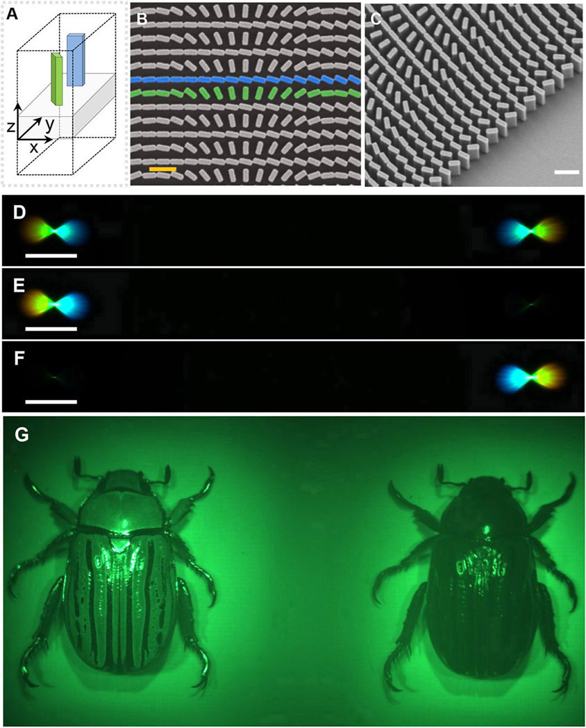
Researchers at Harvard University have developed a metasurface platform for visible wavelengths based on ALD-prepared TiO2 nanofins. By doing so they can fabricate a metalens for high-resolution imaging with a planar and compact configuration. Fabrication is made by using a simple one-step lithography integration ensures a high-performance and versatile platform that could find many applications in optics, ranging from imaging and spectroscopy to laser-fabrication processes.
 Please find here the full story in SPIE Newsroom.

Fab Equipment Spending Ascending according to SEMI

The Fab Equipment Spending is ascending according to a report that SEMI’s Industry Research and Statistics group has published its August update of the World Fab Forecast report.

Fab Equipment Spending by Quarter (SEMI)

The largest growth drivers according to the reporty are 3D NAND and Logic 10nm/7nm for mobile devices and future IoT devices - obviously fully loaded with numerous ALD process steps!

Continue here for the full story.

Beneq to sponsor & exhibit at Euro CVD - Baltic ALD 2017

Fantastic News - We just confirmed that we signed on Finnish ALD and Display Manufacturing Company Beneq as a Gold Sponsor & Exhibitor at Euro CVD - Baltic ALD 2017. Their finacial contribution will help us craete a fanatstic even for the CVD and ALD research and industry communty. Beneq will also have acces to a meeting roome for interaction with their customers & research community.


CVD-ALD bonanza that will take place in Linköping, Sweden 11-14 june, 2017. We will organize a joint EuroCVD-BalticALD meeting over three packed days including a 4th day Tutorial and welcome mixer on Sunday evening. 
 
 
Sponsorship negotiations at ALD2016 Ireland with Beneq. (Photo Katharina Knaut Fotographie )

Sponsors & Exhibitors

please contact Henrik Pedersen (henrik.pedersen@liu.se) or Jonas Sundqvist (jonas.sundqvist@baldengineering.com) for sponsoring and to take part in exhibition of this event! 


Modular flow and Plasma Electronic from Germany to Exhibit at EuroCVD - Baltic ALD 2017

We are very happy to annonc that modular flow and Plasma Electronic from Germany to Exhibit at EuroCVD - Baltic ALD 2017 in Linköping Sweden 11-14 Junde 2017.

Please contatc us if you like to join the exhibition!

Henreik Pedersen (henrik.pedersen@liu.se)
Jonas Sundqvist (jonas.sundqvist@baldengineering.com)


Aug 15, 2016 ... modularflow launches mini ALD reactor with integrated QCM ... modularflow mini ALD Dimensions with 3 precursor sources: approx. 420 x 260 ...

Atomic layer deposition for two-dimensional materials (ALDfor2D) workshop

The aim of this one-day workshop is to give an overview of current topics in the field of atomic layer deposition (ALD) for the synthesis and integration of 2D Materials such as graphene and the transition metal dichalchalcogenides for nanodevice applications. The workshop is geared towards both scientists who work in the field as well as newcomers and technologists who want to get an overview of the field. The workshop is organized in the context of the COST action "HERALD" (MP1402).

Key facts

Date: October 31, 2016
Location: Eindhoven, The Netherlands
Participation: Free
Registration & more details: http://nanomanufacturing.nl/2DWorkshop/

Invited speakers

  • Prof. Robert Wallace (University of Texas at Dallas, USA)
  • Prof. Kim (Yonsei University, South Korea)
  • Dr. Annelies Delabie (IMEC, Belgium)
  • Dr. Ravi Sundaram (OIPT, UK)
  • More to follow!

The workshop is sponsored by

Tuesday, September 6, 2016

Lam Research - New Atomic Layer Etching Capability Enables Continued Device Scaling

As published by Lam Research : With the introduction of Lam’s latest Flex™ dielectric etch system, we have expanded our atomic layer etching (ALE) portfolio to include both conductor and dielectric etch. At the 10 nm technology node and beyond, conventional technologies do not provide sufficient control for the stringent specifications demanded. As described in our recent announcement , this newest Flex product delivers the atomic-level control needed for manufacturing advanced logic devices and is first in the industry to use dielectric ALE in high-volume production.

 
Lam Research introduce their latest Flex™ dielectric etch system today! The new product will expand their atomic layer etching (ALE) portfolio to include both conductor and dielectric etch, and is the first in the industry to use dielectric ALE in high-volume production. (Lam Research at LinkedIn)

Announcement for HERALD Early Career Investigators (ECIs)

To promote the next generation of ALD scientists and help them to establish themselves as research leaders in the ALD community, we have formed a network within HERALD for Early Career Investigators (ECIs). Broadening out the COST definition of ECI, we welcome investigators from within a year of submitting their PhD dissertation to PhD+10 years - however, these are not strict limits.


Our ambition is to run workshops where we meet to exchange ideas on career moves, grant applications and possible collaborations. In 2017 we are planning to organize a kickoff event at the Joint EuroCVD-BalticALD conference in Linköping 11-14 June, and a stand-alone workshop where we also invite some senior ALD scientists to give advice on how to establish oneself as an ALD scientist.

If you are interested in joining this network, please contact one of us. 
Henrik Pedersen, henrik.pedersen@liu.se
Jolien Dendooven, jolien.dendooven@ugent.be
Ville Miikkulainen, ville.miikkulainen@helsinki.fi
Adrie Mackus, a.j.m.mackus@tue.nl

High-throughput Large-Area Spatial ALD by Beneq from Finland

Beneq announced their new fast Spatial ALD reactor in November last year (Beneq introduces the next revolution in industrial ALD). End of July Beneq released more information in the ALD2016 Ireland exhibition

Large-area sheet-to-sheet spatial ALD system (From Beneq Blog)

Beneq is a pioneer in ALD solutions that enable coating of large substrates, and we have also discussed them here in the blog. Beneq’s Mikko Söderlund was showcasing our innovations in this area to the ALD2016 audience.

Our large-area spatial ALD coating equipment has been developed for high-throughput coating applications such as Zn buffer for CIGS solar cells, OLED encapsulation, glass coating, and rear-surface passivation of crystalline solar cells. The new spatial ALD process makes it possible to coat bigger substrates faster and in a more flexible way. The capacity of the new large-area ALD coating equipment really opens doors to new possibilities in industrial-level coating. You can check the latest results of our large-sheet ALD tests from Mikko’s poster.


The large area spatial ALD reactor from Beneq (picture from Beneq)

The above deposition speeds result in massive area throughput figures. For rear-surface passivation (with a thin 5 nm Al2O3 coating) as a case example, processing wafers at substrate speeds exceeding 20 m/min would allow a single piece of equipment to produce over 30 000 wafers per hour. That is fast by any standard. (from Beneq Blog)

Download Mikko's ALD2016 poster to get all the details of the latest spatial ALD pilots with large substrates.


I met with Beneq at the ALD2016 Exhibition to discuss the new spatial ALD reactor (Picture Fotografie Katharina Knaut).


Monday, September 5, 2016

ALD Financials: Applied Materials and Lam Research - Head to head ...

Here is an interesting head to head comparison by Seeking Alpha between the two leading Equipment Manufacturers in Semiconductor industry - Applied Materials and Lam Research. Neither have until now considering the opportunities and resources that they had been that successful in ALD. 

The big mystery  - Applied Materials is actually dominating much of all : Epi, PVD, Implant, CMP, RTP and CD-SEM businesses, but has only like 2% of the ALD Market and Etch is also not looking that good. So it will be interesting to follow how the new Olympia platform takes on the competition.

Most inserting, while the OEM market a sa whole is concentrated into the Top 5 players (Applied Materials, Lam Research, ASML, Tokyo Electron and KLA-Tencor) that all together has a market share of  >70% ALD ist totally different. Here the sub Top 5 players constitute >65% of the market (ASMI, Kokusai, Jusung, Aixtron, Picosun, Ultratec, Beneq, Oxford Instruments, NCD and others).

Table 1 - AMAT and LRCX Shares for Etch and Deposition (PECVD)
Etch ($M) 2012 Revenues Share 2015 Revenues Share
Applied Materials 395 10% 1,130 18%
Lam Research 1,745 45% 3,250 52%
Total Market 3,840
6,250


PECVD ($M) 2012 Revenues Share 2015 Revenues Share
Applied Materials 700 55% 1,070 57%
Lam Research 430 34% 600 32%
Total Market 1,275
1,880


Total Etch-Deposition 2012 Revenues Share 2015 Revenues Share
Applied Materials 1,095 21% 2,200 27%
Lam Research 2,175 43% 3,850 47%
Total Market 5,115
8,130


Source: The Information Network (theinformationnet.com)


US and Korean Researchers Making pristine graphene in a microwave oven

Nanotechweb.org reports : Researchers at Rutgers University in the US and UNIST in Korea have succeeded in producing high-quality graphene by simply zapping graphene oxide with microwaves for 1–2 seconds. The new technique produces pristine graphene that has an electron mobility as high as 1500 cm2/V/s when made into field-effect transistors with graphene as the channel material. This is among the highest value ever obtained from reduced graphene oxide materials.
 
 
 Continue reading here.
 

Thursday, September 1, 2016

Sandia ALD bubble membrane can capture CO2 and reduce emissions efficiently

(Nanowerk News) Sandia National Laboratories and the University of New Mexico (UNM) have created a powerful new way to capture carbon dioxide from coal- and gas-fired electricity plants with a bubble-like membrane that harnesses the power of nature to reduce CO2 emissions efficiently.

The membrane can be manufactured by PEALD (Link).

 
By combining a water droplet loaded with CO2 enzymes in an ultrathin nanopore on a flexible substrate, researchers at Sandia National Laboratories realized the first technology that meets and exceeds DOE targets for cost-effective CO2 capture. When compared with the nearest membrane competitor, this technology delivers a three times permeation rate, twenty times higher selectivity, and ten time lower fabrication cost. The CO2 Memzyme has the potential to remove 90% of CO2 emissions and is forecasted to save the U.S. coal industry $90 billion a year compared to conventional technology. (Sandia Youtube)

DARPA Researchers Develop Novel Method for Room-Temperature ALD

Successful deposition of silicon and gallium nitride at low temperature could allow three-dimensional control of thin films and integration of previously incompatible microelectronics materials.

DARPA-supported researchers have developed a new approach for synthesizing ultrathin materials at room temperature—a breakthrough over industrial approaches that have demanded temperatures of 800 degrees Celsius or more. The advance opens a path to creating a host of previously unattainable thin-film microelectronics, whose production by conventional methods has been impossible because many components lose their critical functions when subjected to high temperatures. 
 

Pictured is a Gallium Nitride film deposited on a Silicon substrate at 27 degrees Celsius (80 degrees Fahrenheit) using an innovative process for depositing super thin films. Current deposition methods for these materials require temperatures around 800 degrees Celsius (1,472 degrees Fahrenheit), which is incompatible with microelectronics processing due to the damage that heat can wreak on underlying substrate materials.This new method could allow integration of previously incompatible microelectronics materials. (University of Colorado Boulder image)
 
The new method, known as electron-enhanced atomic layer deposition (EE-ALD), was recently developed at the University of Colorado, Boulder (CU) as part of DARPA’s Local Control of Materials Synthesis (LoCo) program. The CU team demonstrated room-temperature deposition of silicon and gallium nitride—linchpin elements in many advanced microelectronics—as well as the ability to controllably etch specific materials, leading to precise spatial control in three dimensions. Such a capability is critical as the demand grows for ever-smaller device architectures.

After first demonstrating the process in early 2015, team members went on to perform detailed mechanistic studies to learn how best to exploit and control EE-ALD for film growth. By controlling the electron energy during the ALD cycles, they discovered that they could tune the process to favor either material deposition or removal. The ability to selectively remove (etch) deposited material with electrons under conditions as low as room temperature is unprecedented and is anticipated to enhance film quality. The group is also exploring other methods to etch specific materials—such as aluminum nitride and hafnium oxide, important in specialized electronics applications—showing that they can selectively etch these materials in composites, which provides an attractive alternative to traditional masking approaches.

CU has also built a custom deposition chamber to demonstrate industrial relevance and scalability of the EE-ALD process, which can deposit or etch films composed of multiple materials on industrial-scale six-inch silicon wafers. In principle, the method could be scaled to larger substrates and parallelized to process many wafers at once. The researchers are now working to understand the vast parameter space of the EE-ALD process to better control film composition and properties in three dimensions.

“Looking forward, the EE-ALD approach could serve not just as a tool for integrating incompatible materials but also more generally to build and etch device architectures at atomic scales, an increasingly important capability as circuit geometries shrink,” said Tyler McQuade, DARPA program manager.

CU’s work, which was performed in collaboration with the Naval Research Laboratory and National Institute of Standards and Technology, was recently recognized as one of six “Highlights of 2016”—selected from more than 400 accepted oral presentations and posters at the 16th International Conference on Atomic Layer Deposition in Dublin, Ireland.

Electron enhanced atomic layer deposition (EE-ALD) of silicon films at room temperature
Jaclyn Sprenger1, Huaxing Sun1, Andrew Cavanagh*1, Steven George1,2
1University of Colorado, Department of Chemistry and Biochemistry, USA, 2University of Colorado, Department of Mechanical Engineering, USA

Wednesday, August 31, 2016

RASIRC Renews Funding for Atomic Layer Deposition Research at University of California, San Diego (UCSD)

RASIRC renewed its funding agreement with the University of California, San Diego (UCSD) for on-going semiconductor processing research. Professor Andrew Kummel of the Department of Chemistry represents UCSD in this agreement. The gift donation supports one student for one year. RASIRC made a similar gift donation last year. RASIRC manufactures BRUTE® hydrogen peroxide and hydrazine vaporizers for emerging ALD applications.

San Diego, CA, August 31, 2016 (Newswire.com) - RASIRC announced today that it has renewed its funding agreement with the University of California, San Diego (UCSD) for on-going semiconductor processing research. Professor Andrew Kummel of the Department of Chemistry represents UCSD in this agreement. The gift donation supports one student for one year. RASIRC made a similar gift donation last year. RASIRC manufactures BRUTE® hydrogen peroxide and hydrazine vaporizers for emerging ALD applications. 
“Our ongoing research focuses on solving difficult materials problems associated with emerging semiconductor technology,” said Professor Kummel. “Financial and technical support from RASIRC aids our efforts to create new films and passivation layers for continuous shrinkage of semiconductor devices.”

As part of the agreement, RASIRC provides BRUTE® Peroxide and BRUTE Hydrazine materials for experimentation. The UCSD team produced and published significant findings from these materials during the previous year of research. Chemists and engineers from both organizations regularly collaborate on research and share their findings. Research covers passivation of SiGe channel materials and development of new low temperature deposition methods for metal nitrides.

“Universities play a critical role in chemical and materials research behind advances in the semiconductor industry as shown by the results produced and published by UCSD over the past year,” said  Daniel Alvarez, RASIRC Chief Technology Officer. “UCSD is a great partner and we look forward to working with the team to perfect novel new chemistries that solve very difficult problems where traditional methods do not work.”

Professor Kummel’s group is focused on understanding and imaging chemical processing at the atomic level.  Current projects include (1) In-situ cleaning and functionalization of SiGe, Ge, and InGaAs semiconductors for defect-free interfaces on FinFET sidewalls and contacts;  (2) Selective etching and ALD on semiconductors and insulators; (3) Non-Covalent Functionalization of two-dimensional semiconductors; (4) Nano-scale synthesis of silica nanoshells for tumor ultrasound imaging and ablation. Additional detail on the Kummel Research Group can be found at http://kummelgroup.ucsd.edu.

NCD to deliver Lucida GD series ALD system for OLED encapsulation with Chinese display manufacturer, TIANMA

NCD reports today (8/31 2016) :The OLED market is going to prospect fast gigantic growing in the near future because OLED has the possibilities of bending, folding and various forms like circle, therefore it will be applied for flexible and wearable devices. Flexible OLEDs need excellent thin encapsulation layers in order to keep the property from the permeation of water and oxygen under the external environment using repeated bending, folding and rolling of devices. However, the current encapsulation based on PECVD is not satisfied with future flexible OLEDs, so new encapsulation technology would absolutely be required.

Many OLED manufactures are currently reviewing to use ALD technology because of obtaining the highest property from the encapsulation layers of OLED, but they have not been solving the low throughput and particle issues followed by using their ALD systems.

In order to clear these problems, NCD has completed to develop the 6th ALD equipment for thin film encapsulation which satisfies high quality, large area and high throughput applying for the inventive ALD technology, and we have been also continuously testing customer’s samples. NCD’s ALD encapsulation layer shows much better properties than that of PECVD, and the encapsulation capability on application for foldable products has been confirmed from the customers. As a result, NCD has recently entered into the contract with Chinese display manufacturer, TIANMA to supply the 5.5th generation class ALD system of Lucida GD series for thin film encapsulation of OLED. It apparently shows that NCD’s core technologies and the result of developments have been approved by the oversea customer.

NCD will keep doing our best to set Lucida GD series as the standard of all of flexible OLED encapsulation equipment with this achievement and become the number one global ALD Company with the best competitiveness making new challenges and developments.

Lucida™ GD Series ALD


High throughput atomic layer deposition system for OLED displays 


Cluster system for Lucida™ GD series


Applications

  • Barrier layer(Al2O3, TiO2) for flexible substrate
  • WVTR(water vapor transmission rate) 5.3x10⁻⁵g/m2·day (tritiated water test @30nm Al2O3/PEN substrate)
  • Encapsulation layer(Al2O3,TiO2) for OLED
  • Applications of mass-product

Benefits

  • High throughput : > 30 panels/hour
  • Substrate size : > 6G (1500 x 1850mm2)

Features

  • Advanced process kit and small volume chamber for short gas cycle times
  • Extremely materialize ALD mechanism
  • Small foot print
  • Totally integrated process module
  • Easy process control

Technical specifications