Tuesday, October 30, 2018

Estimating rising demand for Ru thin-films in the next generation chips

STREM Chemicals offers one of the most promising ruthenium amidinate precursors for growing Ru ALD or CVD films

The saturation of Moore’s curve while following systematic downscaling of logic and memory devices has given rise to the biggest challenges involving contacts and interconnects in the chip. The transistors (FinFETs at leading nodes) are getting better and better at smaller dimensions. On the contrary, the shrinking interconnects and contacts at each technology node cause the unwanted resistance-capacitance (RC) delay to increase. Therefore, the chipmakers are exploring new materials to replace conventional tungsten and copper for contacts and interconnects, respectively (see figure below, LINK). At 10 nm, Intel switched over to cobalt for contacts and some, but not all, interconnect layers. Ru is also being explored hugely since Co has some trade-offs as well as higher line resistance (VLSI 2017, Globalfoundries). In fact, there was also news in the market regarding use of Ru implemented in Intel’s 10 nm technology node (TechInsight 2018).
Intel 10nm mid end of line cobalt and copper 12 layer metallization as presented at IEDM December 2017 pre-announcement (LINK, Press kit).

Ru is also an excellent candidate for the electrode capacitor in DRAM applications and gate electrode material in CMOS transistor applications because of its high melting point, high oxidation resistance, and low resistivity. Ruthenium’s lower resistivity and ease of dry etching give it a significant advantage over other noble metals like iridium and platinum. Ru seed-layer deposited as a conformal via liner significantly improves copper adhesion and hinders oxygen diffusion in interconnects and through-silicon-via (TSV) applications. Moreover, ruthenium oxide is conductive and therefore, oxygen diffusion from adjacent materials or processes does not hinder the device performance. Recent research reports the use of ruthenium-based materials as an electrode in ferroelectric applications as well.

Thus, as the main bottleneck of next generation ICs, interconnects and contacts are nowadays the major driving factors of the market of high quality specialty chemicals for the performance or function specific materials or molecules. The physical and chemical properties of a single molecule or a formulated mixture of molecules as well as its chemical composition influence the end product performance extensively. Therefore, unlike the other sub-sectors of the chemical industry, the companies manufacturing and marketing specialty chemicals provide more often than not targeted customer service to innovative individual technical solutions for their customers. 

Since 1964, Strem Chemicals, Inc. has been serving its clients from academic, industrial and government research and development laboratories as well as commercial scale businesses in the pharmaceutical, microelectronic and chemical / petrochemical industries. Strem (Headquarters: Newburyport, Massachusetts, USA) is a high purity specialty chemicals’ manufacturer and supplier. Strem also provides custom synthesis (including high pressure synthesis) and current good manufacturing practice (cGMP) services. With ISO 9001 certification for Quality Management System (QMS) standard and documentation, most of the Strem’s products are reliably of high purity, typically 99%, with some at 99.9999% metals purity. Strem utilizes a comprehensive range of analytical techniques tailored to each product to insure quality because the researchers typically rely on the supplier's quality procedures and documentation, which may kill a great research idea if poorly conducted. All of Strem's catalogs, since inception, have listed “Color and Form” for every product as primary indicators of quality.

More than fifty years of experience in manufacturing inorganic and organometallic chemicals has enabled Stem to expand its product offering of MOCVD, CVD, and ALD precursors. They are continually adding new products for this dynamic and exciting field. Strem’s product range includes:


Most of the available Ru ALD or CVD precursors have issues concerning low vapor pressure and high impurity levels, such as carbon and oxygen, which get incorporated in the films. In addition to that, long incubation times impacting throughput and process controllability, poor film adherence, and non-uniformity in high-aspect ratio structures are some critical limitations of the field. However, ruthenium amidinate precursors such as Bis(N,N’-di-t-butylacetamidinato)ruthenium(II) dicarbonyl (catalog number 44-0056) and others are some of the most promising precursors finding a home in Strem’s product catalog for growing ALD and CVD films. Each amidinate ligand chelates the metal center through two metal-nitrogen bonds. These relatively weak M-N bonds and strong byproduct N-H bonds lead to lower ALD growth temperatures. However, the M-N bonds are strong enough to provide stability to the precursor at the standard temperatures used. Also, since the amidinate ligands chelate to the metal center, they are thermally stable yet have high and self-limited reactivity to water vapor which is essential for ALD. Amidinates do not have any oxygen-metal bonds thus enabling the deposition of metallic films with very low oxygen content in the film and at the interface with the sub-layer.

ALD thin-films deposited using Bis(N,N’-di-t-butylacetamidinato)ruthenium(II) dicarbonyl exhibit high conductivity, density and purity.  Atomic probe microscopy measurements revealed nearly carbon free crystallites with far less carbon impurity segregated near the grain boundaries. The films also showed very good conformality even inside the trenches with aspect ratios (~40:1) possessing strong adhesion. The precursor was found to be thermally stable in a bubbler at 130°C for months and showed very clean TGA vaporization with only trace residue (0.2%).
---
Promotional Blog for Strem Chemicals, Inc.
Researched, produced & written by BALD Engineering AB, Stockholm, 2018-10-30
Abhishekkumar Thakur, Jonas Sundqvist
www.baldengineering.com


Video Online - HYCOAT Workshop "Hybrid nanocoatings through molecular layer deposition"

Here is a fantastic set of ALD Tutorials & Presentations available on YouTube from a recent HYCOAT event at Ghent University, Belgium August 27-29, 2018 - HYCOAT Workshop "Hybrid nanocoatings through molecular layer deposition (LINK). Please find the YouTube streams below.

HYCOAT Workshop "Hybrid nanocoatings through molecular layer deposition (Picture from Press release LINK)


HYCOAT is a project funded by the European Union in the framework of the H2020 Marie Skłodowska Curie Actions – Innovative Training Networks. It is the first European Training Network at the intersection of chemistry, physics, materials science and engineering dealing with the synthesis and applications of hybrid coatings grown by Molecular Layer Deposition (MLD). On its YouTube Channel, you can find content from the Workshops organized within the HYCOAT training network, as well as information on the research conducted at the participating universities and research institutes.


An introduction to atomic layer deposition (ALD) by Professor Christophe Detavernier, Ghent University, Belgium at the HYCOAT Workshop "Hybrid nanocoatings through molecular layer deposition". (August 27-29, 2018 at Ghent University, Belgium)


Dr. Paul Poodt from TNO, Netherlands, presenting ALD/MLD reactor consepts and design at the "Hybrid nanocoatings through molecular layer deposition" workshop held on August 27th - August 29th, 2018, Ghent University, Belgium.


Professor Adrie Mackus from Eindhoven University of Technology, Netherlands with a lecture on area-selective ALD at the HYCOAT Workshop "Hybrid nanocoatings through molecular layer deposition", held between August 27th and August 29th, 2018 at Ghent University, Belgium.


Professor Mikko Ritala from University of Helsinki, Finland giving an introduction to the chemistry of ALD/MLD precursors at the HYCOAT Workshop "Hybrid nanocoatings through molecular layer deposition", held between August 27th and August 29th, 2018 at Ghent University, Belgium. 


Professor Jess Jur from North Carolina State University, U.S.A. presenting the basics and latest research on atomic layer deposition onto polymers and textiles at the "Hybrid nanocoatings through molecular layer deposition"workshop (August 27-29, 2018, Ghent University, Belgium)

An introduction to diffusion phenomena occuring during atomic layer deposition processing by Professor Mato Knez, CIC nanoGUNE, Spain. Presented at the "Hybrid nanocoatings through molecular layer deposition" workshop held at Ghent University, Belgium from August 27th to August 29th, 2018.


Dr. Karen Leus, Ghent University, Belgium, giving an introduction on properties and applications of metal-organic frameworks and covalent organic frameworks at the "Hybrid nanocoatings through molecular layer deposition" workshop at Ghent University, Belgium.

Monday, October 29, 2018

ALD/MLD reactor design and precursor delivery Tutorial by Paul Poodt

Dr. Paul Poodt from TNO, Netherlands, presenting ALD/MLD reactor consepts and design at the "Hybrid nanocoatings through molecular layer deposition" workshop held on August 27th - August 29th, 2018, Ghent University, Belgium.


Argonne scientists create new oil-resistant filter technology

Argonne reports a novel new way to keep oil from clogging filters and equipment using ALD coated mabranes.

Crude oil is sticky stuff and often clogs filters membranes and other equipment used in the oil and gas industry. To address this problem, scientists at the U.S. Department of Energy’s (DOE) Argonne National Laboratory have developed a novel approach, which will prolong the lifetime of key industrial equipment.
The scientists used a method called atomic layer deposition, which uses chemical vapors to deposit a very thin coating of the metal oxide on all of the filter membrane surfaces. They experimented using different metal oxides on off-the-shelf commercial polymer membranes to find which ones worked the best. The team published the results in ACS Nano on August 14. 


This shows a membrane, when fouled by crude oil, but coated by titanium dioxide (TiO2), releases oil when placed in water.

Read the full news release here: https://www.anl.gov/article/argonne-s...

Coventor - N7 FinFET Self-Aligned Quadruple Patterning Modeling

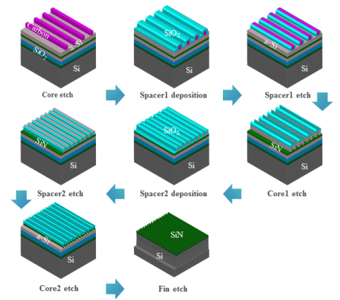
Coventor just released a white paper for ther modelling on FinFET Self-Aligned Quadruple Patterning for the 7nm node (N7).

You can request the paper for download here: LINK

White Paper : N7 FinFET Self-Aligned Quadruple Patterning Modeling

In this paper, we model fin pitch walk based on a process flow simulation using the Coventor SEMulator3D virtual platform. A taper angle of the fin core is introduced into the model to provide good agreement with silicon data. The impact on various Self-Aligned Quadruple Patterning process steps is assessed. Etch sensitivity to pattern density is reproduced in the model and provides insight on the effect of fin height variability.


Sunday, October 28, 2018

TECHCET Critical Materials Reports(TM) and Market Briefs on CVD & ALD

TECHCET CA LLC is an advisory services firm focused on materials supply-chain market analysis and technologies for electronic device markets. Now integrated with the Critical Material Council (CMC), TECHCET works with leading IC fabricators to solve supply-chain issues by way of CMC activities, Critical Material Reports™ (CMRs), Analyst meetings, and other services. Favorite topics include Silicon wafers, ALD/CVD precursors, CMP consumables, Gases, Photoresists, Metals/chemicals, Wet chemicals and China.


Jonas Sundqvist, Ph.D. – Sr. Technology Analyst of TECHCET— covers ALD and CVD precursors and related technologies, and is the co-chair of the Critical Materials Council (CMC) Conference. His over 20 years of work experience includes group leader of the High-k devices group at Fraunhofer’s Center Nanoelectronic Technologies (CNT), which included 28nm node work for GLOBALFOUNDRIES Fab1. While there, he founded the ALD Lab Dresden together with TU Dresden. At Infineon Memory Development Centre (MDC) he developed high-k and metal nitride ALD processes, and at Qimonda he was a materials manager focused on the ALD / CVD precursors supply-chain. He is the founder of BALD Engineering, an independent blog and networking platform for ALD. He holds a Ph.D. and a M.S. in inorganic chemistry from Uppsala University, Sweden, a B.S. in electrical and electronics engineering from Lars Kagg, and nine patents.

CVD/ALD High K Metal Precursors – NEW!

The High K / ALD Metal Precursors report provides information on the applications and markets associated with front end and back end of line precursors used to produce high dielectric constant (K) dielectrics and atomic layer deposition metal oxides and nitrides.

Dielectric Precursors 2018 – Just Released!

The Dielectric Precursors Report provide detailed market, supply chain and technology trend information required for anyone developing strategy for their business, be it a materials supplier or semiconductor chip manufacturer. Precursor types include, gapfill, ILD, low K, and multi-patterning.

Market Briefs – Precursor Bulk Delivery Systems

Coming Soon – Detailed report about the precursor bulk delivery systems

Market Briefs – Precursor Development – ALD / CVD Systems and Precursors

The report details about the Precursor Development in ALD/CVD Systems and Precursors

Market Briefs – Precursor Development – How to take a precursor from lab to fab

Coming Soon – The precursor development briefing explains all about how to take it from lab to fab.
GET THE REPORT

Market Briefs - China ALD / CVD Market

Coming Soon

For additional information about CMRs or CMC membership please contact us by clicking here,  call +1-480-332-8336, x 1, or go to www.techcet.com or www.cmcfabs.org.

SAVE the DATE for the 2019 CMC Conference, scheduled for April 25-26 in the Malta/Albany, New York area.

Fabrication of buried nanostructures with flat surface by ALD


Fabrication of buried nanostructures by atomic layer deposition (Open Access)

Rizwan Ali, Muhammad Rizwan Saleem, Matthieu Roussey, Jari Turunen & Seppo Honkanen Scientific Reportsvolume 8, Article number: 15098 (2018) 

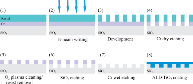
We present a method for fabricating buried nanostructures by growing a dielectric cover layer on a corrugated surface profile by atomic layer deposition of TiO2. Selecting appropriate process parameters, the conformal growth of TiO2 results in a smooth, nearly flat-top surface of the structure. Such a hard surface can be easily cleaned without damage, making the nanostructure reusable after contamination. The technique has wide applicability in resonance-domain diffractive optics and in realization of quasi-planar metamaterials. We discuss design issues of such optical elements and demonstrate the method by fabricating narrow-band spectral filters based on the guided-mode resonance effect. These elements have strong potential for, e.g., sensing applications in harsh conditions.


Fabrication process of ALD-TiO2 buried guided mode resonance filters (GMRFs). Shared under Creative Commons Attribution 4.0 International License From: Fabrication of buried nanostructures by atomic layer deposition


Drexel enables a Lithium-Sulfur battery evolution

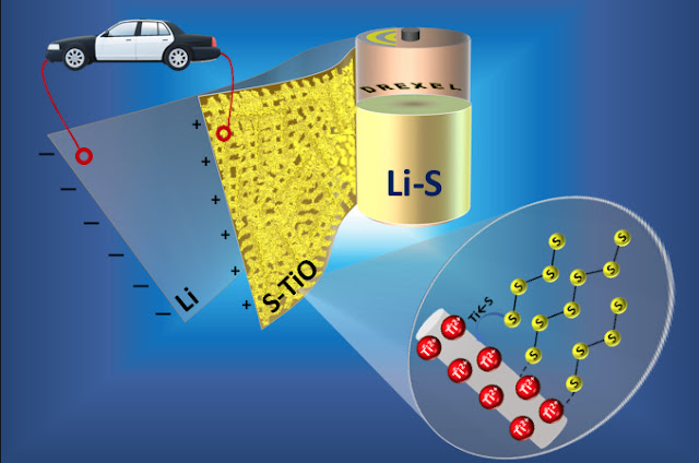
Drexel’s College of Engineering reports that researchers and the industry are looking at Li-S batteries to eventually replace Li-ion batteries because a new chemistry that theoretically allows more energy to be packed into a single battery This improved capacity, on the order of 5-10 times that of Li-ion batteries, equates to a longer run time for batteries between charges.

However, the problem is that Li-S batteries have trouble maintaining their superiority beyond just a few recharge cycles. But a solution to that problem may have been found with new research.

The new approach, reported by in a recent edition of the American Chemical Society journal Applied Materials and Interfaces, shows that it can hold polysulfides in place, maintaining the battery’s impressive stamina, while reducing the overall weight and the time required to produce them.

Lithium-sulfur batteries could be the energy storage devices of the future, if they can get past a chemical phenomenon that reduces their endurance. Drexel researchers have reported a method for making a sulfur cathode that could preserve the batteries' exceptional performance. (Image from Drexel News)

Saturday, October 27, 2018

Area-selective ALD using Si precursors as inhibitors

Area-Selective Atomic Layer Deposition Using Si Precursors as Inhibitors

Rizwan Khan, Bonggeun Shong, Byeong Guk Ko, Jae Kwang Lee, Hyunsoo Lee, Jeong Young Park, Il-Kwon Oh, Shimeles Shumi Raya, Hyun Min Hong, Kwun-Bum Chung, Erik J. Luber, Yoon-Seok Kim, Chul-Ho Lee, Woo-Hee Kim, and Han-Bo-Ram Lee

Chem. Mater., Article ASAP
DOI: 10.1021/acs.chemmater.8b02774

Short-chain aminosilanes, namely, bis(N,N-dimethylamino)dimethylsilane (DMADMS) and (N,N-dimethylamino)trimethylsilane (DMATMS), have been used as Si precursors for atomic layer deposition (ALD) of SiO2. In this work, the DMADMS and DMATMS Si precursors are utilized as inhibitors for area-selective ALD (AS-ALD). The inhibitors selectively adsorb on a SiO2 surface but not on H–Si, so that SiO2 becomes selectively deactivated toward subsequent ALD. The deactivation of the SiO2 surface by the inhibitors was investigated using various experimental and theoretical methods, including surface potential measurements, spectroscopic ellipsometry, and X-ray photoelectron spectroscopy. Better inhibition was observed for ALD of Ru and Pt than for ALD of Al2O3 and HfO2. Through quantum mechanical and stochastic simulations, the difference in the blocking ability for noble metal and metal oxide ALD by the aminosilane inhibitors could be attributed to the inherently partial surface coverage by the inhibitors at their saturation and the reactivity of the subsequent ALD precursors. As silane inhibitors can be easily integrated with vacuum-based processes to facilitate high volume manufacturing of upcoming electronic devices, the current study provides a potential approach for the utilization of AS-ALD in pattern fabrication inside 3D nanostructures.


"Reprinted with permission from (DOI: 10.1021/acs.chemmater.8b02774). Copyright (2018) American Chemical Society."

Friday, October 26, 2018

$70m lab for next-generation semiconductors at National University of Singapore with Applied Materials

 Picosun ALD Tool in the NUS clean room
 
[NUS News LINK] NUS and Applied Materials — the world’s top semiconductor and display equipment company, and a leader in materials engineering solutions — have jointly established the Applied Materials-NUS Advanced Materials Corporate Lab, supported by the National Research Foundation (NRF). This $70 million collaboration, Applied Materials’ first university-based research laboratory, will focus on research and development (R&D) with the aim of developing and quickly commercialising innovative materials for manufacturing next-generation semiconductors.
From left: Vice President & Regional President (SEA) of Applied Materials Mr Brian Tan, Dr Raja, Mr Heng, NUS Chairman Mr Hsieh Fu Hua, NRF CEO Prof Low Teck Seng and Prof Tan officially launching the laboratory
Materials engineering has helped enable major advancements in semiconductor devices over the years, said Dr Prabu Raja, Senior Vice President at Applied Materials. “However, new applications in artificial intelligence require orders of magnitude improvements in chip performance and power efficiency. Materials innovation will have a critically important role in achieving these improvements,” he noted in his speech at the official launch of the laboratory on 25 October.


Thursday, October 25, 2018

NCD contracted to supply new ALD equipment for production of µ-OLED with LG Display

Korean ALD equipment manufacturer, NCD reports new order of µ-OLED ALD equipment from LG Display

"NCD has recently contracted with LGD to supply µ-OLED manufacture equipment which is new Lucida GuD Series for Al2O3-ALD encapsulation to avoid OLED degradation induced water and oxygen. Newly introduced Lucida GuD is high volume batch-type ALD equipment based on the process and hardware of OLED encapsulation technology of Lucida GD Series.

µ-OLED produced by this system is micro display with high resolution for augmented reality(AR) and virtual reality(VR) and has been expected the huge application and market in the future.

Otherwise, manufacture of µ-OLED requests high productivity like display industry therefore ALD tools with high film quality and low throughput for Semiconductor couldn’t meet the need of the customers and the market. So NCD is more expecting that this µ-OLED is next growth engine market because it has high volume ALD equipment and excellent OLED encapsulation technology.

NCD will lead µ-OLED ALD equipment market with this starting point and continue to make efforts to become the world’s best specialized ALD technology company.”


LucidaTM GuD Series


Patterned films by atomic layer deposition using Parafilm as a mask

Recently I have worked a lot with etch people. These guys are definitely a completely different breed from us ALD people. and I have gotten a bit annoyed of their obsession in using Capton Tape all the time. It is rather annoying to cut perfect pieces and then try to separate the protective film on the double sided sticky tape and then it is alos very tedious to clean up after you exposed it to a plasma with nasty gases. Now there is an alternative worth testing also for etch process development!  And for sure - ALD guys are behind it once again saving the etchers and Litho people like we did for multiple patterning.
Here is a very practical and low cost method for all of you who have the need to depositing patterned films by ALD or protect the substrate or certain areas from ALD film growth like the back side or edge. Zhang et al for University of Helsinki has investigated using Parafilm as a mask to block the film growth on selected areas of the substrate surface. Interestingly it works also well above the melting temperature of Parafilm (60 °C) since parfin in this form is very viscous up to the range 275 to 300 °C, below which quite many ALD processes produce high quality films.


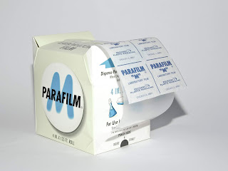
A box of parafilm (From Wikimedia Commons, the free media repository)
On an interesting side note, the researchers from Helsinki has actually an Ir-ALD based device on board of the Mercury space ship BepiColombo heading towards the planet as we speak. According to Prof. Ritala [LINK] it is a ALD-Ir coated microchannel plate for x-ray focusing. However if this device had any Parafilm patterning involved in the making I do not know. Anyway in about 7 years we all look forward to see some results from the Satellite using high class Ir-ALD from Helsinki.
The study concludes:
  • The use of Parafilm as a blocking mask is a simple, clean and effective method for ALD film patterning.
  • The blocking ability was tested for ALD of Al2O3, TiO2 and Ir.
  • The Parafilm method works up to 275 °C but above 300°C the melted film will flow on vertical samples
  • Outgasing from the Parafilm at elevated temperatures may hinder growth around the edge of the Parafilm (observed for TiO2 and Ir ALD).
  • Potential use of the method besides R&D is seen for protecting contact areas in IC and MEMS

Patterned films by atomic layer deposition using Parafilm as a mask

Zhang, Chao ; Kalliomäki, Jesse ; Leskelä, Markku ; Ritala, Mikko
Journal of Vacuum Science & Technology A: Vacuum, Surfaces, and Films, January 2018, Vol.36(1)
https://avs.scitation.org/doi/abs/10.1116/1.5001033

This paper presents a new method for depositing patterned films by atomic layer deposition (ALD) using Parafilm as a mask to block the film growth on selected areas of the substrate surface. This offers an easy and efficient method for large area patterning from the millimeter to even meter scale as needed, for example, for protecting contact areas in integrated circuits and microelectromechanical system devices and in preventing film growth on the backside of substrates. It is shown here that Parafilm can protect the substrate against Al2O3, TiO2, and Ir film growth effectively. However, outgassing from the Parafilm affects the film growth on the unmasked areas differently for the three materials. For Al2O3, there are no significant effects on the growth rate and film quality on the nonmasked areas and the thickness profiles next to the Parafilm masked areas are narrow. For TiO2 and Ir, by contrast, the thickness profiles are wider and outgassing also slows down the Ir growth. Energy dispersive x-ray analysis confirms that Ir does not grow on Parafilm. Al2O3 and TiO2 films do grow on Parafilm, but after the ALD process, the Parafilm can be peeled off easily with tweezers and the areas under the Parafilm mask are without any deposition.

Tuesday, October 23, 2018

Imec and ASML Enter Next Stage of EUV Lithography Collaboration

Intensified collaboration will advance high-volume production with current EUV lithography and develop future EUV systems

LEUVEN (Belgium) & VELDHOVEN (The Netherlands), OCTOBER 22, 2018 (LINK) —Today, world-leading research and innovation hub in nanoelectronics and digital technologies imec, and ASML Holding N.V. (ASML), the technology and market leader in lithographic equipment, announce the next step in their extensive collaboration. Together, they will accelerate the adoption of EUV lithography for high-volume production, including the current latest available equipment for EUV (0.33 Numerical Aperture, NA). Moreover, they will explore the potential of the next-generation high-NA EUV lithography to enable printing of even smaller nanoscale devices advancing semiconductor scaling towards the post 3 nanometer Logic node. To this end, they will establish a joint high-NA EUV research lab.

Imec and ASML have been conducting joint research for almost thirty years. In 2014, they created a joint research center, the Advanced Patterning Center, to optimize lithography technology for advanced CMOS integration and to prepare the ecosystem to support advance patterning requirements. Now, they bring this cooperation to the next stage with the installation of ASML’s most advanced and high-volume production dedicated EUV scanner (NXE:3400B) in imec’s cleanroom. Utilizing imec’s infrastructure and advanced technology platforms, imec and ASML researchers and partner companies can pro-actively analyze and solve technical challenges such as defects, reliability and yield, and as such accelerate the EUV technology’s industrialization.

Monday, October 22, 2018

Shaanxi Kuntech launch flexible semiconductor service manufacturing Base Project

OLED-Info reports: The press conference for the landing and launching of Shaanxi Kuntech Flexible Semiconductor Service Manufacturing Base Project was grandly held in West Fengxi New City, West Xian Xin New District, Shaanxi province on the morning of October 16, with its theme being Shinning Shaanxi and Shaping the Future World".

Kuntech is the first high-end enterprise in China that focuses on the development and autonomy of flexible semiconductors and advanced display technologies. It develops and actively accumulates intellectual property with the highest intensity focus technology, and achieves technology autonomy and freedom to operate. Facing the huge challenges of future display and semiconductor development, Kuntech Semiconductor continues to innovate and advance in the field of flexible semiconductor display through a series of revolutionary technologies.

It is reported that Shaanxi Kuntech flexible semiconductor service manufacturing base is a major science and technology industry project of Shaanxi Province, China. The total investment of the project is 6 billion USD. The project includes a world-class flexible semiconductor and display technology R&D certification center, a strong and complete flexible semiconductor and display industry chain, and the sixth-generation flexible AMOLED demonstration production line with its production capacity being 30K large substrates per month, featuring three major processes (array, AMOLED EL, flexible module). The size of the substrate is 1500mmx1850mm.
Full story : OLED-Info LINK


Saturday, October 20, 2018

HERALD 3rd ECI workshop: Science communication and mapping a future road for ECIs

[HERALD LINK] Specialized training in science communication and networking for the ECI members and guests, by Dr. Simon Elliott and Dr Fergus McAuliffe(open session)

NETWORKING WITH HEAPS OF CHARM
  • What makes a good networker memorable?
  • How do they seem so carefree and engaging?
  • How do they keep the conversation going in those awkward moments of silence?
This hands-on interactive workshop focusses on our ability to communicate your research and work interests clearly and effectively across many audience types. We delve into body language and active listening to engage different audiences, in either group or networking situations. We share coping mechanisms to survive awkward or challenging interactions. Using theatre games and role-playing exercises, this workshop helps you distill your message, craft a short sharp pitch about what you do and provide you with the tools to keep conversation going.

- Group training session in RoadMapping the future of ALD research in Europe, working with the output of HERALD summit 2018 to find future roads for the ECI community
- Open ECI session, with focus on peer to peer interaction


Dates: 8 Nov 2018 to 9 Nov 2018
Address: Institute of Electrical Engineering SAS Bratislava Slovakia
URL: http://www.elu.sav.sk/en/contact/

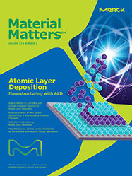
Materials Matters (TM) topical issue on Atomic Layer Deposition

Here is a Materials Matters(TM) topical issue on Atomic Layer Deposition with interesting papers on ALD - especially the one on Group 11 metals. That is ALD of copper, silver and gold by Prof. Barry.

Materials Matters(TM) - Atomic Layer Deposition - Nanomanufacturing with ALD (LINK)
  • NANOCOMPOSITE COATINGS with Tunable Properties Prepared by Atomic Layer Deposition
  • SILICON NITRIDE ATOMIC LAYER DEPOSITION: A Brief Review of Precursor Chemistry
  • GROUP 11 THIN FILMS by Atomic Layer Deposition
  • FEW MONOLAYER ATOMIC LAYER DEPOSITION on Surfaces and Interfaces for Energy Applications


The 4th International Conference on ALD Applications & 2018 China ALD Conference

[www.c-ald.com] This week the 4th International Conference on ALD Applications & 2018 China ALD Conference was held  in Shenzhen, China, from October 14 to 17, 2018.

The four-day meeting was dedicated to the fundamentals and applications of Atomic Layer Deposition (ALD) technology in various fields.This conference will feature plenary sessions, oral sessions, poster sessions and industrial exhibitions.

PROCEEDING AND FULL PAPER:

Full contributed papers will be peer reviewed and published in a special issue Nanoscale Research Letters ((2018 impact factor: 3.125) https://nanoscalereslett.springeropen.com/aald


Samsung Electronics Starts Production of EUV-based 7nm LPP Process

[SAMSUNG news.samsung.com] Samsung Electronics, a world leader in advanced semiconductor technology, today announced that it has completed all process technology development and has started wafer production of its revolutionary process node, 7LPP, the 7-nanometer (nm) LPP (Low Power Plus) with extreme ultraviolet (EUV) lithography technology. The introduction of 7LPP is a clear demonstration of Samsung Foundry’s technology roadmap evolution and provides customers with a definite path to 3nm.

The commercialization of its newest process node, 7LPP gives customers the ability to build a full range of exciting new products that will push the boundaries of applications such as 5G, Artificial Intelligence, Enterprise and Hyperscale Datacenter, IoT, Automotive, and Networking.

“With the introduction of its EUV process node, Samsung has led a quiet revolution in the semiconductor industry,” said Charlie Bae, executive vice president of foundry sales and marketing team at Samsung Electronics. “This fundamental shift in how wafers are manufactured gives our customers the opportunity to significantly improve their products’ time to market with superior throughput, reduced layers, and better yields. We’re confident that 7LPP will be an optimal choice not only for mobile and HPC, but also for a wide range of cutting-edge applications.”

Tuesday, October 9, 2018

Picosun launches new PicoMEDICAL™ solutions specially targeted for healthcare industries

ESPOO, Finland, 9th October 2018 – Picosun Group, a leading, global provider of ALD (Atomic Layer Deposition) thin film coating technology, strengthens its position in the healthcare market with new PicoMEDICAL™ solutions specially developed for the needs of medical device manufacturers. 
ALD technology has the potential to disrupt the whole field of healthcare industries. Ultra-thin, biocompatible and bioactive ALD films manufactured with Picosun’s production ALD equipment already encapsulate surgical implants and improve their adhesion to bone. This speeds up the healing process and protects the patient from possible metal ion leakage from the implant into the body. In pharmaceutical industries, Picosun’s powder ALD technology is used to functionalize the surface of drug particles for controlled drug delivery.

Friday, October 5, 2018

Sequential Infiltration Synthesis - SIS