Wednesday, April 11, 2018

RASIRC Presents Alternative Method for Aperture Oxidation in VCSELs

San Diego, Calif – April 11, 2018–RASIRC announced today that the company will present at VCSEL Day 2018, held April 12-13, 2018 in Ulm, Germany. Jeffrey Spiegelman, RASIRC President and Founder, will present an alternative method for aperture oxidation. The annual event provides a European forum to discuss the state of the art and latest research. “Wafer to wafer and batch to batch oxidation uniformity are difficult challenges in VCSEL manufacturing,” said Mr. Spiegelman. “The use of an additional and stronger oxidant such as hydrogen peroxide gas with or without water vapor is an attractive approach. This can provide an additional control parameter in order to optimize uniformity for higher yields.” 


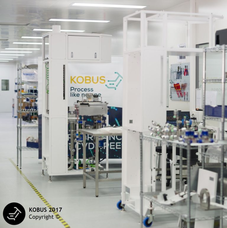
RASIRC Peroxidizer® for High Concentration H2O2 Gas (left) and RASIRC BRUTE™ Peroxide for Ultra-Dry H2O2 Gas (right) please find more information here (LINK)
VCSELs are specialized laser-emitting semiconductors that are used in a wide variety of applications. VCSEL yield is directly related to the control during oxidation of aperture structure. Researchers have been challenged to identify additional methods to ensure uniformity. RASIRC has developed an innovative alternative that can provide better control of oxidation rate by adjustments in hydrogen peroxide concentration as well as lower process temperatures.

RASIRC’s Peroxidizer® and Hydrogen Peroxide Steamer (HPS) products provide high volumes of reactive H2O2/H2O mixtures for high throughput oxidation processes. These reactive gas generators are ideal for batch furnaces by providing the ability to vary concentration and flow rate, with or without the use of a carrier gas. Delivery into sub-atmospheric conditions is an additional feature.

RASIRC products also include the RainMaker Humidification System (RHS) that generates high precision water vapor for oxidation applications. This product has already proven to be useful in VCSEL manufacturing.

About RASIRC

RASIRC specializes in products that generate and deliver gas to fabrication processes. Each unit is a dynamic gas plant in a box—converting common liquid chemistries into safe and reliable gas flow for most processes. First to generate ultra-high purity (UHP) steam from de-ionized water, RASIRC technology can now also deliver hydrogen peroxide gas and hydrazine gas in controlled, repeatable concentrations. RASIRC gas delivery systems, humidifiers, and closed loop humidification systems are critical for many applications in semiconductor, photovoltaic, pharmaceutical, medical, biological, fuel cell, and power industries. Call 858-259-1220, email info@rasirc.com or visit http://www.rasirc.com.

Contacts:
RASIRC
Jeffrey Spiegelman
Phone: 858-259-1220
E-mail: jeff@rasirc.com

Tuesday, April 10, 2018

AVS Short Course Webinar on Atomic Layer Etching (ALE) June 13,2018


Atomic Layer Etching (ALE):
June 13,2018
REGISTRATION DEADLINE: June 11, 2018
The AVS Short Course Webinar focusing on Atomic Layer Etching (ALE) will be held on Wednesday, June 13, 2018 from 1:00-5:00 p.m (EDT). This webinar will be taught by Steven M. George, Professor in the Dept. of Chemistry & Biochemistry and Dept. of Mechanical Engineering, University of Colorado at Boulder. This AVS Webinar on ALE will provide the training required to understand plasma-assisted ALE and thermal ALE. The webinar will explain the process strategies for plasma-assisted ALE and thermal ALE. Important ALE approaches for many materials including Si, SiO2, Al2O3, TiN and W will be described that are useful for advanced semiconductor processing.

Who should attend: Scientists, engineers and technicians who use or plan to use atomic layer etching for atomic scale fabrication.

Syllabus: Learn More

Date: June 13, 2018

Time: 1:00-5:00 p.m. (EDT)

Cost: $200/person

REGISTRATION DEADLINE: June 11, 2018


Questions: E-mail heather@avs.org or call 530-896-0477.

Sunday, April 8, 2018

ALD on Porous Materials: Problems with Conventional Approaches to Catalyst and Fuel Cell Electrode Preparation

The last two years I have been conducting some ALD and CVD on powder and started to follow that literature segment. Here is a most recent paper (Open Access) with a lot of practical information for all of you hands-on ALD people to test in the lab (or the fab God forbid...).

Atomic Layer Deposition on Porous Materials: Problems with Conventional Approaches to Catalyst and Fuel Cell Electrode Preparation


Tzia Ming Onn 1, Rainer Küngas 2, Paolo Fornasiero 3, Kevin Huang 4 and Raymond J. Gorte
Inorganics 2018, 6(1), 34; doi:10.3390/inorganics6010034

Atomic layer deposition (ALD) offers exciting possibilities for controlling the structure and composition of surfaces on the atomic scale in heterogeneous catalysts and solid oxide fuel cell (SOFC) electrodes. However, while ALD procedures and equipment are well developed for applications involving flat surfaces, the conditions required for ALD in porous materials with a large surface area need to be very different. The materials (e.g., rare earths and other functional oxides) that are of interest for catalytic applications will also be different. For flat surfaces, rapid cycling, enabled by high carrier-gas flow rates, is necessary in order to rapidly grow thicker films. By contrast, ALD films in porous materials rarely need to be more than 1 nm thick. The elimination of diffusion gradients, efficient use of precursors, and ligand removal with less reactive precursors are the major factors that need to be controlled. In this review, criteria will be outlined for the successful use of ALD in porous materials. Examples of opportunities for using ALD to modify heterogeneous catalysts and SOFC electrodes will be given. View Full-Text 


Saturday, April 7, 2018

Plasma-Therm acquires KOBUS and F.A.S.T ALD & CVD hybride technology

KOBUS, an innovative French company based in Grenoble that has brought a new faster ALD-like technology to production level  has been acquired by US Plasma-Therm. The technology is called F.A.S.T, an alternative to ALD where thick and conformal films are required like e.g. TSV and 3D chip integration or MEMS. F.A.S.T. stands for “Fast Atomic Sequential Technology and is enabled by a innovative CVD reactor design combined with fast pulsing capability. KOBUS has focused on solutions for 3D integration challenges, which fits good to the Plasma-Therms etch and PECVD product portfolio. Plasma-Therm also recently acquired the small Swedish plasma etch/dep OEM Advanced Vacuum who target back-end applications and reverse engineering etchers.

ST. PETERSBURG, Florida (April 4, 2018) — Plasma-Therm today announced that it has acquired KOBUS, an innovative plasma deposition company, which enables F.A.S.T®, a valuable alternative to ALD where thick and conformal films are required.

This unique deposition method is at the crossroads of ALD and CVD: F.A.S.T. stands for “Fast Atomic .Sequential Technology.” F.A.S.T. is enabled by proprietary CVD reactor design combined with pulsing capability, and while capable of depositing in traditional ALD mode, it is optimal for thick and conformal layer deposition and offers new solutions for 3D integration challenges.
Production of the 3rd generation of F.A.S.T. process modules at KOBUS (wwww.kobus-tech.com)

KOBUS offers a unique portfolio of equipment for both mature and advanced materials deposition, which merges well with Plasma-Therm’s operation, expanding the plasma-based deposition and etch suite of products for all silicon and compound semiconductor emerging applications.

This acquisition will allow Plasma-Therm to establish a solid base in Europe and conduct R&D development in the Grenoble “Silicon Valley,” a region fueled with R&D, startups and large semiconductor corporations.

About Plasma-Therm
Plasma-Therm LLC is a manufacturer of leading plasma etch, deposition, and advanced packaging equipment for specialty semiconductor and nanotechnology markets. Plasma-Therm's plasma-processing and advanced-packaging solutions are used in research, pilot manufacturing, and volume production of wireless, photonics, solid state lighting, MEMS/NEMS, data storage and other devices. Learn more at http://www.plasmatherm.com

Thursday, April 5, 2018

FREE webinar: Optimising ALD high-k oxides for novel applications

FREE webinar: Optimising ALD high-k oxides for novel applications, 19 April 2018, 15:50 UTC [LINK]


Dr Harm Knoops and special guest speaker, Dr Uwe Schroeder, Deputy Scientific Director from NaMLab GmbH Dresden, Germany, will talk you through the ALD of ferroelectric HfO2 for novel memory applications and the tuning properties of TiO2 and HfO2 by substrate biasing during Plasma ALD.

The webinar will comprise of two talks, with a Q&A session at the end. Register here


Dr.ir. Knoops is the Atomic Scale Segment Specialist  for Oxford Instruments Plasma Technology and holds a part-time researcher position at the Eindhoven University of Technology. His work covers the fields of (plasma-based) synthesis of thin films, advanced diagnostics and understanding and developing plasma ALD and similar techniques. His main goals are to improve and advance ALD processes and applications for Oxford Instruments and its customers. He has authored and co-authored more than 30 technical papers in peer-reviewed journals.  

Dr Uwe Schroeder has held the Deputy Scientific Director position at NaMLab GmbH, Dresden, Germany since 2009. His main research topics are material properties of ferroelectric hafnium oxide and the integration of the material into future devices.

Prior to joining NaMLab, Schroeder was in a Senior Staff Scientist position at Qimonda, previously known as Infineon Technologies (Memory Division) and Siemens Semiconductor before.  At Infineon’s Memory Development Center in Dresden, his research included work on high k dielectric and its integration into DRAM capacitors as a project manager. During this work the so far unknown ferroelectric properties of doped HfO2 based dielectrics were found. He focused on a detailed understanding of these new material properties and their integration into memory devices. 

Schroeder received a Master degree in Physics and a PhD degree in Physical Chemistry field from University of Bonn, Germany including a research visit at UC California, Berkeley and worked at University of Chicago as a post-doctoral researcher.

Wednesday, April 4, 2018

Call for Papers ALD for perovskite-based devices - Symposium C at the E-MRS Fall Meeting 2018

Atomic layer deposition (ALD) for perovskite-based devices - a hot topic to be covered by the Symposium C at the E-MRS Fall Meeting 2018

https://www.european-mrs.com/perovskite-solar-cells-surface-interface-and-materials-aspects-emrs

Atomic layer deposition (ALD) for perovskite-based devices - a hot topic to be covered by the Symposium C at the E-MRS Fall Meeting 2018

ALD of ZrO2 from zirconium tetraiodide and ozone

Please use the free month at ECS and download this excellent paper by Kaupo Kukli et al on probably the best zirconium ALD precursor in the world - behold the Zirconium tetraiodide (ZrI4)! Previously ZrO2 ALD employing ZrI4 has been proven using H2O, H2O/H2O2 and O2 so now the reies is almost compelte - just O2+ missing.

Wikipedia states "The compound was once prominent as an intermediate in the purification of zirconium metal." Refereing to the van Arkel Process, taht is Pyrolysis of zirconium tetraiodide gas by contact of hot wire and that was the first industrial process for the commercial production of pure ductile metallic zirconium. The process was developed by Anton Eduard van Arkel and Jan Hendrik de Boer in 1925, both Dutch chemists. By many this process is a chemical transport process and it relies on two basic chemical reactiosn at elevated temperatures:
M + 2I2 (>400 °C) → MI4
MI4 (1700 °C) → M + 2I2
... and that´s about all the information you need to go ahead and move on to HVM with this one ;-)

Atomic Layer Deposition of Zirconium Dioxide from Zirconium Tetraiodide and Ozone
Kaupo Kukli, Marianna Kemell, Kenichiro Mizohata, Marko Vehkamäki, Kristjan Kalam, Helena Castán, Salvador Dueñas, Joosep Link, Raivo Stern, Mikko Ritala, and Markku Leskelä
 
Abstract : ZrO2 thin films were grown by atomic layer deposition using alternate surface reactions of ZrI4 and O3 precursors in the temperature range of 250–400°C to the thickness in the range of 5–100 nm. The films were dense, continuous, and consisted of mixed monoclinic and metastable polymorphs with significant contribution from cubic ZrO2. The ZrO2 films possessed permittivity up to 19. The capacitor structures based on these films also demonstrated tendency to resistive switching behavior. The ZrO2 films exhibited saturative magnetization under external magnetic fields.

ALD Webinar - Introduction to Beneq Coating Services

ALD Automation Engineer at Picosun

Picosun is a leading supplier of high quality Atomic Layer Deposition (ALD) thin film coating solutions for industries and R&D. Due to the growing interest towards ALD throughout the global industrial scene, we are constantly seeking new people to enforce our highly motivated and skillful organization. We offer you a challenging and versatile job in a dynamic, fast developing high-tech company with a supportive team and innovative spirit. 
In an agile and growing company, you will have a possibility to influence the tools, methods and ways to operate in your field expertise.

We are looking for an addition to our automation team. Previous automation related working experience is not necessity, but eager to learn is essential.

The job includes (the final focus is based on your skill and preference):

- Automation and software design for new and existing ALD tools
- Automation and software product management
- Support R&D and Customer Support in automation and software related issues
- On site automation and software installation in projects with high level of customization
- Automation and software product development and life-cycle management

We expect you to have:

- Education in automation engineering or similar field
- Understanding of IEC 61131 programming standards
- Familiar with PLCs (CodeSys/ TwinCAT3 / Omron or similar)
- Familiar with SCADA systems (TwinCAT3 HMI / InTouch or similar)
- Independent, proactive and versatile approach for development and problem solving
- Mindset for continuous learning, development and high quality
- Fluent communication skills in English
- Good teamwork and co-operation skills
- Willingness to travel (up to 10 weeks per year depending on ongoing projects)

Beneficial features:

- Experience with fieldbus technologies (EtherCAT, Ethernet/IP, DeviceNet)
- Object oriented programming skills
- Higher level software development skills (JavaScript / C# / SQL / HTML)
- Interest in user interface design
- Experience in semiconductor industry
- Experience/understanding of cleanroom environments

The place of work is at our production facilities and office in Masala. It is easily accessible via Kehä III and Route 51 (Länsiväylä) by car or by local train via Masala station.

Please send your application and CV to info@picosun.com. For heading/subject please write Automation Engineer – Picosun Oy.

For additional information, you may contact Teemu Törmänen, teemu.tormanen@picosun.com, +358 40 577 9973.

Monday, April 2, 2018

ECS will host its second Free the Science Week April 2-8, 2018

Get ready to download!
 
Download Content for Free!
Vote
ECS will host its second Free the Science Week April 2-8, 2018, allowing free access to the research content in the ECS Digital Library including the Journal of The Electrochemical Society and the ECS Journal of Solid State Science and Technology.
That means you'll get access to over 141,000 articles and abstracts | mark your calendar
PS: Learn more about Free the Science.

Sunday, April 1, 2018

ALD research and development continuous growth!

There are a number of ways how to track R&D in a technological field besides tracking the number of publications. In the case of ALD you can track the number of delegates visiting the annual International ALD conference. ALD 2016 Ireland had 810 delegates and AVS ALD 2017 in Denver had 950 delegates as far as I know. Since the International ALD conference today has >50% industry delegates this is an indication of a growth in R&D interest from both academics and industry.

You can also look at the annual revenue in sales from ALD wafer processing equipment and here information can be taken from regular updates from Gartner, VLSI Research and the leading ALD OEMS like ASM International who report this in their financial reports. If you plot all those numbers using full range on y-axis into a plot (as a I have done below for 2016 numbers) you can clearly see that ALD R&D represented by number of publications and visitors to the International ALD conference and systems sales are growing hand in hand from 2005 until 2016. You can also see that 2009 was a bad year and it took two years for the ALD geeks to recover fully and get back to the ALD conference in numbers. What you can also see is that the ALD System sales went down already one year before (2008) the big crisis...

2016 numbers and forecasts (BALD Engineering AB)

Most of the ALD OEMs have published annual reports now and it seem that 2017 was a stellar year for ALD systems sales.

Another way to track ALD R&D is to look at patent filing. Either you can come up with a set of key words that you think will appear in ALD patents or you can dig into the patent classes and make it a bit easier for you since to look for trends you don´t necessary need all patents it may just be enough to look for a couple of classes where ALD people are filing.

Last year I compiled this graph below showing ALD precursor patent applications and families and two of the most important events for ALD high-k in high volume manufacturing (HVM) on 300mm wafers using ALD:
  • 2004 : ALD of Al2O3/HfO2 high-k node dielectric by Samsung 90 nm DRAM technology
  • 2007 : ALD of HfO2 gate dielectric by Intel for their 45 nm Logic High-k/Metal Gate stack
(Until all presentations starts with the DRAM reference as 3 years before Logic, I will keep on repeating this fact. Remember "Memory before Logic")

Since it can take quite some time for patents applications to form actual global families it is more intriguing to track the number of applications. So ta da! it follows the ALD conference delegate number quite good (green curve above).

Summer 2017 patent search  (BALD Engineering AB)

So how was 2017 and how many ALD patents are being filed so far 2018 - check it out below and for those of you that have hard time to sleep you can compile this plot on a daily basis by clicking in this LINK. Please note that this graph only contains patent from the CPC class C23C16/45525 and that there are other classes as well that need to be included for a full study. Anyhow it is a good one since it states explicitly Atomic Layer Deposition as coating method.  So keep track on the last data point that today is 140 and if it will reach above 671 by the end of the year or not and before that - how many delegates did go to AVS ALD 2018 in Incheon Korea in July!

2018-04-01 patent search (Patbase.com : LINK)

Just recently I met with Prof. Mikko Ritala in Dresden for the EFDS ALD for Industry and I told him that I have a model to predict the number of delegates for ALD Conference 2024 in Helsinki Finland so at this point my recommendation is to book one of these:


ALD yields large crystalline 2D MoS2 thin films

MRS Bulletin reports: Sheets of molybdenum disulfide (MoS2) just a few atoms thick hold promise for high-performance, flexible electronics as well as optical applications. But one obstacle the two-dimensional (2D) material faces is the lack of an efficient method to make it in large quantities. Researchers at Argonne National Laboratory have now demonstrated that the atomic layer deposition method could be used to make uniform, crystalline MoS2 thin films as large as a standard 300 mm silicon wafer. 

Full article : LINK 
JVSTA Journal article : LINK
ALD Process: molybdenum hexafluoride (MoF6) and hydrogen sulfide at 200 °C

Saturday, March 31, 2018

Tokyo Electron reports on patterning technology for advancements in scaling

If you are interested in the latest patterning technology you should read this excellent online publication by Ken Nawa at the Process Integration Center, Tokyo Electron. Tokyo Electron is one of the top supplier for wafer based advanced etch, deposition and clean (and more) tools for the semiconductor industry. Besides the evolution of semiconductor by scaling technology, he covers all the latest advanced technologies:
  • Introduction of advanced patterning technology and challenges
  • SADP – Scaling by thin film formation on sidewall  
  • SAQP – Scaling by extending SADP technology 
  • SAB – Scaling by etch selectivity to multiple materials

Full article: LINK 


(screen dump form tel.com)


Atomic layer etching of gallium nitride - Free download from JVSTA

If you want to know how to ALE GaN using a standard inductively coupled plasma etch system from Oxford Instruments (Plasmalab 100) you have 30 days to download this excellent JVSTA article from Aalto University, Lund University and Fraunhofer IKTS. Next you will be able to learn first hand from Sabbir at the 16th International Conference on Plasma Surface Engineering, September 17 - 21, 2018, in Garmisch-Partenkirchen, Germany (LINK)

Stay tuned for more publications for this fruitful collaboration!

Atomic layer etching of gallium nitride (0001)
Christoffer Kauppinen, Sabbir Ahmed Khan, Jonas Sundqvist, Dmitry B. Suyatin, Sami Suihkonen, Esko I. Kauppinen, and Markku Sopanen
Journal of Vacuum Science & Technology A 35, 060603 (2017) | Read More 

Sabbir Khan adjusting the first recipe for ALE of Silicon on a Oxford Instruments Plasmalab 100 at Lund Nano Lab in Sweden. Later he transferred the process to Aalto University and successfully ALE:ed GaN up there as well.


Mattson Technology launch Novyka product family for atomic level surface engineering and ultra-selective material removal

FREMONT, Calif., March 08, 2018 (GLOBE NEWSWIRE) -- Mattson Technology introduces Novyka™ product family, the most innovative technology for atomic level surface treatment and ultra-selective etching of extremely thin and delicate materials for continued scaling of 3D logic and memory devices.

“There are significant challenges in scaling with 3D structures for advanced memory and logic chips that include small, narrow, deep and complicated features composed of thin layers of different materials. Among these manufacturing challenges is selective removal of certain layers without damaging or removing other layers and without affecting other features,” said Dr. Subhash Deshmukh, Chief Business Officer of Mattson Technology. “Another challenge is cleaning of these complex structures, as wet chemistry is no longer able to meet the requirements of cleaning the very bottom of the high-aspect ratio features while maintaining device structure integrity.” 
 
(screen dump from mattson.com)
 
“Our new Novyka™ products offer proprietary chemistries in surface cleaning, surface treatment and surface modification. The unique designs of Novyka™ products further extend to enable ultra-high selectivity in removal of thin and delicate layers in 3D device structures,” said Dr. Michael Yang, Executive Vice President and Chief Technology Officer of Mattson Technology. “In addition to delivering the most innovative process solutions to some of the key technical challenges in the industry, Novyka™ products have the lowest running cost, or the best total cost of ownership in their class.”

“We are very excited about the potential of Novyka™ products as we are working closely with several of our most advanced customers on a variety of leading edge applications. With Mattson Technology achieving record revenue and profit in 2017, we continue to relentlessly drive technology innovations and provide uncompromising service to our global customer base,” commented Dr. Allen Lu, CEO and President of Mattson Technology.

Mattson Technology, a Delaware Company, headquartered in Fremont, California, designs, manufactures, markets and supports semiconductor wafer processing equipment. Mattson’s dry strip, plasma etch, rapid thermal processing and millisecond annealing equipment are used in high volume manufacturing by leading memory and logic chip makers around the world. New innovations from Mattson in atomic surface engineering™ address the most critical 3D logic and memory manufacturing challenges. Learn more at www.mattson.com.

Tuesday, March 27, 2018

The Critical Materials Council Conference 2018

For people who think materials matter...
Materials, immediate and future, critical to semiconductor devices
The CRITICAL MATERIALS COUNCIL CONFERENCE 2018
Final Agenda features:
 
Keynote Speaker: David Bloss, VP, Technology and Manufacturing Group Director, Lithography Technology Sourcing, Global Supply Management, Intel Corporation,
"Patterning Challenges and Fab Materials for Future ICs
Also, presenting on Emerging Materials: 
  • Glen Wilk, VP of ALD Products of ASM, providing an insight on High K limits and SAQP challenges
  • Dave Thompson, Sr. Director of Applied Materials, presenting insights on Ruthenium
And focused on Immediate Materials Challenges:
  • Mark Scholefield, Sr. Member of the Technical Staff of GlobalFoundries, providing challenges surrounding silicon wafer quality and associated roadmaps
  • Ken Unfried, Sr. Manager of Linde, providing the latest in issues surrounding neon ad xenon recycling
 ... among a host of other germane and magnetic speakers. The Conference also includes the popular "Not-so-usual Round Tables" with scintillating topics and networking opportunities for all.
 
The CMC Conference provides:
* Updates on market dynamics and regulations
* Trends in the profitable control of all fab materials
* Technology forecasts for future critical materials

Register by April 15th and get entered into a drawing to win a "WiFi Sports Camera."
http://cmcfabs.org/registration/  Courtesy of MegaFluidSystems. 
Click here for the updated agenda
Schedule Details:
Welcome Reception April 25th evening
Sessions I & II, April 26th
Session III, April 27 morning 
Welcome reception, lunch on 26th & coffee/tea breaks are included.


The conference follows the CMC Fabs F2F meeting (on April 24-25) and CMC Members only (Associates and Fabs) Joint Session (on April 25, 2-5pm), located nearby at NXP. For more information about these meetings and/or the Conference, please contact Meena Sher by email by clicking here.

Sunday, March 25, 2018

UPDATED : Report from EFDS ALD for Industry 2018 in Dresden Germany

While we wait for the high class photographs from Martin Knaut, here is a collection of photos and thoughts collected in social media during and after the event. The first days event, the lab tours and tutorials was sponsored by HERALD COST action MP1402 - (LINK).

Dr. Knauts PHOTOS AVAILABLE NOW (LINK)

This year was a success and we grew slightly from last year to 80 participants in the tutorials, more than 90 delegates in total and 18 exhibiting sponsors. Out of the participants more than 70% came for the industry - hope to see more of you next year in April for EFDS ALD for Industry 2019!

Event page (LINK)

Day 1 - Lab tours, Tutorial and Social Event

Tour 1: Fraunhofer IKTS

The Thin Film Technology group at IKTS is engaged in research and development of CVD and ALD technologies for a broad range of applications. Several methods are used:
  • thermal CVD processes at low pressure and atmospheric pressure (LPCVD, APCVD)
  • plasma-enhanced CVD (PECVD)
  • atomic layer deposition (ALD). 
Layer materials like hard coatings, aligned carbon nanotubes (CNT), metal nitrides and dielectrics based on oxides of hafnium, zirconium and titanium and different perovskite materials is the main focus. The applications cover wear-resistant coatings & hard metals, actuating elements, sensors, lithium batteries and energy management and microelectronics.


Pictures form the lab tour as provided by EFDS.