Showing posts with label EUV. Show all posts

Friday, February 26, 2021

Tech Insights Teardown: Samsung’s D1z DRAM with EUV Lithography

Advanced and costly schemes for ArFi immersion-based multi-pattering are definitely running out of steam for leading-edge logic and EUV is continuing the march into high volume manufacturing now also for DRAM. The other day there was an announcement that SK Hynix, the world´s number two DRAM maker has signed a 5-year agreement with ASML for EUV scanners (LINK).

As a European, I must say that I like the situation that the key to continued scaling is kept in The Netherlands (ASML) and also the important key technology providers in Germany (Zeiss SMT, Trumpf) and Belgium in the form of the worlds leading research institute for scaling CMOS - imec and the EUV Resist Manufacturing & Qualification Center NV (EUV RMQC), a Joint Venture between imec and  JSR Micro NV (LINK).

Reuters: SK Hynix signs five-year deal worth $4.3 billion with ASML to secure EUV scanners


Now DRAMs from Samsung Electronics with applied EUV lithography technology for D1z DRAM in mass production have been found in the field and analyzed by Tech Insights and reported by EETimes (LINK).

According to EETimes, Samsung Electronics announced the world’s first development of both ArF-i based D1z DRAM and separately its EUV lithography (EUVL) applied D1z DRAM last year.

Tech Insights is excited that we have finally found Samsung’s new and advanced D1z DRAM devices and confirmed details of this technology.

Here just a teaser, please check out the original EETimes article or get the full report from Tech Insights (LINK).


Samsung DRAM cell design, a comparison of BLP patterns on D1z (a) without EUVL and (b) with EUVL.


Thursday, February 11, 2021

Imec Demonstrates 20nm Pitch Line/Space Resist Imaging with High-NA EUV Interference Lithography

Imec, Belgium, reports for the first time the use of a 13.5 nm High Harmonic Generation source for the printing of 20nm pitch line/spaces using interference lithographic imaging of an Inpria metal-oxide resist under high-numerical-aperture (high-NA) conditions. 

The demonstrated high-NA capability of the EUV interference lithography using this EUV source presents an important milestone of the AttoLab, a research facility initiated by imec and KMLabs to accelerate the development of the high-NA patterning ecosystem on 300 mm wafers. The interference tool will be used to explore the fundamental dynamics of photoresist imaging and provide patterned 300 mm wafers for process development before the first 0.55 high-NA EXE5000 prototype from ASML becomes available.

Source: LINK


----------------------------
By Abhishekkumar Thakur

Thursday, January 21, 2021

Master Thesis in Nanotechnology with Alixlabs in Sweden on Atomic Level Fragmentation

Come and join us in Lund Sweden for an exciting Master Thesis in Atomic Level Fragmentation - the new option for extending optical lithography cheaper, greener, and faster than any advanced multi-patterning scheme!

Operating within Lind Nano Lab we guarantee a safe & flexible workplace under ISO 5 and ISO 7 Cleanroom conditions, 24/7 operation, and remote working from wherever you need to be when outside the cleanroom.


Lund Nano Lab : LINK

Thesis description and application : LINK


View across The Science City of Lund in South Sweden direction Copenhagen in Denmark across the straight of Öresend connected by the longest bridge in Europe.


Tuesday, October 6, 2020

Imec demonstrates CNT pellicle utilization on EUV scanner

LEUVEN (Belgium, LINK) October 6, 2020 — Imec, a world-leading research and innovation hub in nanoelectronics and digital technologies, announced today promising results in extreme ultraviolet (EUV) reticle protection. Multiple CNT-based pellicles were mounted on reticles and exposed in the NXE:3300 EUV scanner at imec, demonstrating the successful fabrication and scanner handling of full-field CNT-based pellicles. The tested pellicles had a single-pass EUV transmission up to 97%. The impact on imaging was found to be low and correctable based on critical dimension (CD), dose, and transmission measurements.

A pellicle is a membrane used to protect the photomask from contamination during high-volume semiconductor manufacturing. It is mounted a few millimeters above the surface of the photomask so that if particles land on the pellicle, they will be too far out of focus to print. Developing such an EUV pellicle is very challenging, since 13.5nm light is absorbed by most materials. In addition, stringent thermal, chemical, and mechanical requirements must be achieved. Such highly transparent pellicle is critical to enable high yield and throughput in advanced semiconductor manufacturing. 

Imec demonstrates a CNT Pelicle (photo Imec.be)

Imec has leveraged partners in the semiconductor industry, materials companies and fundamental research to develop an innovative EUV pellicle design with potential to survive scanner powers beyond 600 Watts

“Imec has leveraged partners in the semiconductor industry, materials companies and fundamental research to develop an innovative EUV pellicle design with potential to survive scanner powers beyond 600 Watts,” said Emily Gallagher, principal member of technical staff at imec. “We have seen tremendous progress in carbon nanotube membrane development in the past year and, based on strong collaborations with our partners, are confident it will result in a high-performance pellicle solution in the near future.”

CNTs are one-atom-thick carbon sheets rolled into tubes. The CNTs can be single-, double- or multi-walled and can vary in diameter and in length. These engineered CNTs can be arranged in different configurations to form membranes of different densities. Since 2015, imec has been working with selected CNT suppliers (Canatu Oy and Lintec of America, Inc., Nano-Science & Technology Center) to develop membranes that meet the EUV pellicle targets for properties like transmittance, thermal durability, permeability, and strength and to enable the imaging results reported today. Future work will focus on achieving acceptable lifetimes for high volume manufacturing of these pellicles in scanners.

Thursday, May 21, 2020

Reuters: Samsung Electronics builds sixth domestic contract chip-making line

Samsung breaks the ground for building its 6th domestic production line in Pyeongtaek city to expand its 5 nm chip-production capacity, using EUV technology: Samsung has planned to expand its production of logic chips for mobile phones and computers as it looks to cut reliance on the volatile memory chip sector. The new production line is targeted to be operational by 2H21. Last year, Samsung announced to invest 133 trillion won ($107.97 billion) in non-memory chips through 2030, comprising 73 trillion won for domestic R&D and 60 trillion won for production infrastructure.

Source: Reuters LINK

----------
By Abhishekkumar Thakur

Saturday, January 4, 2020

EUV - The Extreme Physics Pushing Moore’s Law to the Next Level

Have a look into the EUV tool with ASML engineers describing the whole technology and their devotion to make it really happening when many geniuses in the industry refused to believe in the possibility.

  
The Extreme Physics Pushing Moore’s Law to the Next Level (Youtube.com)
----------
By Abhishekkumar Thakur

Tuesday, October 23, 2018

Imec and ASML Enter Next Stage of EUV Lithography Collaboration

Intensified collaboration will advance high-volume production with current EUV lithography and develop future EUV systems

LEUVEN (Belgium) & VELDHOVEN (The Netherlands), OCTOBER 22, 2018 (LINK) —Today, world-leading research and innovation hub in nanoelectronics and digital technologies imec, and ASML Holding N.V. (ASML), the technology and market leader in lithographic equipment, announce the next step in their extensive collaboration. Together, they will accelerate the adoption of EUV lithography for high-volume production, including the current latest available equipment for EUV (0.33 Numerical Aperture, NA). Moreover, they will explore the potential of the next-generation high-NA EUV lithography to enable printing of even smaller nanoscale devices advancing semiconductor scaling towards the post 3 nanometer Logic node. To this end, they will establish a joint high-NA EUV research lab.

Imec and ASML have been conducting joint research for almost thirty years. In 2014, they created a joint research center, the Advanced Patterning Center, to optimize lithography technology for advanced CMOS integration and to prepare the ecosystem to support advance patterning requirements. Now, they bring this cooperation to the next stage with the installation of ASML’s most advanced and high-volume production dedicated EUV scanner (NXE:3400B) in imec’s cleanroom. Utilizing imec’s infrastructure and advanced technology platforms, imec and ASML researchers and partner companies can pro-actively analyze and solve technical challenges such as defects, reliability and yield, and as such accelerate the EUV technology’s industrialization.

Friday, April 27, 2018

Intel shifts high volume 10 nm shipments to 2019 due to yield issues from multi-patterning

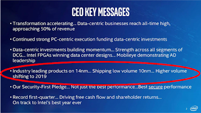
As reported by Reuters [LINK], Intel bet the earnings expectations for the first quarter driven by the biggest-ever quarterly jump in its data centre business and small-but-steady growth in its personal computer business.However, Intel also announced that they are pushing out volume production of their 10 nm Logic process to 2019, which was most recently announced for the 2nd half of 2018. during the 1Q 2018 earnings conference calls more details were given:

[Seeking Alpha, LINK] "We continue to make progress on our 10-nanometer process. We are shipping in low volume and yields are improving, but the rate of improvement is slower than we anticipated. As a result, volume production is moving from the second half of 2018 into 2019. We understand the yield issues and have defined improvements for them, but they will take time to implement and qualify. We have leadership products on the roadmap that continue to take advantage of 14-nanometer, with Whiskey Lake for clients and Cascade Lake for the data center coming later this year.

Moore's Law is essential to our strategy and our product leadership. It continues to create significant value for Intel and our customers. While it's taking longer and costing more to deliver and yield advanced process technologies, we are able to optimize our process and products within the node to deliver meaningful performance improvements.

For example, 14-nanometer process optimizations and architectural improvements have resulted in performance gains of more than 70% since the first 14-nanometer products were launched. We combine these advances in manufacturing technology and architecture to produce truly leadership products. And it's that product leadership that ultimately matters most to our customers and end users."

Brian M. Krzanich - Intel Corp.

Earnings call slides [Seeking Alpha, LINK]

In the Q&A Mr. Krzanich elaborated on the reason behind the 10 nm push out and he explained how it is mainly due to yield issues coming from multiple patterning (SADP and SAQP):

- Intel have 10 nm product and process leadership and are shipping 10 nm products today. 
- Those are the densest, highest performing products out there.
- Intel is slowing the ramp down to fix yield issues related to patterning.
- In multi-multi-patterning (SAQP) there are six layers of patterning to produce a feature. 
- Intel understand the yield issues, which are tied to 10 nm being the last technology tied to not using EUV and the amount of multi-patterning and the effects of that on defects.


Intel’s 10 nm Platform Process was presented in detail at the IEDM 2017 (Dec 2017) “A 10nm High Performance and Low-Power CMOS Technology Featuring 3rd Generation FinFET Transistors, Self-Aligned Quad Patterning, Contact over Active Gate and Cobalt Local Interconnects” and you may study the details in this excellent article by Dick James [Solid State Technology, LINK]

Media coverage:
 
The Register
 

Monday, January 22, 2018

Imec present roadmap down to 20 Ångström logic devices

From now on I think that it is time to start using Ångström instead of Nanometer (nm) when talking about leading edge CMOS and Memory.  At SEMI:s ISS 2018 (Industry Strategy Symposium) last week Luc van den Hove, Chief Executive Officer and President of Interuniversity MicroElectronics Center (IMEC) presented their roadmap for what future Logic nodes might look like going down to 2 nm that is 20 Ångström.

Key interconnect technologies named "scaling boosters" to reach down to 2 nm may be :
  • Continued scaling of self-aligned contacts
  • Cobalt "Super Via" 20 nm wide
  • Burried Ruthenium Rails only 10 nm wide, which seems to be a evolution of the tungsten burried Word Lines and Bitlines introduced by Qimonda for DRAM (65nm in 2009) except offcourse these rails are burried in a dielectric which will  make it stackable. 


Imec Logic roadmap and technologies, Picture from Twitter (LINK)


Besides the interconnect technologies the presentation showed evolution from FinFETs to nanowire FETs and Imecs latest technology development in 300 mm wafer processing technology:
  • Introduction of triple pattering (Much More ALD!)
  • EUV Litography and the introduction Carbon Nano Tube CNT Pellicle for EUV mask protection
  • Smoothening technology in patterning like Atomic Layer Etching for improving the local critical dimension uniformity (LCDU) down from 2.7 to 1.4 nm
In the case of memory technology Imec now focuses on 4 non-volatile types of memory cells besides DRAM and 3DNAND Flash:
  • STTRAM - spin transfer torque magnetoresistive random-access memory
  • RRAM - resistive random-access memory
  • FeRAM - ferroelectric random-access memory (should be renamed DD-RAM for Dresden)
  • SOTRAM - Spin Orbit Torque random-access memory


Saturday, November 25, 2017

The 7nm race by TSMC and Samsung - EUV or not EUV

According to industry sources on October 19, Samsung Electronics is considering a plan to purchase 10 extreme ultraviolet (EUV) lithography tools from the Netherlands-based ASML, the biggest semiconductor equipment maker in the world. To put tha in perspective - ASML believes that it can produce about 12 EUV lithography tools this year. It is the only company that manufactures EUV lithography tools in the world.

Sales in ALD and Etch equipment have been boosted by multiple patterning technologies based on Immersion lithography, both for Logic/Foundry and Memory. Maybe as much as 1/3 of the single/multi wafer ALD equipment market is patterning related. The last two years or so analyst have been busy trying to figure out the impact on deposition and etch equipment sales if/when EUV is introduced. Here is a recent take down by Seeking Alpha (LINK). My view is that scaling is based on symbiotic use of the latest technologies and multiple patterning and EUV will co-exist and keeping the scaling path alive. In addition, scaling opens new opportunities for ALD, ALEtch and future use of selective growth technologies with atomic scale precision. According to recent reports the ALEtch market segment is now considerd an actual segment by itself and has entered HVM (LINK).
Fudzilla reports: Korean based ETNews has mentioned that Qualcomm 7nm manufacturing has been a big win for TSMC while two other US and China customers chose Samsung’s 7nm. TSMC traditionially have dibs on Nvidia and MediaTek according to the report.

Qualcomm and Broadcom, according to the report are designing their next generation chips with TSMC’s7-nano PDK. The reason why Qualcomm went with 7nm with TSMC is the fact that the fab uses normal steppers while Samsung wants to make its 7nm with more bold and riskier EUV (Extreme Ultraviolet) photolithography technology.

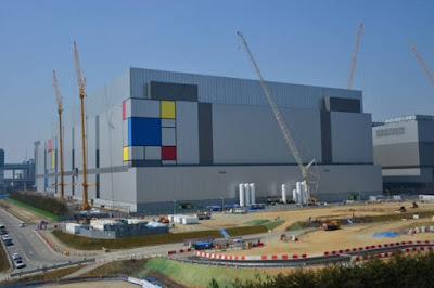
View of Samsung Electronics’ Hwasung 17 line. It is expected that Samsung Electronics will build a new 7-nano plant on a nearby site according to ETNews.

Samsung is expected to be later to the 7nm game and early adopters had to go with TSMC. EUV is still technology that is not entirely ready for the mass market and there is a disagreement weather you should need to use Extreme Ultraviolet light manufacturing with 7nm or first with 5nm. Obviously the two main fabs disagree while GlobalFoundries cooperates and shares technology with Samsung, and will have Samsung to rely upon for 7nm.

Full article: Qualcomm 7nm made by TSMC [LINK]
ETNews original source: Samsung Electronics Close to Securing Two New Customers for Its 7-Nano Foundry[LINK]
Business Korea: Keeping Leadership in 7-nano Era Samsung Electronics Seeks to Buy Up Next-gen Semiconductor Mfg Equipment

Saturday, November 19, 2016

Why is EUV so difficult and why should we ALD people care about that

Inspired by a recent article by Mark LaPedus, bad weather over Germany and coming back alive after a flue I had to return to my favorite ALD topic.  As I remember it EUV was scheduled for insertion at 32 nm and has been pushed node by node ever since then. 10 years ago when I worked at the DRAM company Qimonda (RIP) I was on a small double patterning team and at that time I got my first insights into this exciting topic and I have followed it ever since. I would say that for an ALD process engineer the HKMG stack became boring once it came into production at 45 nm. 32/28 nm let´s tune the HIG source 2 degrees Zzzzzzz. Just make up you´re mind - should we go first or last? As we care.... joking aside the three big ones, Applied Materials, Lam Research and Tokyo Electron, all failed taking control of the ALD HKMG business and this was rightfully so conquered by ASMI with a good help from Finnish and Korean ALD Technology at its finest (Microchemistry and Genitech). With respect to EUV and ALD Enabled Pattering PEALD has become a key factor and may explain partially why ASM has been successful also in that field.

Ever since ALD became part of the patterning/litho community it just feels like we are taken much more serious than when we were stuck mainly playing around with funky materials from the periodic table. In short, multiple patterning and EUV is just so much cooler! 

The situation now is that Samsung may start using EUV at 7 nm and the rest may wait until 5 nm. At least that is the current situation that I have from the last month of online media reports. That Samsung may be an early adopter for EUV maybe explained by that they have to also realize DRAM scaling sub 20 nm (more details in the article linked below).

In one sense skipping EUV has been a fantastic driver for double patterning and followed by quadruple patterning technologies realized by advanced etch processes and ALD liners. The single- and multiwafer ALD & PEALD equipment market and silicon precursor revenue volume has benefited enormously from this.

Self-aligned contact and via patterning is an established method for patterning multiple contacts or vias from a single lithographic feature. It makes use of the intersection of an enlarged feature resist mask and underlying trenches which are surrounded by a pre-patterned hardmask layer. This technique is used in DRAM cells and has been extended to patterning of active areas (see "Crossed self-aligned patterning"). It is also used for advanced logic to avoid multiple exposures of pitch-splitting contacts and vias [Wikipedia]
However, one thing that is difficult to realize with multiple patterning technology is hole patterns (described in the figure above) and here I don´t think about the regular den matrix used for e.g. DRAM cell arrays but the rather randomized pattern used for contact holes and BEOL vias. So even though you´re ALD biased at some point in time it could slow down scaling for interconnects and then that would also impact the ALD business.

So that is why it should be of interest for any ALD guy to closely follow and understand the EUV situation. Please find here some insights by Mark LaPedus at Semiconductor Engineering on what the EUV problem is all about and in great technical detail as well.

One of the most complex technologies ever developed is getting closer to rollout. Here’s why it took so long, and why it still isn’t a sure thing. November 17th, 2016 - By: Mark LaPedus, Semiconductor Engineering.

Also I can highly recommend the Wikipedia page on Multiple patterning which receives regular updates. 

To inspire you even more just take time to read this excellent review by W.M.M. Kessels et al on ALD enabled pattering: "The use of atomic layer deposition in advanced nanopatterning", Nanoscale, 2014,6, 10941-10960, DOI: 10.1039/C4NR01954G. There is definitely more to come and just maybe those holes can be made by ALD as well.


Saturday, August 13, 2016

Tokyo Electron - A spacer-on-spacer scheme for self-aligned multiple patterning and integration

Tokyo Electron showcase "A spacer-on-spacer scheme for self-aligned multiple patterning and integration" using ALD which is claimed to be a "novel, low-cost spacer-on-spacer pitch-splitting approach is targeted at sub-32nm pitch for 7nm technology nodes and beyond"

The ALD process rauns at room-temperature depositing a silicon dioxide film that is compatible with organic materials as the first spacer.

Please read the full article in SPIE News Room here.


Illustration of the proposed spacer-on-spacer SAQP integration. Depo: Deposition. Pull: Removal (of spacer). Figure form SPIE Newsroom.

Saturday, May 28, 2016

Imec Tech Forum 2016 on the future of scaling, EUV and transistor architecture

Here is a very interesting article "Event scans silicon road map, IoT as driver" by Rick Merritt in EETimes from Imec Tech Forum that took place this week in Brussels. ALD, EUV and Gate All Around Nanowire transistors is still all on the table.

As previous years Imec also this year rewarded "The imec lifetime of innovation award 2016" and this year it was given to Dr. Gordon Moore himself. Below is an interview with Gordon Moore in Hawaii made by Luc Van den Hove - President & CEO of imec.


Interview with Dr. Gordon Moore who was granted the imec lifetime of innovation award 2016. Interview by Luc Van den Hove - President & CEO of imec. [www.youtube.com]

Ivo Raaijmakers, chief technologist of equipment maker ASM International on scaling


“The industry will find a way to continue scaling, not a classic Denard scaling, but there are many innovations in the pipeline…so maybe the growth rate will decrease a bit and the cadence of new nodes will decrease…but we don’t see this as a downward spiral, just a shift from nodes maybe every three years instead of two,”

An Steegen, the senior vice president of process technology at Imec on EUV and the 5 and 3 nm nodes

“We make daily progress [on EUV]…the most complex layers at the back end where it is very difficult for immersion will be the first insertion point and the sooner the better,” said An Steegen, the senior vice president of process technology at Imec.

Rick Merritt in EETimes reports that: Steegen believes horizontal nanowires, a sort of gate-all-around deisgn, will be the next big transisitor. They could be stacked laterally to deliver 30-50% gains in lower power and higher performance, she said. Imec is still evaluating first-generation designs that it will need to prove out in second-gen hardware.

“We aways need new features to manage power density, we had dynamic frequency and voltage scaling a few years ago, FinFETs now and I believe nanowires in the future,” Steegen said.

Further out vertical nanowires could be a next step. However “going vertical is very disruptive” and these transistors cannot be stacked without area penalties, potentially forcing a move to new high-mobility III-V materials to hit performance targets, she said.

Imec is exploring lateral and vertical nanowires as successors to the FinFET. (Image: Imec) 

Full article in EETimes here.

Saturday, March 12, 2016

Great summary of the patterning options at 7nm

As many of you know, the insertion of multi patterning technology is driving the single wafer and multi wafer ALD equipment market enormously. The actually the market is predicted by many (Gartner, ASMi, VLSI) to double in the coming 2-3 years and many new players are entering ALD with new powerful ALD technology Lam Research, Applied Materials and Jusung Engineering have new platforms on the market targeting the multi patterning market and Veeco is developing new low temperature Fast Spatial ALD also targeting this market. Here is a collection of recent blog posts on this topic here at BALD Engineering ALD News Blog:

ASM International's CEO Chuck Del Prado on 2015 ALD results
Applied Materials to introduce a new system for Atomic Layer Deposition - Olympia™ ALD

Lam Research gets into the booming ALD business and doubles their install base 

Jusung Engineering launches SDP R2 Revolution-Rotation ALD System at SEMICON Korea
Veeco brings low temperature nitride Spatial FAST ALD to semiconductor manufacturing

From this point of view it is good to understand what the options are at 7nm where the number of multi patterning steps may be fore than a handful. Therefore a recommend you to read this article by Mark LaPedus in Semiconductor Engineering with the latest insights from SPIE 2016.

7nm Lithography Choices

Four possible scenarios for patterning the next generation of chips

March 7th, 2016 - By: Mark LaPedus
 
1. A chipmaker doesn’t insert EUV at 7nm, but rather it uses immersion/multi-patterning exclusively.
2. A chipmaker uses immersion/multi-patterning first. Then, EUV is inserted later in the flow where it makes sense.
3. A chipmaker inserts immersion/multi-patterning and EUV simultaneously.
4. A chipmaker uses an alternative technique, such as DSA and multi-beam.

Article:  http://semiengineering.com/7nm-lithography-choices/

Sunday, March 6, 2016

ASML and IMEC EUV Progress at SPIE Advanced Lithography Conference 2016

EUV is making progress and to several reports it may be ready for 7nm. Here you can find a report in SemiWiki by Scotten Jones on "ASML and IMEC EUV Progress" from the recent SPIE conference (21-25 February 2016, San Jose, USA). According to the report, ASML has made clear progress in throughput:
  • ASML has 8 NXE 3300 systems in the field running at ~55wph. 
  • ASML has shipped NXE3350B systems with ~125wph performance. 
  • The NXE3400B will ship this year and is expected to be the production workhorse running at ~145wph.

In another paper "Comparison of EUV and 193i based patterning for advanced node integration" Imec compared EUV to current ArFi or 193ilithography for three cases showing a cost comparasion resulting in a win for EUV : LE3 > SADP > EUV.

Abstract: "In this work we compare the pattering integrity results of product like structures using EUV- and 193i-Lithography. Traditional 193i based lithography requires multiple litho-etch (LE) or pitch doubling techniques to reach sub resolution pitch. These however add additional films and steps in the pattering process, and introduces CD and overly variability. EUV offers the possibility of single print for advanced nodes with a reduced process flow. However EUV introduces pattering selectivity and uniformity challenges. The process flows, complexity and pattering results will be presented for EUV single exposure, 193i multiple Litho Etch (LE3), and 193i Spacer Assisted Double Pattering (SADP+Keep)."

According to Scotten Jones the detailed comparison was for these 3 cases:
  1. The litho-etch-litho-etch-litho-etch (LE3) process prints 42nm lines with 144nm pitch and then shrinks them with a total of 27 steps. 
  2. The SADP process creates 48nm lines on a 96nm pitch and then shrinks them with a total of 18 steps. 
  3. EUV creates 24nm lines in an 8 step process. 
"In summary EUV had the best overall performance, SADP + block was second best and LE3 the worst. The biggest issue for EUV was LER and he thinks that can be improved." concluded Scotten Jones

Too read further about SPIE I asloo recommend this piece by Ed Korczynski at Solid State Technology looking at many additional papers presented at SPIE 2016:

http://semimd.com/blog/2016/03/03/many-mixes-to-match-litho-apps/

Wednesday, February 10, 2016

SUNY Poly in $500M EUV R&D Program with Globalfoundries, IBM and Tokyo Electron

SUNY Poly and GLOBALFOUNDRIES Announce New $500M R&D Program in Albany To Accelerate Next Generation Chip Technology. Arrival of Second Cutting Edge EUV Lithography Tool Launches New Patterning Center That Will Generate Over 100 New High Tech Jobs at SUNY Poly 


“Today’s announcement is a direct result of Governor Cuomo’s innovation driven economic development model. His strategic investments supporting the state’s world class nanotechnology infrastructure and workforce have made us uniquely suited to host the new APPC, which will enable the continuation of Moore’s Law and unlock new capabilities and opportunities for the entire semiconductor industry,” said Dr. Alain Kaloyeros, President and CEO of SUNY Polytechnic Institute. “In partnership with GLOBALFOUNDRIES, IBM and Tokyo Electron, we will leverage our combined expertise and technological capabilities to meet the critical needs of the industry and advance the introduction of this complex technology.” 

Press release from Globalfoundries: here