Tuesday, May 6, 2025
AlixLabs Secures Notice of Allowance for US Patent for Innovative Semiconductor Manufacturing Technology
Saturday, March 22, 2025
SemiWiki CEO Interview with Jonas Sundqvist of AlixLabs
In a recent interview with Daniel Nenni, Jonas Sundqvist, CEO and co-founder of AlixLabs, discussed the company’s pioneering role as the world’s only pure-play Atomic Layer Etch (ALE) equipment provider. Drawing on his academic background in ALD and CVD from Uppsala University, Sundqvist explained how AlixLabs’ APS (ALE Pitch Splitting) technology enables atomic-scale precision in semiconductor patterning. APS helps chipmakers reduce process complexity, lower costs by up to 40% per mask layer, and improve yield, particularly in advanced logic and memory manufacturing. As the industry pushes toward sub-10 nm nodes, APS offers a scalable and sustainable alternative to traditional multi-patterning and EUV lithography.
Sundqvist emphasized that AlixLabs addresses critical pain points in semiconductor production, such as increasing lithography costs, complexity, and sustainability concerns. By minimizing energy use, reducing fluorinated gas emissions, and improving process efficiency, APS supports a greener and more cost-effective manufacturing path. AlixLabs differentiates itself from giants like ASML and proponents of self-aligned multi-patterning by offering a complementary technology that simplifies patterning. The company is currently collaborating with major chipmakers and research institutes, preparing a Beta tool for pilot testing by late 2025 and targeting high-volume manufacturing between 2027 and 2029.
Sources:
CEO Interview with Jonas Sundqvist of AlixLabs - SemiWiki
EU Business Hub | Semicon Japan 2024 Business Mission - Introducing AlixLabs AB
Monday, February 10, 2025
AlixLabs Demonstrates 3 nanometers on Intel Silicon – Without EUV
The Swedish semiconductor company has fabricated leading-edge structures without using complex and costly lithography techniques.
The Swedish semiconductor company AlixLabs announces that it has used its technology to etch structures equivalent to commercial 3-nanometer circuits on Intel test silicon. Notably, this has been achieved without the use of extreme ultraviolet lithography (EUV) or advanced multi-patterning techniques such as SADP and SAQP (Self-Aligned Double Patterning and Self-Aligned Quad Patterning, respectively).
AlixLabs, a startup based in Lund, specializes in the development of Atomic Layer Etching (ALE), a type of plasma-based dry etching for cutting-edge structures, and ALE Pitch Splitting (APS), which enables transistor fins to be split using etching. The advantage of this approach is that it significantly reduces costs at the cutting edge, where wafer prices skyrocket with each new generation.
"We are pleased to demonstrate how APS can help the industry reduce its dependence on multi-patterning while lowering costs and environmental impact. Our technology enables the fabrication of sub-10-nanometer structures on silicon, and through Intel’s Test Vehicle Program, we have proven that sub-5-nanometer structures can be achieved using etching alone."– Dmitry Suyatin, CTO and Co-Founder of AlixLabs
According to Dmitry Suyatin, AlixLabs’ CTO, this demonstration was made possible through Intel’s Test Vehicle Program, which provided test silicon for AlixLabs to process with its APS technology. While ALE has traditionally been limited to structures in the 10-nanometer class, AlixLabs' APS technique has significantly simplified the manufacturing of structures smaller than 5 nanometers.
Etching 3-nanometer-class structures without advanced EUV lithography, using only immersion lithography, is a significant breakthrough—provided the technology can be scaled and applied in practical manufacturing. AlixLabs has previously stated its goal of seeing its technology adopted by TSMC and Samsung for their 2-nanometer processes.
Since the industry moved past the 28-nanometer node, multi-patterning has become increasingly necessary to create smaller structures and transistors. This lithographic technique involves breaking down complex patterns into simpler ones and sequentially patterning them onto the silicon wafer for higher precision and detail. Lithography can perform this in two, three, or four steps (SADP, SAQP), though more steps are theoretically possible, they are considered too complex and costly for practical use at smaller nodes.
"APS technology demonstrates that complex multi-patterning techniques such as SADP and SAQP are not needed to manufacture circuits at 5 nanometers and below. This increases the potential to use immersion lithography for critical mask layers in 3-nanometer processes. These results were achieved with our early Alpha equipment, and Beta equipment will follow later in 2025. We thank Intel for enabling this demonstration and providing high-quality test silicon."– Jonas Sundqvist, CEO and Co-Founder of AlixLabs
While lithographic multi-patterning is often necessary, it comes with several downsides. Each additional step requires more masks, which must be precisely aligned to form the final, complex pattern. Even a slight misalignment can lower yield and performance, but more importantly, it significantly extends production time. Avoiding multi-patterning whenever possible is therefore always preferable.
It is essential to distinguish between "nanometer-class" structures and actual physical nanometer measurements. What AlixLabs has achieved is a metal pitch (the distance between metal interconnects connecting transistor gates) of 25 nanometers through dry etching. This compares to TSMC’s most advanced 3-nanometer process, which achieves a metal pitch as low as 23 nanometers in certain high-density configurations.
AlixLabs highlights this test silicon as a major milestone towards commercialization and announces that more updates will follow later in 2025. Additional details will be presented by CTO Dmitry Suyatin at SPIE Advanced Lithography + Patterning in San Jose, California, on February 27, from 9:00–9:20 AM (local time).
Sources:
AlixLabs demonsterar 3 nanometer på Intel-kisel – utan EUV – Semi14
AlixLabs to Showcase Latest APS™ Findings at SPIE Advanced Lithography + Patterning – AlixLabs
Browse the 2025 program for SPIE Advanced Lithography + Patterning
Friday, September 13, 2024
AlixLabs Qualifies APS™ for Use In 300-millimeter Silicon Wafer Designs
AlixLabs' patented and wordmarked APS™ IP – short for Atomic Layer Etch (ALE) Pitch Splitting, here demonstrated in a simple animation.
“Proving that APS™ works on lithography designs on 300-millimeter wafers, is what we’ve all worked on since we founded AlixLabs in 2019,” says CEO and co-founder Dr. Jonas Sundqvist. “Not only do we aim to provide chip manufacturers wafer processing equipment that can create 20-nanometer half-pitch lines and critical dimension below 15 nanometers on silicon, we aim to do that at a lower cost and a more sustainable way than other technologies”
“We are also able to provide record breaking 3-nanometer critical dimension features on gallium phosphide (GaP) wafers today showing that APS™ can scale far into the future beyond what is needed today,” adds CTO and co-founder Dmitry Suyatin.
Friday, April 5, 2024
AlixLabs announces EU-wide APS Trademark and nearing commercialization on 300-millimeter wafer equipment
Saturday, January 27, 2024
AlixLabs Celebrates Gold Sponsorship at ALD/ALE 2024 in Helsinki: Honoring Dr. Tuomo Suntola and Embracing Advances in Atomic Layer Etching
We are proud to be Gold Sponsors of ALD/ALE 2024 in Helsinki, Finland . We look forward to contribute to the conference program and meet you in the exhibition. We especially look forward to join the celebration 50 Years of ALD and honor the inventor and Millennium Prize Winner 2018 Dr. Tuomo Suntola.
Saturday, February 18, 2023
ALD Stories Ep.20 - The story behind AlixLabs and ALE Pitch Splitting
Jonas Sundqvist joined the ALD Stories podcast again to talk about his company, AlixLabs! Check out their Atomic Layer Etch Pitch Splitting tech and how it challenges traditional patterning techniques.
Spotify - https://lnkd.in/djrMbZ-v
Apple - https://lnkd.in/d93sW3JK
Monday, September 26, 2022
AlixLabs proudly announce its Advisory Board
Thursday, September 15, 2022
AlixLabs AB today announced that the company has been granted a second patent in the USA relating to Atomic Layer Etch Pitch Splitting (APS) for semiconductor manufacturing
Monday, July 11, 2022
AlixLabs at AVS ALD ALE 2022 in Ghent, Belgium
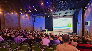
AlixLabs AB participated and presented at The AVS 22nd International Conference on Atomic Layer Deposition (ALD 2022) featuring the 9th International Atomic Layer Etching Workshop (ALE 2022) in Ghent, Belgium June 27 to 29.
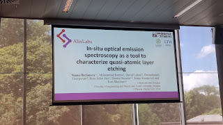
Yoana gave her oral presentation in session LE1-TuA-4 In-situ Optical Emission Spectroscopy as a Tool to Characterize Cyclic Quasi-Atomic Layer Etching, Yoana Ilarionova, Lund University, Sweden; M. Karimi, AlixLabs, Sweden; D. Lishan, D. Geerpuram, Plasma-Therm LLC, USA; R. Jafari Jam, D. Suyatin, J. Sundqvist, AlixLabs, Sweden; I. Maximov, Lund University, Sweden
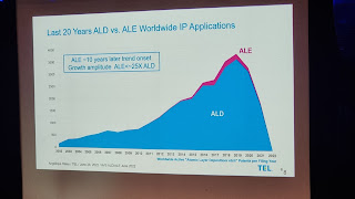
Jonas gave an invited talk for TECHCET LLC CA in: AA2-TuM2-1 High ALD Equipment and Precursor Demand and 5-Year Forecast Due to Continued Semiconductor Device Scaling and Fab Expansions.
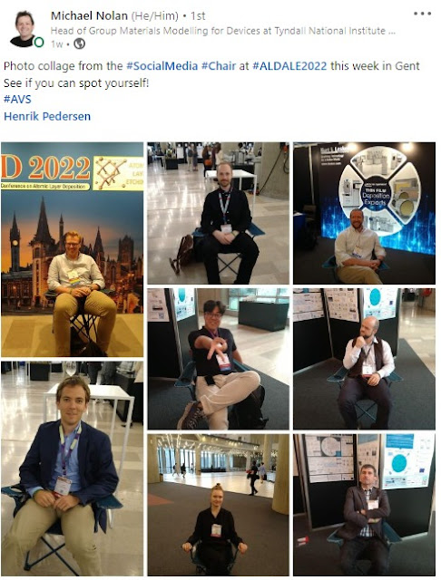
Dmitry as part of the AVS ALE Scientific Committee moderated the session ALE1-TuA In situ Studies, Mechanisms, and Modeling of ALE. We had a fantastic time and met a lot of old friends and made new ones!
Boat trip in beautiful Ghent
AVS ALD ALE 2022 Page: ald2022.avs.org/
Thursday, November 11, 2021
AlixLabs, Breaking through the Crisis – Startups
Tuesday, October 12, 2021
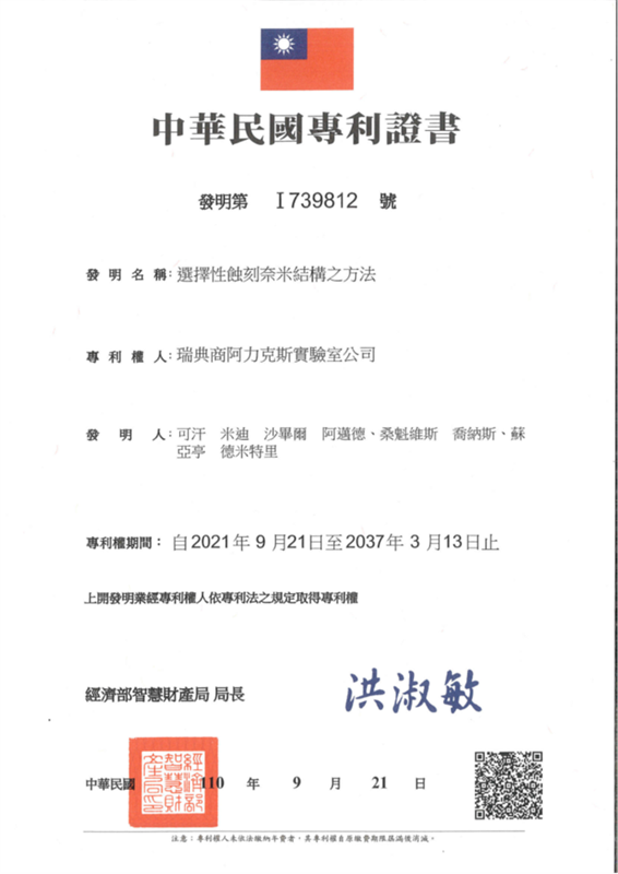
AlixLabs Granted Patent in Taiwan - The Unmatched Leader of the Global Semiconductor Industry

Saturday, October 2, 2021
Swedish Semiconductor Startup AlixLabs Raises USD 1 Million Seed Capital
Saturday, June 12, 2021
Vinova fund Swedish AlixLabs Breakthrough green technology in Nanostructures Miniaturization for Electronic Chips
Thursday, May 13, 2021
Schweden wollen mit Ätz-Spalttechnik Chipproduktion in Sachsen umkrempeln
„In Schweden haben wir keine 300-Millimeter-Infrastruktur“, erklärt „Alix Labs“-Chef Jonas Sundqvist die Kooperation mit den Sachsen. „Unsere Technologie kann in bestehende Prozessabläufe der Halbleiterherstellung integriert werden. Theoretisch könnten Chipfabriken wie die Globalfoundries-Fab 1 in Dresden unsere Methode einführen und dann 10- oder 7-Nanometer-Chips herstellen ohne teure EUV-Anlagen.“ Als Kunden sieht er aber auch Branchenriesen wie Intel, TSMC und Samsung.
Friday, April 30, 2021
The US Patent Office has approved AlixLabs’ patent application for nanofabrication by ALE Pitch Splitting (APS)
Thursday, March 18, 2021
AlixLabs AB launched ALE Pitch Splitting (APS) for the first time at ALD & ALE Ireland 2016
We did not want to steal the thunder from our good Irish friends and St. Patrick Day we wish you all a healthy recovery today and breakfast for Champions. Yesterday we remembered our trip to Dublin and launching our proprietary technology, APS - ALE Pitch Splitting, for the first time to a bigger audience. Since then a lot of things has happened at AlixLabs AB in Lund, Sweden:
- We received soft funding and invest support to found the company by LU Holding (LINK) - AlixLabs AB in Lund, Sweden operating out of IDEON Science park (LINK) and Lund Nano lab at Lund University
- We received SwedishVinnova grant for "Innovative startups" 93 startup-bolag får dela på 28 miljoner | Vinnova
- We hired our first Full-time employee Dr. Mohammad Karim, Principal Scientist (LINK)
- We signed an agreement to use the lab facilities of Sweden’s largest research environment for nanoscience and nanotechnology - Lund Nano Lab (LINK)
- We applied for an Additional 2.7 MSEK EU and National Swedish Soft co-funding in early 2021 and have additional 3 projects in the pipeline.
- We have started our 1st Investment round to close before Swedish Midsummer - please get in touch if you want a meeting! (jonas@alixlabs.com or LinkedIn: LINK)
ALE Pitch Splitting (APS) taking place at the Lund Nano Lab exhibition stand in the ALD Ireland 2016 Industry Exhibition.
Video from presentation invited given by Dr. Dmitry Suyatin LINK. Staff Engineer at Lund Nano Lab and CTO of AlixLabs AB and on the Scientific Committee of AVS ALE.