Showing posts with label ALD - Atomic Layer Deposition. Show all posts

Wednesday, September 27, 2023

Forge Nano and KULR Partner for Cutting-Edge Battery Safety & Performance

In a significant move to enhance battery safety and efficiency, KULR Technology Group, a key player in sustainable energy management, has formed a strategic partnership with Forge Nano, renowned for its precision nanocoating technology. This alliance, estimated to be worth between $3.5 million to $5 million, will amalgamate KULR ONE Design Solutions - which offers advanced battery cell screening - with Forge Nano’s Atomic Layer Deposition (ALD) coating technique.


The collaboration begins with an assessment of Forge Nano’s elite battery cells intended for space and the US Department of Defense (DoD). KULR's innovative automated cell screening will be instrumental in gauging various battery cell parameters, ensuring they adhere to stringent NASA flight specifications.

In light of the recent announcement by the U.S. Department of Energy about a second tranche of $3 billion funding for battery production and recycling, this partnership positions itself as a catalyst in setting new benchmarks in battery safety and performance. 

Forge Nano, after securing $50 million earlier this year, has been aggressively investing in augmenting its battery production capacities. While KULR, with its expansive market presence in diverse sectors, sees this collaboration as a strategic alignment towards advancing the future of energy storage.

Source: Forge Nano and KULR Form a Strategic Partnership for Enhanced Battery Safety and Performance - Forge Nano

Wednesday, September 20, 2023

Linköping University Researchers Uncover Challenges in Thermal ALD of Indium Nitride (InN)

Researchers from the Pedersen Group at Linköping University have investigated the limitations of thermal atomic layer deposition (ALD) for indium nitride (InN). Using quantum-chemical density functional theory calculations, they explored the adsorption process of ammonia (NH3) on InN and compared it to gallium nitride (GaN), shedding light on the challenges in InN deposition.

InN holds promise in semiconductor and electronics applications due to its distinctive properties. It boasts a high electron mobility, exceeding that of many other III-nitride materials, rendering it suitable for high-frequency electronic devices like transistors and amplifiers. With a narrow bandgap of around 0.7 eV, InN finds applications in infrared photodetectors and optoelectronic devices. Despite challenges in thermal stability during deposition, it exhibits good stability when appropriately processed, making it valuable in high-temperature electronics. Its high electron velocity enhances the performance of high-speed field-effect transistors. InN also shows potential in energy-efficient electronics and gas sensing applications, furthering its significance in the semiconductor and electronics industry.

The deposition of indium nitride (InN) using CVD is challenging due to its low thermal stability, which limits the use of high-temperature processes. ALD is an alternative method that can operate at lower temperatures. While ALD has been successful in depositing materials like aluminum nitride and gallium nitride (GaN) using ammonia as a nitrogen precursor in thermal processes, InN can only be deposited using plasma ALD. This suggests a limitation to thermal ALD with ammonia for InN.


Gibbs free energy profile for the adsorption of NH3 onto InN and GaN at 500 (a) and 800 K (b).

Researchers used quantum-chemical density functional theory calculations to investigate the adsorption process of ammonia (NH3) on both GaN and InN surfaces. They aimed to understand if differences in this process could explain why thermal ALD of InN is challenging. Their findings revealed a similar reactive adsorption mechanism on both materials, where NH3 adsorbs onto vacant sites created by the desorption of methyl groups from the surfaces. However, the energy barrier for this adsorption process was significantly higher on InN compared to GaN, indicating that the process is much slower on InN.

This slow kinetics would hinder NH3 from effectively adsorbing onto InN during the ALD growth process, making thermal ALD with InN using NH3 impractical. As a result, the only alternative to a fully thermal ALD process for InN appears to be using a different precursor system due to InN's thermal instability.

Source: On the limitations of thermal atomic layer deposition of InN using ammonia | Journal of Vacuum Science & Technology A | AIP Publishing

Saturday, September 9, 2023

Unlock the Future of Materials and Products: Join the MERCK ALD and ALE Innovation Webinar!

Join us for an exciting event on October 18, 2023: "Revolutionizing Materials and Products: Innovations in Atomic Layer Deposition (ALD) and Atomic Layer Etch (ALE)." Presented by Sergei Ivanov, Senior R&D Manager at Merck KGaA, and Martin McBriarty, Senior Scientist, this webinar promises groundbreaking insights into the world of materials and product innovation.

Event Details:

Date: October 18, 2023

Time: 4:00 pm - 5:00 pm CET

Host: Laith Altimime, President of SEMI Europe

Agenda:

- 4:00 pm CET - Welcome remarks by Laith Altimime, President, SEMI Europe.

- 4:05 pm CET - "Revolutionizing Materials and Products: Innovations in Atomic Layer Deposition (ALD) and Atomic Layer Etch (ALE)" by Sergei Ivanov & Martin McBriarty.

- 4:45 pm CET - Q&A session moderated by Laith Altimime, followed by conclusions from all speakers.

About the Speakers:

Sergei Ivanov: Sergei is the Senior R&D Manager in the Organometallics division of Thin Films Business. He leads a research program focused on developing novel precursors for the deposition of metal, metal nitride, and metal oxide films. Sergei holds a PhD in Inorganic Chemistry from Kurnakov Institute of Russian Academy of Sciences and a B.S. in Chemical Engineering from Mendeleev University of Chemical Technology.

Martin McBriarty: Martin is a Senior Scientist leading the development of atomic layer etch and other vapor-phase etch methods. He earned his B.S. in Materials Science & Engineering at the University of Florida and his Ph.D. in the same field at Northwestern University. Martin joined Intermolecular in 2018 after completing postdoctoral research at Pacific Northwest National Laboratory.


Tuesday, September 5, 2023

Revolutionizing Pharmaceutical Packaging and Labware: ALD Technology Enhances Material Properties

Picosun, an Applied Materials company, is proud to announce a breakthrough in enhancing the properties of packaging materials and labware using Atomic Layer Deposition (ALD) technology. ALD offers impermeable barriers and functional surfaces, revolutionizing pharmaceutical packaging and labware for the better.

Date: 12th December Time: 3:00 PM London / 10:00 AM New York

As pharmaceutical packaging evolves to accommodate biological drugs and novel packaging solutions, ALD technology steps in to provide ultra-thin, uniform, and precise material layers with atomic-level thickness and composition. This innovation caters to the demands of primary packaging materials and labware, offering impermeable barriers against leachables and ensuring biocompatibility.

Join us for an insightful webinar to explore how ALD can elevate the performance of packaging materials and labware. Stay ahead in the world of pharmaceutical and medical advancements!

Register now to secure your spot and gain valuable insights. Stay at the forefront of innovation with Picosun and ALD.


Monday, September 4, 2023

Netherlands' chip tool export controls take effect for DUV Lithography and ALD

The Netherlands has enacted new export controls on cutting-edge chipmaking technology, joining the US and Japan in regulating these crucial tools. The new move, effective from September 1, targets advanced chip manufacturing equipment used in processes like deep ultraviolet (DUV) lithography and atomic layer deposition (ALD) - an add-on to previous EUV Lithography export restrictions. 

Dutch company ASML, a global leader in chipmaking equipment, will continue shipments of some advanced machines this year, but starting January 1, it expects limited export licenses for systems bound for domestic Chinese customers. 
The Dutch government says it is a matter of the country's security. "We've taken this step on national security grounds," Liesje Schreinemacher, the minister for foreign trade and development cooperation, said of the new rules.
ASM International, a Dutch company, holds a significant position in the ALD market. Renowned for its ALD equipment, ASM International plays a vital role in semiconductor manufacturing by enabling precise and thin material layering on wafers. This technology is essential for advanced chip production, impacting various industries. Its role emphasizes the impact of export controls on crucial semiconductor processes and global technology supply chains.


The regulations, driven by national security concerns, cover tools vital for producing memory chips, processors, and sensors. Chinese chipmakers have reportedly accelerated purchases of equipment ahead of the rules taking effect. China's responses include its own export curbs and efforts to bolster domestic semiconductor capabilities. The situation reflects the evolving landscape of technology export controls and their impact on international supply chains.

Source:

Friday, September 1, 2023

Unlocking MEMS Manufacturing Excellence: Dive into ALD's Potential!

Discover the transformative power of Atomic Layer Deposition (ALD) in MEMS manufacturing! Join the SEMI and Forge Nano virtual event on October 11, 8:00 am PT, as we explore ALD's role in enhancing performance and efficiency in micro-fabrication. Delve into dynamic ALD techniques, precision film deposition, and how it fuels high-volume manufacturing. Hear from experts like Matt Wiemer of Forge Nano on tuning film properties and its application in evolving MEMS architectures. Don't miss this opportunity to assess ALD's compatibility with your MEMS processes. 

Register now at the link below and unlock new dimensions in MEMS manufacturing!


Thursday, August 31, 2023

Balancing Fundamental and Applied ALD with Stacey Bent – ALD Stories Ep. 26


In Episode 26, Professor Stacey Bent from Stanford University joins to discuss all aspects of her career, including early area selective deposition work, how her different academic appointments in chemistry and engineering have influenced the direction of her work, and how ALD can be used in energy applications. Stacey and Tyler also chat about how Stacey finds the best paths for her students, how being a professor and Vice Provost feedback to each other, and new programs she has initiated in her Vice Provost position. 

In this episode: 
00:00 Introduction 
03:45 Area Selective Work 
15:40 Chemistry & Engineering Backgrounds 
21:20 ALD for energy applications 
33:54 Stacey as an advisor 
36:19 Vice Provost position
 

Wednesday, August 30, 2023

Announcement Symposium G01 on “ALD & ALE Applications, #19” at the 244th ECS Meeting in Gothenburg, Sweden, Oct. 8-12, 2023

Announcement Symposium G01 on “ALD & ALE Applications, #19

at the 244th ECS Meeting in Gothenburg, Sweden, Oct. 8-12, 2023

See for detailed information about the 48 symposia, late manuscript submission requirements, and financial assistance: https://www.electrochem.org/244/.


Early (pre-)registration deadline is September 11, 2023.


In the ONLINE PROGRAM you can find symposium G01 on “ALD & ALE Applications, #19” which runs from Monday through Thursday Oct. 9-12 with a total of 77 presentations, incl. 1 keynote and 17 invited speakers. 


Sponsors of Symposium G01 on “ALD & ALE Applications, #19”


6K Energy Partners with Forge Nano to Revolutionize Battery Material Production

6K Energy, a trailblazer in sustainable battery material production, has joined forces with Forge Nano to introduce cutting-edge Atomic Layer Deposition (ALD) technology for commercial-scale production of NMC 811 cathodes. This collaboration aims to transform the battery industry by enhancing performance, efficiency, and cost-effectiveness.


Forge Nano, known for its precision nano-coating technology, and 6K Energy are set to redefine battery material production. By integrating Forge Nano's proprietary Atomic Armor™ surface technology into 6K Energy's process, the partnership promises unparalleled advancements.

Atomic Armor employs ALD coatings with unprecedented precision and speed. This method enhances battery materials, resulting in superior capacity, safety, charging rates, and cost-efficiency. Combining Forge Nano's Atomic Armor with 6K Energy's innovative UniMelt® materials production process is expected to yield high-performance and cost-effective battery materials.

Dr. Richard Holman, Senior VP of Battery Products at 6K Energy, emphasizes the impact of the collaboration, stating, "Leveraging Forge Nano's Atomic Armor platform provides us with a coating technology that meets the stringent specifications of our lithium-ion battery materials."

6K Energy's mission to produce domestically sourced battery materials for electric vehicles and renewable energy is greatly amplified by this collaboration. As the demand for advanced battery technologies grows, strategic partnerships like this one are poised to drive sustainable and high-performance solutions.

About 6K:

6K is a sustainability-driven company offering innovative solutions across industries. Their UniMelt® microwave plasma production system transforms materials into groundbreaking products. The company's 6,000-degree philosophy signifies both the operational temperature of UniMelt and the sun's surface temperature. 6K Energy, a division focused on domestically sourced battery materials, accelerates the transition to electric vehicles and renewable energy.

For more information, visit www.6Kinc.com.

6K Energy to Implement Forge Nano Equipment for Commercial Production of NMC 811 - Forge Nano

Monday, August 28, 2023

The Future of Nanoimprint Lithography: Exploring Possibilities and Challenges for High-Volume Production

Nanoimprint lithography (NIL) has emerged as a promising technique for the replication of intricate nano-scale features, offering higher resolution and uniformity compared to traditional photolithography methods. As semiconductor technology advances towards smaller and more complex structures, NIL holds the potential to revolutionize high-volume production processes. In this blog post, we'll delve into the current status of nanoimprint lithography and the possibilities it presents for future high-volume productions, as well as the main issues and concerns that need to be addressed.

NIL utilizes a process where a patterned mask is brought into contact with a resist-coated substrate. The resist fills the relief patterns in the mask through capillary action, creating precise nano-scale features. With a focus on simplicity and cost-effectiveness, NIL doesn't require the complex optics found in traditional photolithography, making it an attractive option for semiconductor memory applications.

Early work on combining NIL and Atomic Layer Etching by AlixLabs Founders

AlixLabs (www.alixlabs.com)  founders and Lund Nano Lab (Lund University, Sweden) collaborated 2018 to exploit Atomic Layer Etching (ALE) for improved NIL quality and resolution. ALE involved Cl2 monoatomic layer adsorption on silicon, followed by controlled Cl2-modified silicon layer removal using argon bombardment. This precision process allowed diverse nanopatterns to be etched onto silicon wafers with electron beam lithography. The treated wafers served as robust nanoimprint stamps in a thermal process, transferring features as small as 30 nm into a poly(methyl methacrylate) layer. ALE's potential for ultrahigh-resolution nanoimprint stamp fabrication advances nanofabrication techniques significantly.

Most Recent Achievements:

Recent study by TEL and Canon have demonstrated NIL's resolution capabilities of better than 10 nm, positioning the technology as a candidate for printing multiple generations of critical memory levels using a single mask. The potential to eliminate material waste by applying resist only where necessary adds to its appeal. Moreover, the simplicity and compactness of NIL equipment allow for clustered setups, enhancing productivity.

NIL Addressing Challenges in DRAM Scaling:

Dynamic Random Access Memory (DRAM) memory faces the challenge of continued scaling, with roadmap targets aiming at half pitches of 14 nm and beyond. The complexities of achieving tighter overlays, greater precision in critical dimensions, and edge placement errors demand innovative solutions. In DRAM fabrication, overlay requirements are even more stringent than in NAND Flash, with an error budget of 15-20% of the minimum half pitch.

Edge Placement Error (EPE):

EPE, the difference between intended and printed features, poses a significant challenge in modern semiconductor manufacturing. The intricacies of multiple patterning schemes and intricate device layouts contribute to EPE's complexity. Ensuring accurate placement of features is critical for maintaining device yield and performance.

The Quasi-Atomic Layer Etch (Quasi-ALE) process

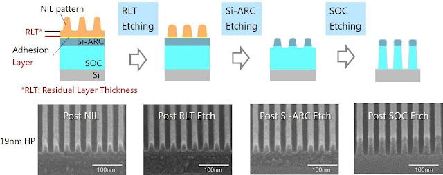
The process is a specialized etching technique employed in advanced semiconductor manufacturing, particularly in processes like Nanoimprint Lithography (NIL). Quasi-ALE combines elements of Atomic Layer Etching (ALE) and conventional etching methods to achieve precise and controlled material removal. In the context of Nanoimprint Lithography, Quasi-ALE is used to etch materials with exceptional precision, targeting nanoscale features while minimizing damage to the surrounding areas. It involves a cyclic process where alternating etching and passivation steps are applied to the substrate. Each cycle removes a controlled layer of material, ensuring highly uniform etching and minimal lateral etch. One can discribe Quasi-ALE as a more productive way of performing ALE.

The key steps of the Quasi-ALE process typically involve:

1. Etch Step: During this step, a reactive gas is introduced into the etch chamber, which chemically reacts with the material to be removed. This reaction results in the selective removal of the material layer.

2. Passivation Step: In this step, a passivating species is introduced, forming a protective layer on the substrate surface. This layer prevents further etching and preserves the material beneath.

3. Purge and Repeat: The chamber is purged to remove any excess gases, and the process is repeated in a cyclical manner. Each cycle removes a controlled atomic layer of material.

Quasi-ALE is particularly advantageous for applications requiring high precision and control, such as in Nanoimprint Lithography, where maintaining accurate pattern dimensions and minimizing damage is critical. By combining the benefits of both ALE and traditional etching, Quasi-ALE enables advanced semiconductor manufacturing processes to achieve unprecedented levels of accuracy and uniformity.


Addressing EPE with Nanoimprint Lithography:

Researchers are actively exploring techniques to mitigate edge placement errors in nanoimprint lithography. This includes focusing on overlay accuracy, critical dimension uniformity (CDU), and local CDU. Compensatory methods such as dose control and reverse tone pattern transfer are being investigated to improve CDU and minimize errors.

The Role of Dose Control:

Varying the exposure dose offers a means of achieving small shifts in critical dimensions. Initial studies suggest that dose variations could lead to CD shifts of one to 2 nm. This strategy holds promise for enhancing CDU in the imprint process.

Reverse Tone Pattern Transfer:

Reverse tone processes, involving spin-on hard mask (SOHM) application and etch-back, offer an alternative approach to pattern transfer. While this method provides advantages such as reduced resist erosion and improved wall angles, trade-offs between CDU and line width roughness (LWR) need to be addressed.

Looking Ahead: The Possibilities and Challenges:

While NIL exhibits impressive potential, there are key challenges to overcome before it can be effectively integrated into high-volume semiconductor manufacturing. Ensuring precise overlay accuracy, managing complex CDU requirements, and effectively addressing edge placement errors remain pivotal. As the industry strives to achieve the roadmap's aggressive scaling targets, the evolution of nanoimprint lithography will undoubtedly play a crucial role.

Nanoimprint lithography is poised to reshape the semiconductor manufacturing landscape, offering higher resolution and cost-efficiency compared to traditional methods. With ongoing research and development, addressing challenges such as overlay accuracy, CDU, and EPE, the path to successful high-volume production through NIL seems promising. As technology continues to advance, the journey towards perfecting nanoimprint lithography is an exciting one, holding the potential to shape the future of chip fabrication.

Tokyo Electron (TEL): 

TEL specializes in Nanoimprint Lithography (NIL) technology, offering precision equipment, advanced etching solutions, and expertise in process control. They excel in alignment, overlay correction, CDU management, and etching technology.

TEL has previously demonstrated that for sub 7  nm CMOS technology, ALE and ALD integration improves SAC and patterning processes, achieving precise CD shrinking and enhanced selectivity.

Canon: 

Canon contributes to Nanoimprint Lithography (NIL) advancement by leveraging TEL's strengths in alignment, overlay correction, CDU management, and advanced etching solutions. They integrate these capabilities with the Reverse Tone Pattern Transfer, ensuring precise pattern replication and fidelity. Canon's focus on innovation drives high-resolution, cost-effective solutions for semiconductor manufacturing.

Canon has introduced a groundbreaking solution in the field of semiconductor technology with the development of the world's first mass-production equipment called the "FPA-1200NZ2C." This innovative tool utilizes nanoimprint lithography, a cutting-edge technique that involves imprinting nanometer-scale mask patterns onto substrates. By adopting this novel approach, Canon aims to overcome the limitations of conventional miniaturization methods. The FPA-1200NZ2C is already in use by Toshiba Memory, a prominent semiconductor memory manufacturer. This advancement marks a significant step forward in semiconductor manufacturing, enabling the creation of more intricate and advanced circuit patterns.

Sources:

High-Definition Nanoimprint Stamp Fabrication by Atomic Layer Etching — Lund University

Nanoimprint post processing techniques to address edge placement error (spiedigitallibrary.org)

Nanoimprint Lithography | Canon Global

FPD Lithography Equipment | Canon Global

Benefits of atomic-level processing by quasi-ALE and ALD technique - IOPscience

www.alixlabs.com

Acknowledgement :

Thanks for sharing the SPIE article on LinkedIn and giving insights Frederick Chen!


Sunday, August 27, 2023

The Industiral Ecosystem of Si Chips and Atomic Layer Deposition - Webinar


Register now for a FREE #ACSScienceTalks #VirtualEvent with  Assoc Editor discussing "The Industrial Ecosystem of Si Chips & Atomic Layer Deposition as a Key Nanofabrication Technology." 👉brnw.ch/21wC0I4

Dutch Scientists at TNO & TU Eindhoven Develop Efficient Monolithic Perovskite-PERC Tandem Solar Cell

Highlights

  • Champion 23.7% efficient perovskite-PERC tandem cell was achieved.

  • The developed thermal atomic layer deposition (ALD) process for NiO is reported.

  • ALD NiO was added to an ITO/SAM recombination junction to improve the device yield.

Dutch researchers at TNO and TU Eindhoven have achieved a notable breakthrough in solar cell technology by creating a monolithic perovskite-PERC tandem solar cell with a remarkable 23.7% efficiency. The innovation lies in a new tunnel recombination junction (TRJ) design that includes indium tin oxide (ITO), carbazole (2PACz), and a nickel(II) oxide (NiO) layer. Unlike conventional TRJs, the addition of NiO significantly reduces electrical issues in the perovskite top cell.


(a) HAADF-scanning transmission electron microscopy (TEM) image of a tandem cell using ITO/NiO/2PACz. (b) Compositional line profiles at the interface ITO/NiO/SAM extracted from an EDX elemental mapping. Note that the figure is rotated 90°.

By using atomic layer deposition (ALD), the team improved the uniformity of the self-assembled monolayer (SAM) in the TRJ structure. This new solar cell design includes a perovskite absorber, electron transport layers, an ITO electrode, a silver (Ag) metal contact, and an antireflective coating.

Comparing their creation with a reference cell, the researchers found the novel TRJ-based cell achieved an efficiency of 23.7%, slightly below the reference cell's 24.2%. However, the novel design's uniform coverage of SAM and consistent efficiency across different devices within and between batches makes it promising for large-scale production.

Published in Solar Energy Materials and Solar Cells, this research opens doors for improved perovskite-PERC tandem solar cell technology using ALD NiO.

Atomic layer deposition of NiO applied in a monolithic perovskite/PERC tandem cell - ScienceDirect

Trelleborg Sealing Solutions Unveils State-of-the-Art Semiconductor Seals and Pioneering Engineering Expertise at Semicon Taiwan 2023: Spotlight on Atomic Layer Deposition Application

Trelleborg Sealing Solutions Exhibits Advanced Semiconductor Seals and Engineering Prowess at Semicon Taiwan 2023

Trelleborg Sealing Solutions, a leading player in engineering solutions, is making waves at Semicon Taiwan 2023 by showcasing its cutting-edge engineering capabilities and an expanded range of semiconductor sealing solutions. The event, hosted at the Taipei Nangang Exhibition Center, features Trelleborg's booth highlighting their latest additions to the Isolast PureFab FFKM material range, a significant advancement in semiconductor seal technology.

At the forefront of their display is the Isolast PureFab JPF40, an ultra-high temperature perfluoroelastomer (FFKM) designed for demanding subfab applications and thermal processes. This includes pivotal processes such as rapid thermal processing (RTP) and atomic layer deposition (ALD), crucial for semiconductor manufacturing. This material boasts unparalleled compression set performance within a wide operating temperature range, ensuring airtight seals in critical processes even at extreme temperatures reaching +300°C. The remarkable capability to withstand peak application temperatures exceeding +325°C makes it a game-changer in the semiconductor industry.

Ethan Huang, the Semiconductor Segment Manager at Trelleborg Sealing Solutions, emphasized the vital role of reliable sealing solutions in safeguarding semiconductor processes against escalating temperatures and aggressive chemical agents. The Isolast PureFab JPF40 and other offerings within the PureFab range are meticulously engineered to address the unique challenges posed by semiconductor environments.

Furthermore, Trelleborg's expertise extends to predictive engineering through finite element analysis. This innovative approach aids in modeling compression set data, allowing engineers to more accurately estimate the usable lifetime of seals during design and production. This predictive technology is a significant leap forward, enabling enhanced seal longevity assessments.

A standout in their exhibition is the Isolast K-Fab Flange Seal, designed for critical subfab applications and capable of withstanding temperatures up to +327°C, dependent on material selection. The seal's versatility in material options, including Isolast FFKM, PureFab FFKM, and PureFab Fluoroelastomer (FKM), makes it adaptable to various requirements.

An interesting focus lies on Trelleborg's contributions to atomic layer deposition (ALD). Their materials, like Isolast PureFab JPF22, exhibit remarkable chemical compatibility with wet process chemicals, steam, and amine-based ALD precursors. This makes them well-suited for ALD applications, which are vital to modern semiconductor fabrication processes.

In addition to their product lineup, Trelleborg also presents the Turcon Variseal NW, showcasing their prowess in spring-energized seals for extreme environments. This seal operates across an extensive temperature range and excels in both wear resistance and friction characteristics.

Semicon Taiwan 2023 provides a platform for Trelleborg Sealing Solutions to not only showcase their groundbreaking products but also to engage with industry professionals about their specific sealing needs. The event highlights the convergence of innovative engineering and the semiconductor industry's evolving demands.

Friday, August 25, 2023

TRION Battery and Forge Nano Partner to Advance Lithium-Ion Battery ALD Tech

TRION Battery Technologies and Forge Nano have teamed up to revolutionize lithium-ion battery performance. This strategic partnership combines Forge Nano's Atomic Layer Deposition (ALD) coating technology with TRION's innovative SX-silicon materials to enhance batteries for aerospace, defense, and other high-demand markets.

TRION Battery Technologies and Forge Nano have signed a Memorandum of Understanding (MoU) to jointly develop lithium-ion battery solutions. This collaboration marks the beginning of a journey toward improved battery performance.

Forge Nano's ALD material coatings have shown significant improvements on various battery electrode materials. The partnership aims to achieve similar breakthroughs by combining these coatings with TRION's SX-silicon materials. TRION's SX-silicon has successfully overcome challenges associated with silicon use in batteries, achieving impressive milestones.

This partnership caters to demanding markets like defense, aerospace, and electric mobility. As batteries become vital in these sectors, the collaboration promises to showcase the strengths of both technologies.

The partnership accelerates TRION's SX-silicon commercialization strategy, reinforcing its value proposition to cell manufacturers. Forge Nano sees the partnership as aligning with their target markets and aims to establish a strong US supply chain.

The MoU outlines joint testing of ALD coatings on TRION's SX-silicon. The partnership aims to extend battery life, improve energy density, and enhance overall safety and efficiency in lithium-ion batteries.

TRION Battery and Forge Nano's partnership is set to reshape lithium-ion battery technology. By combining their expertise and materials, they're on a path to enhance battery capabilities for critical industries. This collaboration demonstrates the potential of synergy in driving technological advancement


TRION Battery Technologies and Forge Nano are poised to revolutionize lithium-ion battery safety and performance through their strategic collaboration. Integrating Forge Nano's advanced Atomic Layer Deposition (ALD) technology, known as Atomic Armor®, with TRION's innovative SX-silicon materials, the partnership aims to enhance battery capabilities for aerospace, defense, and beyond. By creating protective ALD coatings on electrode surfaces, they prevent degradation, improve heat dissipation, and mitigate reactivity during thermal runaway. This innovative approach not only promises higher performance but also addresses critical safety concerns, solidifying their position as pioneers in the realm of advanced battery technology.


German Firm EMD Electronics Invests $300 Million to Expand Semiconductor Manufacturing in Pennsylvania

US-based EMD Electronics, a subsidiary of German Merck KGaA, is set to bolster its North American presence by establishing a $300 million semiconductor specialty gases manufacturing facility in Schuylkill County, Pennsylvania. This strategic move, aimed at doubling their production capacity for critical semiconductor components, is anticipated to generate 68 job opportunities.

The endeavor enjoys financial backing from the Pennsylvania Department of Community and Economic Development, underscoring the state's commitment to fostering business expansion. This expansion not only highlights the industry's focus on supply chain resilience, domestic manufacturing, and emerging technologies like semiconductors for AI, IoT, and 5G, but also emphasizes the notable German origin of the company.


Tuesday, August 22, 2023

Nanexa's Breakthrough: Lenalidomide Controlled Release Confirmed in Phase 1 Study

Nanexa AB, a pioneering pharmaceutical company, has unveiled a significant advancement in the realm of drug delivery. The company recently revealed exciting results from its Phase 1 study, designated NEX-20-01, which underscored the controlled release of lenalidomide in varying doses over a span of up to 21 days.

Atomic Layer Deposition (ALD) is a cutting-edge technique used in medical and pharmaceutical applications, particularly in the development of Nanexa's PharmaShell® technology. ALD's precision in depositing thin layers of materials plays a vital role in creating the controlled-release shell of PharmaShell®. This nanoscale engineering ensures accurate drug delivery, regulating release rates and optimizing therapeutic effects. PharmaShell® benefits from ALD's versatility, enhancing drug efficacy, minimizing side effects, and allowing tailored treatment plans. ALD's role in crafting PharmaShell® exemplifies its impact in advancing drug delivery systems, revolutionizing pharmaceutical care.


The study, conducted with great precision and care, involved nine healthy volunteers who were administered either one or two subcutaneous single injections of the innovative NEX-20A formulation. This formulation encompassed doses ranging from 15 to 35 mg of lenalidomide, with a maximum cumulative dosage of 50 mg. The outcome was nothing short of remarkable, as the observed pharmacokinetic data from the human participants correlated excellently with the projected exposure calculated from preclinical studies.

Central to the accomplishment was the remarkable release mechanism employed by Nanexa, known as PharmaShell®. This ingenious approach ensured a controlled and gradual release of the drug into the participants' bodies, creating a plasma curve that spanned an impressive 21 days. A critical observation from the study was the initial low release of the total dosage within the first day. This gradual release strategy plays a pivotal role in maintaining optimal levels of the drug in the bloodstream throughout the treatment period.

Equally encouraging was the confirmation that the total exposure of lenalidomide in the plasma—measured as the area under the curve (AUC)—escalated proportionally with the administered dose. This finding aligns with the expectations and demonstrates the efficacy of the PharmaShell® system in achieving the desired therapeutic outcomes.

Nanexa's CEO, David Westberg, expressed his enthusiasm regarding this groundbreaking achievement. "This is an important achievement for Nanexa, to once again demonstrate that we can predict the release profile of PharmaShell® in humans based on preclinical data," he shared. Westberg also revealed the company's forward-looking plans, stating, "We are now continuing to optimize the formulation and are ready to plan for the next clinical study of NEX-20 in patients. In that study, where we plan to increase the dose, we want to ensure that we will continue to minimize local reactions, and we see good results from preclinical studies on how this can be done."

Safety, of course, remains a top priority in such endeavors. Nanexa is committed to compiling comprehensive safety and tolerability data, which will be meticulously assessed following the final follow-up visits for the last dose group in October. Encouragingly, the study thus far has reported limited and transient injection site reactions, with no unexpected severe or systemic side effects. This bodes well for the continued development and progress of the NEX-20 project.

Nanexa's accomplishments in the controlled release of lenalidomide mark a significant milestone not only for the company but also for the entire field of pharmaceuticals. The ability to meticulously regulate the release profile of drugs while simultaneously minimizing undesirable side effects holds great promise for revolutionizing patient care and treatment outcomes. As Nanexa continues to pave the way with its innovative approach, the future of pharmaceuticals looks more promising than ever.

Nanexa AB - Nanexa obtains pharmacokinetic data from the NEX-20 Phase 1 study confirming controlled release of lenalidomide

ALD Reactor Evolution: Tracing Milestones from Suntola to Today's Technological Landscape


The short but impactful 50-year history of Atomic Layer Deposition (ALD) has been a subject of extensive research and documentation, particularly in recent years. Examining the technology's evolution through an equipment perspective reveals the crucial role played by innovative equipment design in shaping the ALD ecosystem we have today. This ALDeep Dive episode embarks on a journey through the evolution of ALD reactors, highlighting key milestones and developments.


Episode Highlights:

**00:00 - Intro:** An introduction to the ALD technology and its rapid development over the past 50 years.

**01:33 - Suntola’s 1st Reactor:** Delving into Tuomo Suntola's original ALD reactor and its significance in kickstarting the technology's journey.

**03:15 - Suntola’s Patented Configurations:** Exploring the patented configurations of ALD reactors, including the technological advancements they brought about.

**07:38 - The First Commercial Reactor:** Reflecting on the emergence of the first commercial ALD reactor and its role in driving the technology towards industrial applications.

**10:50 - Plasma, Please:** Examining the introduction of plasma into ALD reactors and how it enhanced film deposition processes.

**15:20 - Powder ALD Reactors:** Investigating the utilization of powder-based ALD reactors, which added a new dimension to thin film deposition.

**20:37 - Reintroduction of Spatial ALD:** Discussing the reintroduction of spatial ALD and its implications for achieving precise and uniform coatings.

**24:10 - Today’s ALD Tool Landscape:** Taking a look at the current landscape of ALD tools, showcasing the advancements and variety available today.

**25:43 - Concluding Thoughts:** Summing up the journey through ALD reactor evolution and emphasizing the integral role of equipment innovation in ALD's remarkable growth.

**Key Papers & Patents:**

- "Chemical Vapor Deposition," 2014, 20, 10-11-12, 332-344

- T. Suntola, J. Antson, International patent, FIN 52359, US 4 058 430

- T. Suntola, A. Pakkala, S. Lindfors, International patent, FIN 57975, US 4 413 022

- "Journal of Vacuum Science & Technology A," Vol.29, No.5, Sep/Oct 2011

- "Journal of Vacuum Science & Technology A" 25 (5) Sep/Oct 2007

- "Applied Physics Letters" 92, 192101 (2008)

- "Journal of Vacuum Science & Technology A" 30, 021502 (2012)


This insightful ALDeep Dive episode traces the evolutionary path of ALD reactors, acknowledging their critical contribution to the ALD technology we know today. From Suntola's pioneering work to the latest advancements, the journey reveals the interconnectedness of equipment innovation and ALD's remarkable progress.

Friday, June 30, 2023

U.S. and Netherlands Tighten Restrictions on Chipmaking Equipment Sales to China, Impacting ALD and ASM International

The United States and the Netherlands are set to impose stricter restrictions on the sale of chipmaking equipment to China, aiming to prevent the use of foreign technology for military strengthening. In their efforts to curb China's access to advanced semiconductor technology, the Dutch government plans to restrict equipment from ASML, the leading chip equipment maker in the Netherlands, while the U.S. plans to further withhold Dutch equipment from specific Chinese fabs. These measures will impact atomic layer deposition (ALD) firm ASM International as well.


Besides ASM and Lithography, ASM International and ALD is of national interest to The Netherlands. During the recent Royal State Visit of King Willem-Alexander and Queen Máxima of the Netherlands to imec, ASM, a long-standing partner of imec, was in attendance. With over 30 years of partnership, ASM has made significant investments in research and development and maintains a substantial on-site team at imec known in the industry as ASM B or ASM Belgium. During the visit, ASM had the opportunity to highlight its role in the semiconductor ecosystem of both the Netherlands and Belgium, emphasizing how this collaboration connects Europe to advanced semiconductor manufacturing activities on a global scale. (Source: ASM LinkedIn)

ASML, Europe's largest chip equipment company, dominates in lithography, a crucial step in the chip manufacturing process. The Dutch government intends to announce new regulations, including a licensing requirement, for ASML's deep ultraviolet (DUV) semiconductor equipment. ASML's more sophisticated extreme ultraviolet (EUV) lithography machines are already restricted and have never been shipped to China. The U.S. is expected to identify specific Chinese facilities, possibly including those operated by SMIC, China's largest chipmaker, in a new rule that restricts foreign equipment containing any U.S. parts. ASM International, an ALD firm, is also likely to be impacted by the new Dutch regulations.

The U.S. and Dutch measures aim to prevent China from gaining access to advanced chipmaking technology that could be used for military purposes. These actions reflect the ongoing tensions between the U.S. and China regarding national security concerns and technological competition. While the exact details and timing of the restrictions may change, the increasing limitations on chipmaking equipment sales are expected to have significant implications for the global semiconductor industry and the supply chain dynamics in the coming months.

Sources:

US, Dutch set to hit China's chipmakers with one-two punch | Daily Mail Online

State visit to Belgium – programme | News item | Royal House of the Netherlands (royal-house.nl)