Thursday, June 9, 2016

ALD functionalization with ZnO generates CNTs that possess increased risk for human exposure

Here is a study on the risks of novel nano materials and in this parrticular case ZnO ALD coated multi walled carbon annotuber (MWCNTs). The study concludes that  "Pulmonary exposure to ZnO-coated MWCNTs produces a systemic acute phase response that involves the release of Zn+2, lung epithelial growth arrest, and increased IL-6. ALD functionalization with ZnO generates MWCNTs that possess increased risk for human exposure." So basically be very careful in the lab and use gloves, lab coat, safety glaces and and a mask when handling your new smart nano materials since there is no way you can tell if what you have synthesised is a potent risk for you and your surroundings. The study is OPEN ACCESS and free to download as below.

Atomic layer deposition coating of carbon nanotubes with zinc oxide causes acute phase immune responses in human monocytes in vitro and in mice after pulmonary exposure


Erinn C. Dandley, Alexia J. Taylor, Katherine S. Duke, Mark D. Ihrie, Kelly A. Shipkowski, Gregory N. Parsons and James C. Bonner
Particle and Fibre Toxicology 201613:29, DOI: 10.1186/s12989-016-0141-9 [OPEN ACCESS]

 
Background

Atomic layer deposition (ALD) is a method for applying conformal nanoscale coatings on three-dimensional structures. We hypothesized that surface functionalization of multi-walled carbon nanotubes (MWCNTs) with polycrystalline ZnO by ALD would alter pro-inflammatory cytokine expression by human monocytes in vitro and modulate the lung and systemic immune response following oropharyngeal aspiration in mice.
 
Methods

Pristine (U-MWCNTs) were coated with alternating doses of diethyl zinc and water over increasing ALD cycles (10 to 100 ALD cycles) to yield conformal ZnO-coated MWCNTs (Z-MWCNTs). Human THP-1 monocytic cells were exposed to U-MWCNTs or Z-MWCNTs in vitro and cytokine mRNAs measured by Taqman real-time RT-PCR. Male C57BL6 mice were exposed to U- or Z-MWCNTs by oropharyngeal aspiration (OPA) and lung inflammation evaluated at one day post-exposure by histopathology, cytokine expression and differential counting of cells in bronchoalveolar lavage fluid (BALF) cells. Lung fibrosis was evaluated at 28 days. Cytokine mRNAs (IL-6, IL-1β, CXCL10, TNF-α) in lung, heart, spleen, and liver were quantified at one and 28 days. DNA synthesis in lung tissue was measured by bromodeoxyuridine (BrdU) uptake.

Results

ALD resulted in a conformal coating of MWCNTs with ZnO that increased proportionally to the number of coating cycles. Z-MWCNTs released Zn+2 ions in media and increased IL-6, IL-1β, CXCL10, and TNF-α mRNAs in THP-1 cells in vitro. Mice exposed to Z-MWCNTs by OPA had exaggerated lung inflammation and a 3-fold increase in monocytes and neutrophils in BALF compared to U-MWCNTs. Z-MWCNTs, but not U-MWCNTs, induced IL-6 and CXCL10 mRNA and protein in the lungs of mice and increased IL-6 mRNA in heart and liver. U-MWCNTs but not Z-MWCNTs stimulated airway epithelial DNA synthesis in vivo. Lung fibrosis at 28 days was not significantly different between mice treated with U-MWCNT or Z-MWCNT.

Conclusions

Pulmonary exposure to ZnO-coated MWCNTs produces a systemic acute phase response that involves the release of Zn+2, lung epithelial growth arrest, and increased IL-6. ALD functionalization with ZnO generates MWCNTs that possess increased risk for human exposure.

Wednesday, June 8, 2016

Beneq see growth in ALD services and foundry ALD production

Beneq are reporting that a growing part of their business comes from services - that is ALD coating services. Beneq calls this Thin as a Service™ a complete thin film service solution that provides you with a quick and easy way to implement a new coating solution from the first samples to full-blown production

Beneq reports in their News Blog: A growing part of Beneq’s business comes from services. Our complete thin film service concept, Thin as a Service, which we launched last year, has been received well. The customers seem to appreciate the possibility to get a quick proof of concept of new ALD applications with ALD-123 as well as the shorter time to production enabled by our Coating Services.

There seems to be a new app in the process in our Services business unit every time you ask, and they are really interesting. To give you a better understanding about the fascinating variety of ALD applications, we have added new ALD customer cases on our Applications pages:

1) Moisture barriers for flexible and organic electronics is one of the hot topics in industrial ALD and OLED encapsulation is the hottest application.

2) Another moisture barrier application we have done several versions of is protection of scintillator plates. Scintillators are typically used in the panels of digital x-ray machines for capturing the image and they require humidity barriers, which are difficult to apply because the surface of the plates is so uneven.

3) Optical coatings is another growth area for industrial ALD. The applications in this area range from decorative coatings to demanding optical filters. A great example is NIR filters inside a tube, which are in practice impossible to create without ALD.

4) Most of the projects in Beneq Development Services are the starting point on a way towards a new industrial ALD application, but the projects can also be outsourced research projects. Sometimes we just perform ALD material research for our customers.

We will be sharing more customer project examples later. If you are interested in where atomic layer deposition can be used, remember to visit our Applications pages regularly or contact us to hear all about the latest apps. There are always new updates available at your ALD App Store.

CMC Meeting October – China Supply Chain

“CMC Meeting October – China Supply Chain”


 Interested in Participating?

I. October 2016, CMCFabs 1-Day Seminar in China- Focused on the China Supply Chain
II. May 2017: 2nd Annual Critical Materials Conference in Texas
or
III. Interested in the benefits of an Associate Membership? Please Contact us at cmcinfo@TECHCET.com 


 *PRESENTATIONS FROM CMC CONFERENCE AVAILABLE for ATTENDEES/REGISTRANTS*

For login information please contact cmcinfo@TECHCET.com

Novel energy inside a microcircuit chip: VTT developed an efficient nanomaterial-based integrated energy storage

Here is a cool energy storage device from VTT in Finland using Finnish ALD technology from Beneq - a Beneq TFS-500 reactor.
As published by VTT: VTT Technical Research Centre of Finland developed an extremely efficient small-size energy storage, a micro-supercapacitor, which can be integrated directly inside a silicon microcircuit chip. The high energy and power density of the miniaturized energy storage relies on the new hybrid nanomaterial developed recently at VTT. This technology opens new possibilities for integrated mobile devices and paves the way for zero-power autonomous devices required for the future Internet of Things (IoT).

Supercapacitors resemble electrochemical batteries. However, in contrast to for example mobile phone lithium ion batteries, which utilize chemical reactions to store energy, supercapacitors store mainly electrostatic energy that is bound at the interface between liquid and solid electrodes. Similarly to batteries supercapacitors are typically discrete devices with large variety of use cases from small electronic gadgets to the large energy storages of electrical vehicles.
The energy and power density of a supercapacitor depends on the surface area and conductivity of the solid electrodes. VTT's research group has developed a hybrid nanomaterial electrode, which consists of porous silicon coated with a few nanometre thick titanium nitride layer by atomic layer deposition (ALD). This approach leads to a record large conductive surface in a small volume. Inclusion of ionic liquid in a micro channel formed in between two hybrid electrodes results in extremely small and efficient energy storage.

The new supercapacitor has excellent performance. For the first time, silicon based micro-supercapacitor competes with the leading carbon and graphene based devices in power, energy and durability.


From Graphical abstract - Conformal titanium nitride in a porous silicon matrix: A nanomaterial for in-chip supercapacitors, Nano Energy26(2016)340–345, doi:10.1016/j.nanoen.2016.04.029
Micro-supercapacitors can be integrated directly with active microelectronic devices to store electrical energy generated by different thermal, light and vibration energy harvesters and to supply the electrical energy when needed. This is important for autonomous sensor networks, wearable electronics and mobile electronics of the IoT.

VTT's research group takes the integration to the extreme by integrating the new nanomaterial micro-supercapacitor energy storage directly inside a silicon chip. The demonstrated in-chip supercapacitor technology enables storing energy of as much as 0.2 joule and impressive power generation of 2 watts on a one square centimetre silicon chip. At the same time it leaves the surface of the chip available for active integrated microcircuits and sensors.

VTT is currently seeking a party interested in commercializing the technique.

VTT's article on integrated energy storage will be published in Nano Energy magazine (Volume 26, August 2016, pages 340-345). The article can be read online: http://dx.doi.org/10.1016/j.nanoen.2016.04.029

Ultratech Cambridge Nanotech Enter Into JDP With IMEC To Study Area-Selective Deposition Technology

SAN JOSE, Calif., June 8, 2016 /PRNewswire/ -- Ultratech, Inc. (Nasdaq: UTEK), a leading supplier of lithography, laser­ processing and inspection systems used to manufacture semiconductor devices and high-brightness LEDs (HB­ LEDs), as well as atomic layer deposition (ALD) systems, announced that its Cambridge Nanotech business unit Ultratech-CNT has entered into a Joint Development Program (JDP) with IMEC in the field of Area-Selective Deposition (ASD) technology. The ASD project will concentrate on the study and use of Self-Assembled Monolayers (SAMs) as a means of functionalizing surfaces to selectively inhibit ALD-grown films. Ultratech-CNT's Savannah S300 ALD system will be used for this project to explore the use of SAMs and ALD films on 300-mm wafers using a single platform. 


Laurent Lecordier, Ph.D., senior research scientist at Ultratech-CNT, has been active in research that combines SAMs and ALD. According to Lecordier, "The broader implications of this technology suggest that we will not only be able to address the field of ASD, but we will also be able to make positive contributions in industrially-relevant areas, such as low-k pore filling, work function modifications, and surface energy tuning. With the JDP in place, I am very much looking forward to participating in this work, which has garnered strong industrial and academic interest."


Given the large potential for producing disruptive applications using the combined SAMs and ALD system, (including ASD, low-k pore filling, work function modifications, surface energy tuning, and novel materials growth), Ultratech-CNT believes this collaborative program will yield high impact results.


Savannah S300 ALD System
The Savannah family of ALD systems (S100, S200, S300) has become the preferred system for university researchers worldwide engaged in ALD and looking for an affordable yet robust platform. With a wide array of process oriented options, such as low vapor pressure precursor delivery, and plasma, along with a range of real-time analytical options such as in-situ ellipsometry, in-situ quartz crystal microbalance, and mass spectrometry -- the Savannah enables the serious researcher to deposit and study a broad spectrum of single and multi-component ALD films and Self-assembled Monolayers. With over 1000 peer-reviewed journal publications referencing its ALD systems, Ultratech-CNT's ALD instruments maintain a leading position as the tools-of-choice among active researchers.

Saturday, June 4, 2016

2nd Generation Spatial ALD from SoLayTec

The article is both in Chinese and English
Last December SoLayTec celebrated its 5th anniversary, and in the meantime has installed about twenty items of ALD equipment in the PV industry. We are happy to be the leading ALD supplier in this market. Unfortunately, while we are not yet number one in the market for Al2O3 passivation, we do expect to win further market share with our 2nd generation ALD system. As we all know, a successful product is based not only on the right timing of the market introduction but also on its uniqueness and user-friendliness. After installing machines at various PV manufacturers, we started to learn about the pros and cons of our system. In this article I would like to explore both these topics and convince you to become one of our next ALD users.
"Published PES magazine edition PES Solar China issue 2016"
- See more at: http://www.solaytec.com/publications#sthash.ni8K3irp.dpuf
Here is an article in both in Chinese and English about recent progress by SoLayTec and the 2nd generation Spatial ALD technology they are bringing to the PV ALD Al2O3 backside passivation market.

Last December SoLayTec celebrated its 5th anniversary, and in the meantime has installed about twenty items of ALD equipment in the PV industry. We are happy to be the leading ALD supplier in this market. Unfortunately, while we are not yet number one in the market for Al2O3 passivation, we do expect to win further market share with our 2nd generation ALD system. As we all know, a successful product is based not only on the right timing of the market introduction but also on its uniqueness and user-friendliness. After installing machines at various PV manufacturers, we started to learn about the pros and cons of our system. In this article I would like to explore both these topics and convince you to become one of our next ALD users.


You may have noticed that it rains a lot across Europe this early summer. Here is a picture form the other day when I test the SoLayTec spatial ALD technology.


"Published PES magazine edition PES Solar China issue 2016"

- See more at: http://www.solaytec.com/publications#sthash.ni8K3irp.dpuf

The article is both in Chinese and English
Last December SoLayTec celebrated its 5th anniversary, and in the meantime has installed about twenty items of ALD equipment in the PV industry. We are happy to be the leading ALD supplier in this market. Unfortunately, while we are not yet number one in the market for Al2O3 passivation, we do expect to win further market share with our 2nd generation ALD system. As we all know, a successful product is based not only on the right timing of the market introduction but also on its uniqueness and user-friendliness. After installing machines at various PV manufacturers, we started to learn about the pros and cons of our system. In this article I would like to explore both these topics and convince you to become one of our next ALD users.
"Published PES magazine edition PES Solar China issue 2016"
- See more at: http://www.solaytec.com/publications#sthash.cRQOwaBN.dpuf

Thursday, June 2, 2016

Speaker & Abstracts for Atomic Layer Etching 2016 Workshop in Dublin

Now the complete program for the ALE 2016 Workshop that runs in parallel to ALD2016 in Dublin has been released. Plead find the programme and links to abstract below.


Monday 25 July, Monday 25 July

Thermal ALE

10:45-12:15
Liffey Hall 1
Workshop: Thermal ALE
Chair: to be confirmed
O17 Developments in Thermal Atomic Layer Etching Using Sequential, Self-limiting Reactions
Steven George*, Younghee Lee, Jaime DuMont, Nicholas Johnson, Amy Marquardt
University of Colorado, USA
10:45-11:15
O18 Isotropic atomic layer etching of silicon nitride for 3D device applications
Kazunori Shinoda*1, Nobuya Miyoshi1, Hiroyuki Kobayashi1, Masaru Kurihara1, Tadamitsu Kanekiyo2, Masaru Izawa2, Kenji Ishikawa3, Masaru Hori3
1Hitachi, Japan, 2Hitachi High-Technologies, Japan, 3Nagoya University, Japan
11:15-11:45
O19 Low-Temperature Selective Tungsten Hexafluoride Chemical Vapor Etching of TiO2 Films
Paul Lemaire*, Gregory Parsons
North Carolina State University, USA
11:45-12:00
O20 A two-step atomic layer etching process on MoS2 realized by remote O2 plasma
Hui Zhu, Xiaoye Qin, Lanxia Cheng, ANgelica Azcatl, Jiyoung Kim, Robert Wallace*
University of Texas at Dallas, USA
12:00-12:15


Non-traditional ALE approaches

13:45-15:15
Liffey Hall 1
Workshop: Non-traditional ALE approaches
Chair: to be confirmed
O32 Longitudinal nanowire splitting by atomic layer etching
DMITRY B. SUYATIN*, MD SABBIR AHMED KHAN, JONAS SUNDQVIST, ANDERS KVENNEFORS, MARIUSZ GRACZYK, NICKLAS NILSSON, IVAN MAXIMOV
Lund University, Sweden
13:45-14:00
O33 A novel atomic layer etching of SiO2 with alternating O2 plasma with fluorocarbon film deposition
Takayoshi Tsutsumi*1, Masaru Zaitsu2, Akiko Kobayashi2, Hiroki Kondo1, Toshihisa Nozawa2, Nobuyoshi Kobayashi2, Masaru Hori1
1Nagoya University, Japan, 2ASM Japan K. K., Japan
14:00-14:15
O34 Towards wet-chemical atomic layer etching of III-V and Ge for N7 and N5 technology nodes
Dennis H. van Dorp*, Sophia Arnauts, David Weinberger, Farid Sebaai, Niamh Waldron, Frank Holsteyns
Imec, Belgium
14:15-14:45
O35 Accelerated Neutral Atom Beam Procssing for Atomic Level Etch
Craig Huffman*1, Francis Goodwin1, Satyavolu Papa Rao1, Brendan O'Brien1, Edward Barth1,4, Saikumar Vivekanand3, Martin Rodgers3, Sean Kirkpatrick2, Michael Walsh2,4, Richard Svrluga2,4
1SUNYPoly SEMATECH, USA, 2Exogenisis Corporation, USA, 3CNSE SUNYPoly, USA, 4Neutral Physics Corporation, USA
14:45-15:00
O36 InGaAs Atomic Layer Etching
Jinwoo Park*, Geunyoung Yeom
Sungkyunkwan University, Republic of Korea
15:00-15:15


Advances in applications and hardware of ALE

15:45-17:15
Liffey Hall 1
Workshop: Advances in applications and hardware of ALE
Chair: to be confirmed
O48 Plasma source configuration impact on surface processes for high precision etch
Akira Koshiishi*1, Alok Ranjan2, Peter Ventzek3
1Tokyo Electron Miyagi Ltd., Japan, 2TEL Technology Center, America, LLC, USA, 3Tokyo Electron America, Inc., USA
15:45-16:15
O49 Electron Beam Generated Plasmas: An ultra low Te route toward ALEt
David Boris*, George Petrov, Tzvetelina Petrova, Scott Walton
U.S. Naval Research Laboratory, USA
16:15-16:30
O50 Investigating the role of neutral transport in ALE and RIE processes using a 3-dimensional Monte Carlo Feature Profile Model
Chad M. Huard*1, Mark J. Kushner1, Yiting Zhang2, Saravanapriyan Sriraman2, Alex Paterson2
1University of Michigan, USA, 2Lam Research Corp., USA
16:30-16:45
O51 Atomic layer processing by conventional and low electron temperature plasma sources: a feasibility study
Hiroyuki Miyazoe*1, Ashish Jagtiani1, Josephine Chang1, Demon Farmer1, Michael Engel1, Deborah Neumayer1, Shu-Jen Han1, Sebastian Engelmann1, David Boris2, Sandora Hernández2, Evgeniya Lock2, Scott Walton2, Eric Joseph0
1IBM TJ Watson Research Center, USA, 2Naval Research Laboratory, USA
16:45-17:00
O52 Atomic Layer Etching of Silicon Nitride using Hydrofluorocarbon Chemistry
Yohei Ishii*, Kazumasa Okuma, Tiffany Saldana, Nobuyuki Negishi, Jim Manos
Hitachi High Technologies America, Inc., USA
17:00-17:15


ALD Lab Saxony at ALD2016

ALD Lab Saxony presenting oral presentations at ALD2016


Wege, Stephan
plasway-Technologies GmbH, Germany
Plasma Processing Reactor Design
Sunday 24 July: Tutorial: Plasma processing - Sunday 24 July 14:15-15:45
14:45-15:15

Hossbach, Christoph
TU Dresden, Institute of Semiconductors and Microsystems, Germany
Organic electronic devices with inorganic high-k gate oxides grown by Atomic Layer Deposition
Tuesday 26 July: High-k dielectrics 1 - Tuesday 26 July 08:45-10:15
09:15-09:30

Junige, Marcel
Technische Universität Dresden, Germany
The ALD of Ru and RuO2 – An intertwined special case
Wednesday 27 JULY: Noble metals - Wednesday 27 July 08:15-10:15
09:15-09:30

Knaut, Martin
Technische Universtität Dresden, Institute of Semiconductors and Microsystems, Germany
Atomic layer deposition and 3D nanoscale substrates - nanowires, nanotubes and nanopores
Wednesday 27 JULY: High aspect ratio nanostructures - Wednesday 27 July 16:00-17:30
16:00-16:15

Wednesday, June 1, 2016

Solar cells of the future could be based on iron molecules

Researchers at Lund University - NanoLund - have successfully explained how iron-based dyes work on a molecular level in solar cells. The new findings will accelerate the development of inexpensive and environmentally friendly solar cells.
 
 
The goal is to be able to use iron-based dyes in solar cells in the future. By using iron instead of other more expensive and rare metals, the production of solar cells and light catchers will become cheaper and more environmentally friendly. The demand for solar cells is therefore expected to significantly increase.


“In this new study, we explain how iron-based dyes work on a molecular level. That way we are able to further improve these iron complexes so that they become even better at absorbing and storing solar energy”, says senior lecturer Petter Persson.

ALD2016 Speakers and Conference Programme announced!

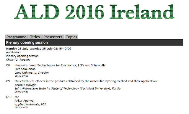
The conference programme for the The 16th International Conference on Atomic Layer Deposition, Dublin Ireland can now be viewed here.

Conference Timings:

Sunday 24 July:

Tutorial runs 13:00-17:00 in Convention Centre. Welcome reception that evening in Guinness Storehouse.

Monday 25 July – Wednesday 27 July:


ALD2016 Conference will open at 8:15 in Convention Centre and closes at 17:45 on Wednesday 27 July followed by a gala dinner on Wednesday evening.

Opening plenary invited talk by Prof. Lars Samuelson, NanoLund, Lund University Sweden followed by Prof. Anatolii Malygin, Saint-Petersburg State Institute of Technology, Russia and Ankur Agarwal, Applied Materials, USA.

ALD 2016 Conference Logo
The 16th International Conference on Atomic Layer Deposition (ALD 2016) will be a three-day meeting dedicated to the science and technology of atomic layer controlled deposition of thin films. In every year since 2001, the conference has been held alternately in United States, Europe and Asia, allowing fruitful exchange of ideas, know-how and practices between scientists. This year, the ALD conference will incorporate the Atomic Layer Etching 2016 Workshop, so that delegates at the two events can interact freely. The conference will take place on 24-27 July 2016 at the Convention Centre Dublin, Ireland.

Atomic Layer Deposition (ALD) is used to fabricate ultrathin and conformal thin film structures for many semiconductor and thin film device applications. A unique attribute of ALD is that it uses sequential self-limiting surface chemistry to achieve control of film growth in the monolayer or sub-monolayer thickness regime. ALD is receiving attention for its applications in leading-edge electronic technologies, advanced microsystems, displays, energy capture and storage, solid state lighting, biotechnologies and medical technologies. Indeed ALD is particularly advantageous for any advanced technology that requires control of film structure in the nanometer or sub-nanometer scale.

As in past conferences, the meeting will be preceded by one day of tutorials. An industry trade show will be held in conjunction with the conference, to act as common ground for academia and industry to meet and discuss the future applications of ALD. Extra opportunities for collaboration will be provided through working groups of the COST Action ‘Hooking together European research in atomic layer deposition (HERALD)’.

This conference offers an excellent opportunity to learn about the most recent R&D activities in ALD science and technology from researchers around the world. We look forward to your participation.

ALD 2016 Co-Chairs:
Simon Elliott, Tyndall National Institute , Ireland Jonas Sundqvist, Division of Solid State Physics, Lund University, Sweden
Simon Elliott
Tyndall National Institute,
Ireland
Jonas Sundqvist
Division of Solid State Physics,
Lund University, Sweden

The BALD ALD News Blog visitor statistics May 2016


Please visit here for Sponsoring!


Directing Matter: Toward Atomic-Scale 3D Nanofabrication

Here is a new review article on atomic scale 3D nanofabrication by researchers at Oak Ridge National Laboratory. You can find a full review of the article by Michael Berger in Nanowerk here.

Directing Matter: Toward Atomic-Scale 3D Nanofabrication

Stephen Jesse, Albina Y. Borisevich, Jason D. Fowlkes, Andrew R. Lupini, Philip D. Rack, Raymond R. Unocic, Bobby G. Sumpter, Sergei V. Kalinin, Alex Belianinov, and Olga S. Ovchinnikova
ACS Nano, Article ASAP
DOI: 10.1021/acsnano.6b02489
Publication Date (Web): May 16, 2016


Enabling memristive, neuromorphic, and quantum-based computing as well as efficient mainstream energy storage and conversion technologies requires the next generation of materials customized at the atomic scale. This requires full control of atomic arrangement and bonding in three dimensions. The last two decades witnessed substantial industrial, academic, and government research efforts directed toward this goal through various lithographies and scanning-probe-based methods. These technologies emphasize 2D surface structures, with some limited 3D capability. Recently, a range of focused electron- and ion-based methods have demonstrated compelling alternative pathways to achieving atomically precise manufacturing of 3D structures in solids, liquids, and at interfaces. Electron and ion microscopies offer a platform that can simultaneously observe dynamic and static structures at the nano- and atomic scales and also induce structural rearrangements and chemical transformation. The addition of predictive modeling or rapid image analytics and feedback enables guiding these in a controlled manner. Here, we review the recent results that used focused electron and ion beams to create free-standing nanoscale 3D structures, radiolysis, and the fabrication potential with liquid precursors, epitaxial crystallization of amorphous oxides with atomic layer precision, as well as visualization and control of individual dopant motion within a 3D crystal lattice. These works lay the foundation for approaches to directing nanoscale level architectures and offer a potential roadmap to full 3D atomic control in materials. In this paper, we lay out the gaps that currently constrain the processing range of these platforms, reflect on indirect requirements, such as the integration of large-scale data analysis with theory, and discuss future prospects of these technologies.

Tuesday, May 31, 2016

VPHA voting open DL Jun 15 - "conclusive reading list of early ALD publications"

VPHA voting open DL Jun 15 - "conclusive reading list of early ALD publications"

Voting is now open to determine the conclusive recommended reading list of early ALD publications, as promised in the abstract of poster presentation of the Virtual Project on the History of ALD (VPHA) at the ALD 2016 Ireland conference.
 
Please check out the details in Riikka´s ALD History Blog : http://aldhistory.blogspot.de/2016/05/vpha-voting-open-dl-jun15.html

RASIRC Presents Novel Source for Oxidation and Nitridation for Atomic Layer Deposition

RASIRC Presents Novel Source for Oxidation and Nitridation for Atomic Layer Deposition
Describes anhydrous hydrazine and hydrogen peroxide surface functionalization and passivation

San Diego, Calif – May 31, 2016 –RASIRC today announced that Chief Technology Officer Dan Alvarez, PhD will present today Novel Oxidants and Sources of Nitrogen for Atomic Layer Deposition at the 229th Electrochemical Society Conference. The conference, held May 29-June 2, 2016 in San Diego, California, is a forum for sharing the latest scientific and technical developments in electrochemistry and solid state science and technology.
The RASIRC presentation describes how development of novel metal precursors for atomic layer deposition (ALD) has been driven by the need for improved high-K materials and low temperature deposition for metal nitride films. These metal precursors in turn require novel oxidant and nitrogen sources that are more reactive than water and ammonia but less aggressive than ozone and plasma methods. Alvarez will present data on how anhydrous hydrogen peroxide and anhydrous hydrazine have shown feasibility in ALD.

“The challenge for using anhydrous hydrogen peroxide and anhydrous hydrazine in commercial application has been that they are both difficult to deliver safely in a consistent and stable concentration,” said Alvarez. “RASIRC has developed and tested a method that overcomes these problems, making it practical for industry to use these reactive chemicals with new materials in ALD.”

The RASIRC formulation for delivery of highly reactive chemicals uses an inert organic solvent and membrane delivery system that delivers anhydrous gas from liquid sources. This maintains precursor vapor pressure at levels viable for ALD and raises the solution flash point, reducing risk of explosion. The RASIRC presentation will share results from experiments focused on SiGe(110) surface nucleation by anhydrous hydrogen peroxide

Saturday, May 28, 2016

Imec Tech Forum 2016 on the future of scaling, EUV and transistor architecture

Here is a very interesting article "Event scans silicon road map, IoT as driver" by Rick Merritt in EETimes from Imec Tech Forum that took place this week in Brussels. ALD, EUV and Gate All Around Nanowire transistors is still all on the table.

As previous years Imec also this year rewarded "The imec lifetime of innovation award 2016" and this year it was given to Dr. Gordon Moore himself. Below is an interview with Gordon Moore in Hawaii made by Luc Van den Hove - President & CEO of imec.


Interview with Dr. Gordon Moore who was granted the imec lifetime of innovation award 2016. Interview by Luc Van den Hove - President & CEO of imec. [www.youtube.com]

Ivo Raaijmakers, chief technologist of equipment maker ASM International on scaling


“The industry will find a way to continue scaling, not a classic Denard scaling, but there are many innovations in the pipeline…so maybe the growth rate will decrease a bit and the cadence of new nodes will decrease…but we don’t see this as a downward spiral, just a shift from nodes maybe every three years instead of two,”

An Steegen, the senior vice president of process technology at Imec on EUV and the 5 and 3 nm nodes

“We make daily progress [on EUV]…the most complex layers at the back end where it is very difficult for immersion will be the first insertion point and the sooner the better,” said An Steegen, the senior vice president of process technology at Imec.

Rick Merritt in EETimes reports that: Steegen believes horizontal nanowires, a sort of gate-all-around deisgn, will be the next big transisitor. They could be stacked laterally to deliver 30-50% gains in lower power and higher performance, she said. Imec is still evaluating first-generation designs that it will need to prove out in second-gen hardware.

“We aways need new features to manage power density, we had dynamic frequency and voltage scaling a few years ago, FinFETs now and I believe nanowires in the future,” Steegen said.

Further out vertical nanowires could be a next step. However “going vertical is very disruptive” and these transistors cannot be stacked without area penalties, potentially forcing a move to new high-mobility III-V materials to hit performance targets, she said.

Imec is exploring lateral and vertical nanowires as successors to the FinFET. (Image: Imec) 

Full article in EETimes here.

HERALD Training School on Atomic Layer Deposition 2-4 July 2016 July 2016, at Thessaloniki, Greece.

HERALD COST Action & the ISSON16 co-organize a Training School on Atomic Layer Deposition on 2-4 July 2016 July 2016, at Thessaloniki, Greece.
 
 
Six (6) students will be granted by HERALD COST Action with 650 € to participate to the lectures of the ALD Training School and ISSON16. E-mail your application to Dr. Spyros Kassavetis (skasa@physics.auth.gr). The program will be announced soon.

Deadline for applications: 5th of June 2016 .

The granted students can submit abstract and participate to NANOTEXNOLOGY 2016 Conferences under a special registration fee. The deadline for abstract submission is 5th of June 2015. For more information, you can visit our NANOTEXNOLOGY 2016 website. 


Thursday, May 26, 2016

ALD History Blog: Photos from HERALD WG2 / ALDCoE Helsinki workshop

ALD History Blog: Photos from HERALD WG2 / ALDCoE Helsinki workshop: We had a very fine HERALD/ALDCoE workshop in Helsinki early this week. About ninety people were present from four continents.


Riikka Puurunen pitching the VPHA organizational poster. Photo by Oili Ylivaara (Twitter via @rlpuu

Excellent invited talks were delivered e.g. by:
  • Prof. Marc Heyns, IMEC, Belgium, 
  • Dr. Simon Rushworth, EpiValence, UK
  • Dr. Paul Williams, Pegasus Chemicals, UK
  • Dr. David C. Smith, LAM Research, USA 
  • Prof. Christophe Detavernier, Ghent University, Belgium
  • Prof. Anjana Devi, Ruhr University Bochum, Germany
  • Prof. Jaan Aarik,  University of Tartu, Estonia
  • Prof. Erwin Kessels, Eindhoven University of Technology, The Netherlands

Picosun extends life time for flexible electronics with ALD encapsulation

ESPOO, Finland, 26th May, 2016 – Picosun Oy, the leading supplier of high quality ALD (Atomic Layer Deposition) production solutions, brings to the printed electronics market ALD equipment specifically designed for large area flexible electronics encapsulation.


Manufacturing electronic components on flexible plastic substrates enables light-weight, bendable, and lower cost end-user products. Flexible displays, wearable electronics and “smart” clothes are some of the most common examples. More specific applications can be found in medical and security industries, where advanced X-ray detectors are being developed utilizing organic electronic components printed on plastic foils.

Organic electronics has the potential to enable a whole new generation of products, but one of its main drawbacks is the components’ sensitivity to moisture and airborne impurities. Ultra-thin ALD nanolaminates provide an ideal solution to this. Flexible, invisible, and practically weightless ALD films form dense and pinhole-free encapsulation over the components’ surface, down to the smallest nanoscale details. In Picosun’s new large area ALD tools, especially developed for the needs of the printed electronics industries, high quality ALD films can be manufactured cost-efficiently on large plastic sheets and at temperatures low enough for sensitive organic materials.

“We have again put our extensive expertise in ALD system design to work to realize completely novel technology for the vast market of printed electronics. Our new, large area batch ALD systems are developed and optimized in collaboration with these industries. Their disruptive design enables cost-efficient encapsulation of large sheets of organic electronic components, producing sustainable, long-lived end products for consumers as well as industries,” summarizes Mr. Timo Malinen, Chief Operating Officer of Picosun.

Wednesday, May 25, 2016

Photoelectric Conversion by ALD TiO2/NiO p–n Junctions with Au Nanoparticles

AZONano reports: Scientists from Hokkaido University are currently analyzing the development of solar cells made of solid materials in order to enhance their ability to survive in harsh environmental conditions.


A solid-state solar cell composed of titanium dioxide, nickel oxide, and gold nanoparticles. Gold nanoparticles harvest light and provide a visible light response to the cell. Copyright: Tomoya OSHIKIRI, Hokkaido University


Properties of Plasmon-Induced Photoelectric Conversion on a TiO2/NiO p–n Junction with Au Nanoparticles

Keisuke Nakamura, Tomoya Oshikiri, Kosei Ueno, Yongming Wang, Yoshiomi Kamata, Yuki Kotake, and Hiroaki Misawa
†Research Institute for Electronic Science and ‡Creative Research Institution, Hokkaido University, N21, W10, CRIS Building, Kita-ku, Sapporo 001-0021, Japan
§ Department of Applied Chemistry & Institute of Molecular Science, National Chiao Tung University, 1001 Ta Hsueh R., Hsinchu 30010, Taiwan
J. Phys. Chem. Lett., 2016, 7 (6), pp 1004–1009
DOI: 10.1021/acs.jpclett.6b00291

Abstract

Abstract Image


We have successfully fabricated all-solid-state plasmonic photoelectric conversion devices composed of titanium dioxide (TiO2)/nickel oxide (NiO) p–n junctions with gold nanoparticles (Au-NPs) as prototype devices for a plasmonic solar cell. The characteristics of the crystal structures and the photoelectric properties of the all-solid-state devices were demonstrated. We observed that the crystalline structure of the NiO thin film and the interfacial structure of TiO2/Au-NPs/NiO changed significantly during an annealing treatment. Furthermore, the photoelectric conversion devices exhibited plasmon-induced photocurrent generation in the visible-wavelength region. The photocurrent may result from plasmon-induced charge separation. The photoelectric conversion properties via plasmon-induced charge separation were strongly correlated with the morphology of the TiO2/Au-NPs/NiO interface. The long-term stability of the plasmonic photoelectric conversion device was found to be very high because a stable photocurrent was observed even after irradiation for 3 days.

In situ metrology to characterize water vapor delivery during ALD [Open Source]

In situ metrology to characterize water vapor delivery during atomic layer deposition

Tariq Ahmido, William A. Kimes, Brent A. Sperling, Joseph T. Hodges and James E. Maslar
J. Vac. Sci. Technol. A 34, 031512 (2016) | Read More


Water is often employed as the oxygen source in metal oxide atomic layer deposition(ALD) processes. It has been reported that variations in the amount of water delivered during metal oxide ALD can impact the oxide film properties. Hence, one contribution to optimizing metal oxide ALD processes would be to identify methods to better control water dose. The development of rapid, quantitative techniques for in situwater vapormeasurements during ALD processes would be beneficial to achieve this goal. In this report, the performance of an in situ tunable diode laser absorption spectroscopy (TDLAS) scheme for performing rapid, quantitative water partial pressure measurements in a representative quarter-inch ALD delivery line is described. This implementation of TDLAS, which utilizes a near-infrared distributed-feedback diode laser and wavelength modulation spectroscopy, provides measurements of water partial pressure on a timescale comparable to or shorter than the timescale of the gas dynamics in typical ALD systems. Depending on the degree of signal averaging, this TDLAS system was capable of measuring the water partial pressure with a detection limit in the range of ∼0.80 to ∼0.08 Pa. The utility of this TDLAS scheme was demonstrated by using it to identify characteristics of a representative water delivery system that otherwise would have been difficult to predict. Those characteristics include (1) the magnitude and time dependence of the pressure transient that can occur during water injection, and (2) the dependence of the steady-state water partial pressure on the carrier gas flow rate and the setting of the water ampoule flow restriction.

JVSTA Special issue on ALD & ALE Coming up!


Special Issues

Atomic Layer Deposition - Atomic Layer Etching


JVST A is Soliciting Research Articles for Publication in a Special January/February 2017 Issue on Atomic Layer Deposition and Atomic Layer Etching
Submission Deadline:  September  6, 2016
These special issues are planned in collaboration with  ALD 2016 Conference and the ALE Workshop being held in Dublin, Ireland, during July 24- 27,  2016. The Special Issues will be dedicated to the science and technology of atomic layer controlled deposition of thin films. While a significant fraction of the articles expected are to be based on material presented at ALD 2016 and the ALE Workshop, research articles that are on ALD and ALE but not presented at this conference are also welcome: the special issue will be open to all articles on the science and technology of ALD and ALE.

Tuesday, May 24, 2016

Abstract Poster Printing for ALD2016 in Dublin

Thank you to all that have submitted abstracts. Details regarding the format for printing can be found here: Poster Printing Instructions for ALD2016. Please note that all authors are required to print their own posters and the document includes details of a local company that is located close to the Convention Centre. 

Conference Registration: Please note if you haven’t already registered place/s for the conference and this must be completed separately here.

China to enter Leading Edge ALD Market by Aixtron take over

Most focus on the reporting for the current Aixtron situation is typically focusing on MOCVD and LED business. However, I find it naturally much more interesesting in the sense of China taking over the ex-Genus ALD business unit based in Sunnyvale (USA). Aixtron is currently on the ALD Top 10 OEM ranking for ALD (Number 7 possibly) and this is a booming market because of multi patterning coming strong now and in the following nodes. Aixtron has a multi wafer ALD plattform that can most probably be used for multi patterning as well so this to me much more interesting potential than their LED business. In addition, Aixtron has had recent success on the Korean DRAM market. So just imagine the new situation if the next grand chip investment will be an etch company.


AIXTRON SE (FSE: AIXA; NASDAQ: AIXG) (“AIXTRON”) and Grand Chip Investment GmbH (“Grand Chip Investment”), a 100% indirect subsidiary of Fujian Grand Chip Investment Fund LP (“FGC”), have today entered into an agreement to take over AIXTRON. Fujian Grand Chip Investment Fund LP is a Chinese investment fund; 51% of which is held by the Chinese business man Zhendong Liu and 49% by Xiamen Bohao Investment Ltd.

Pursuant to the agreement, Grand Chip Investment has today announced its decision to launch a voluntary public takeover offer to acquire all of the outstanding ordinary shares of AIXTRON SE, including all ordinary shares represented by AIXTRON ADS. Under the terms of the agreement, AIXTRON shareholders will be offered 6.00 Euros in cash per each ordinary share. The transaction values AIXTRON’s equity, including net cash, at approximately 670 million Euros and reflects a 50.7% premium to the three-month volume weighted average share price prior to announcement. The offer shall be subject to certain closing conditions, including regulatory approvals and a minimum acceptance threshold of 60% of all of AIXTRON’s outstanding shares.

The agreement sets out the purpose and the principal terms of the transaction with FGC and the future strategy. FGC intends to support AIXTRON’s strategy going forward. R&D competency and AIXTRON’s existing technology shall be maintained at the existing technology centers. FGC has also agreed that AIXTRON shall further strengthen its technology and IP Portfolio, which shall remain vested with AIXTRON, including in Germany. AIXTRON’s existing global set up will be maintained and expanded with AIXTRON’s three technology hubs in Herzogenrath (Germany), Cambridge (UK) and Sunnyvale (USA). Further international technology hubs may be established. AIXTRON’s legal domicile and headquarters shall remain in Herzogenrath, Germany.

In the event the takeover is successful, Martin Goetzeler is to remain CEO of AIXTRON and Dr. Bernd Schulte is to remain in his function as COO. Following a successful closing of the transaction it is anticipated that Grand Chip Investment will nominate four candidates to the six-member Supervisory Board.

The University of Twente’s MESA+ institute has purchased an advanced PLD machine from Solmates

The University of Twente’s MESA+ research institute has purchased an advanced Pulsed Laser Deposition (PLD) machine from its research partner, the spin-off company Solmates. This device opens the door to the creation of new materials and chips (or individual chip components), which are constructed as a series of layers, each just one atom thick. The new machine will enable MESA+ to further strengthen its position relative to industry. This is because MESA+ NanoLab’s numerous researchers and external users will, from now on, be able to work on an industrial scale. As a result, new scientific knowledge in the areas of unconventional electronics and advanced materials will be more accessible, as well as more suitable for practical application at an earlier stage.


MESA+, the University of Twente’s nanotechnology research institute, is a leader in the creation of extremely thin layers consisting of just a single layer of atoms. This involves using a laser to transform a material into a plasma, which then condenses on a surface to form an extremely thin layer. By layering multiple very thin layers, one over the other, it is possible to create completely new chips (or individual chip components) and materials with properties that have never been seen before. The technique involved – which was partly developed at the University of Twente – is known as Pulsed Laser Deposition (PLD). Arjen Janssens, CEO of Solmates, expects that by around 2020 PLD will have evolved into one of the standard chip production systems.

Saturday, May 21, 2016

Presentations from NCCAVS Meeting on Advanced Memory availaable for Download


Recently (April 21, 2016) The North California Chapter of The American Vacuum Society (NCCAVS) Thin Film User Group organized a meeting on Advanced Memory in San Jose, California. Now all the presentations by Intel, Globalfoundries and Avalanche Technology are now available for download at the TFUG Proceedings page

The Thin Film Users Group (TFUG) focuses on state-of-art thin-films deposition and applications for semiconductor and related fields, such as nanotechnology, renewable energy, imaging devices, design for manufacturing, and advanced memory research. It is composed of engineers and scientists from device manufactures, semiconductor equipment venders and universities. The TFUG's main activity is a bi-monthly half-day open seminar from researchers and industry technologists with technical presentations on topics of current interests.
 
This event was chaired by Chakku Gopalan (Intel Corporation), Co-chared by Chari Perera (Applied Materials Deposition Products Group), Paul Werbaneth (Intevac, Inc.) and Michael Oye (UCSC).

NAND Flash: Where are we, where are we going?

Pranav Kalavade, Principle Engineer at Intel, Non-volatile Memory Solutions Group, Santa Clara.

NAND Flash: Where are we, where are we going? (471k pdf)

Emerging Memory: From Technology to Applications

Dave Eggleston, Vice President of Embedded Memory at GLOBALFOUNDRIES

Emerging Memory: From Technology to Applications (3.5MB pdf)


STT MRAM Technology and Productization

Jing Zhang, Ph.D., Sr. Director of Product Development at Avalanche Technology

STT MRAM Technology and Productization (2.1MB pdf)


CBRAM for IoT applications

Nathan Gonzales, Adesto Technologies


Friday, May 20, 2016

ALD on the road to Dublin 2016


ALD on the road to Dublin


ALD2016 attendance at CMC 2016

CMC Conference
Two of the speakers, Dr. S.I. Lee (CTO Veeco) presenting “Low Temp Spatial ALD for Multiple Patterning Materials ” and Dr. Jean Marc Girard (CTO Air Liquide) presenting “ALD Precursor Development Challenges for HVM” as well as being part of the conference committee. There will be an opportunity to meet both gentlemen ALD 2016 in Dublin.
Two of the speakers, Dr. S.I. Lee (CTO Veeco) presenting Low Temp Spatial ALD for Multiple Patterning Materials and Dr. Jean Marc Girard (CTO
Hiromichi Enami form Hitachi High-Tech will be attending ALD 2016 and ALE 2016. Here he is asking CMC Co-Chair Ed Korczynski if he plan to come to Dublin.
Hiromichi Enami

Part of Team ZyALD(TM): Ravi Laxman (Linde), Jonas Sundqvist, Ashotosh Misra (Air Liquide) and Jean Marc Girard (Air Liquide). All of whom will come to Dublin!
Team ZyALD(TM)
Rasirc presenting “Hydrazine as a Low Temperature Nitride Source: Materials Challenges for High Volume Manufacturing ” at the event, posing Dan Alvarez CTO and Jeff Spiegelman President and Founder. Bothe gentlemen will attend, present and exhibit at ALD2016!
RASIRC
Angel Yanguas-Gil, a staff scientist at Argonne National Laboratory‘s Energy Systems Division, and Jonas Sundqvist happy to meet again at ALD 2016 in Dublin!
Angel Yangaus Gil
Jonas Sundqvist, Co-Chair of ALD2016 is attending the Critical Materials Conference (CMC 2016) on the 5th and 6th May in Hillsboro, Oregon.  Check out his ALD2016 polo!

Jonas as CMC conference