Sunday, July 12, 2015

Chalmers show Graphene-based film that be used for efficient cooling of electronics

Researchers at Chalmers University of Technology have developed a method for efficiently cooling electronics using graphene-based film. The film has a thermal conductivity capacity that is four times that of copper. Moreover, the graphene film is attachable to electronic components made of silicon, which favours the film’s performance compared to typical graphene characteristics shown in previous, similar experiments.


Graphene-based film on an electronic component with high heat intensity. Image: Johan Liu

Electronic systems available today accumulate a great deal of heat, mostly due to the ever-increasing demand on functionality. Getting rid of excess heat in efficient ways is imperative to prolonging electronic lifespan, and would also lead to a considerable reduction in energy usage. According to an American study, approximately half the energy required to run computer servers, is used for cooling purposes alone.


A couple of years ago, a research team led by Johan Liu, professor at Chalmers University of Technology, were the first to show that graphene can have a cooling effect on silicon-based electronics. That was the starting point for researchers conducting research on the cooling of silicon-based electronics using graphene.

“But the methods that have been in place so far have presented the researchers with problems”, Johan Liu says. “It has become evident that those methods cannot be used to rid electronic devices off great amounts of heat, because they have consisted only of a few layers of thermal conductive atoms. When you try to add more layers of graphene, another problem arises, a problem with adhesiveness. After having increased the amount of layers, the graphene no longer will adhere to the surface, since the adhesion is held together only by weak van der Waals bonds."

“We have now solved this problem by managing to create strong covalent bonds between the graphene film and the surface, which is an electronic component made of silicon,” he continues.

The stronger bonds result from so-called functionalisation of the graphene, i.e. the addition of a property-altering molecule. Having tested several different additives, the Chalmers researchers concluded that an addition of (3-Aminopropyl) triethoxysilane (APTES) molecules has the most desired effect. When heated and put through hydrolysis, it creates so-called silane bonds between the graphene and the electronic component (see picture).

Moreover, functionalisation using silane coupling doubles the thermal conductivity of the graphene. The researchers have shown that the in-plane thermal conductivity of the graphene-based film, with 20 micrometer thickness, can reach a thermal conductivity value of 1600 W/mK, which is four times that of copper.

“Increased thermal capacity could lead to several new applications for graphene,” says Johan Liu. "One example is the integration of graphene-based film into microelectronic devices and systems, such as highly efficient Light Emitting Diodes (LEDs), lasers and radio frequency components for cooling purposes. Graphene-based film could also pave the way for faster, smaller, more energy efficient, sustainable high power electronics."

Facts about the research:

The results were recently published in the renowned journal Advanced Functional Materials:


The research was conducted in collaboration with Shanghai University in China, Ecole Centrale Paris and EM2C – CNRS in France, and SHT Smart High Tech in Sweden.


Chalmers University of Technology conducts research and offers education in technology, science, shipping and architecture with a sustainable future as its global vision. Chalmers is well-known for providing an effective environment for innovation and has eight priority areas of international significance – Built Environment, Energy, Information and Communication Technology, Life Science Engineering, Materials Science, Nanoscience and Nanotechnology, Production, and Transport. 

Graphene Flagship, an FET Flagship initiative by the European Commission, is coordinated by Chalmers. Situated in Gothenburg, Sweden, Chalmers has 10,300 full-time students and 3,100 employees.

TEL Begins Accepting Orders for Triase+™ EX-II™ TiN Plus, a Single-Wafer Metallization System

As announced today - Tokyo Electron Limited (TEL) announced today that it began accepting orders for the Triase+TM EX-IITM TiN* Plus, a successor to the Triase+ EX-II TiN single-wafer metallization system, in July, 2015.


The existing Triase+ EX-II TiN is a high-speed single-wafer ASFD (Advanced Sequential Flow Deposition) system with an optimized reactor chamber and unique gas injection mechanism. Since its introduction in January 2013, the Triase+ EX-II TiN has established itself as a standard for single-wafer ASFD TiN metallization systems, and has been adopted by customers throughout the world for manufacturing memory and logic devices.

As the latest memory and logic designs require increasingly smaller feature sizes and higher aspect ratios, manufacturers today need the key technology to deposit uniform TiN thin films on complex surface structures in order to improve device yield. The Triase+ EX-II TiN Plus features new reactor chamber and gas injection mechanism designs, significantly improving within-wafer uniformity, step coverage, and productivity. Customers can also upgrade their existing Triase+ EX-II TiN systems to Triase+ EX-II TiN Plus, which helps them save investment costs.

"The Triase+ EX-II TiN Plus is the latest system that fully incorporates the technical expertise we have gained with the Triase+ EX-II TiN, and represents a major improvement over its predecessor," said Takeshi Okubo, Executive Officer and General Manager, SDBU at TEL. "The technology we adopted for this system will also be used in the upcoming Triase+ EX-II series of tools, extending the ASFD processing capability to materials other than TiN. We also challenge ourselves to develop even more sophisticated technologies and continue to provide high value-added systems for a wide range of thin film applications."

Summer school on Atomic Layer Deposition in Brescia, Italy

Yet another great ALD event has been successfully organized with partial support by the European ALD network HERALD! If you have additional pictures from the event please send them to me and I will post them below (jonas.sundqvist@baldengineering.com).


Picture of the course delegates (Maria Berdova, LinkedIn, Original photo courtesy to Bence Parditka)

The Summer school “Atomic Layer Deposition: Method and Applications” was held in Brescia, from the 6th to 10th July 2015 at Collegio Universitario Luigi Lucchini.

The event wa organized by INSTM in collaboration with Department of Mechanical and Industrial Engineering (DIMI, University of Brescia) and COST (European Cooperation in Science and Technology, HERALD COST Action MP1402).

The Scientific Coordinator is prof. Laura Depero, Department of Mechanical and Industrial Engineering, University of Brescia.

Course objectives:

  • learn the fundamentals of ALD based on sequential self-limiting surface reactions
  • understand the important advantages of ALD and comparison with other deposition techniques
  • learn about ideal and non-ideal ALD and thermal and plasma-enhanced ALD.
  • understand how ALD surface chemistry and growth are studied using in situ probes
  • learn how ALD can be used for thin film nanoengineering
  • understand the many current and potential applications of ALD

Thermo Scientific present Angle resolved XPS Metrology solution for ALD High-k Dielectrics

Many of you in the ALD and High-k business have used or are using XPS to analyze high-k material like HfO2 - pure, mixed or doped with other oxides and elements like SiO2, Al2O3, La2O3, Cl, F, ...


I know for sure that XPS is use as a standard metrology method post high-k deposition in many 300 mm fabs. This is not restricted to mapping just blanket monitor wafers but also to measurement directly on product wafers. In advanced logic and DRAM memory this can be done at different positions in the integration flow depending on the technology (High-k first or last or hybrid, DRAM capacitors) - so it is an established method for high-k in production.

Now the gate stack or advanced stacks for various memory devices (e.g. DRAM, RRAM, FRAM) does not really consist of any bulk material anymore - it has come down to be a extremely advanced stack of ultra thin interfaces. Not even the substrate is bulk any more id you think about HALO doping profiles and FD-SOI technology. That it is why it is interesting to read those application paper from Thermo Scientific – Surface Analysis and Microanalysis on mapping High-k wafers using Angle Resolved XPS of 200 mm wafers. I have included some of the information below for the full paper please download it here from the Thermo Scientific application library : Characterization of high-k dielectric materials on silicon using Angle Resolved XPS


Thickness line scan across the diameter of the 200 mm wafer showing the variation of the thickness of the mixed Al2O3 and HfO2 layer and the thickness of the SiO2 interfacial layer.


XPS maps of Al 2p (upper left) and Hf 4f (lower left) from a 200 mm wafer. XPS maps of O 1s. The lower right map is oxygen in a state with a low binding energy (usually associated with hafnium). The upper right map is oxygen in a state with a high binding energy (usually associated with aluminum and silicon). 


Example of a depth profile through a sample HfO2 on SiO2 on Si. The profile was constructed from ARXPS data.

Thermo Scientific Theta Probe and Theta 300 provide essential information for the next generation of gate dielectrics:

• Layer thickness 
• Thickness of the intermediate layer
• Chemical states of the layer and the intermediate layer • Uniformity of the layers
• Distribution of the material within the layer 

ARXPS is non-destructive and avoids the use of sputtering with an ion beam. Sputtering has been shown to alter the composition of the layer and causes atomic mixing both of which can cause a misinterpretation of the data.


Friday, July 10, 2015

ALD equipment market keeps on booming!

Good news guys - the deposition equipment market will continue to grow, which is good news for our friends at CVD, Epitaxy and PVD. This is in spite of that The Merge was called off and probably most people are happy about this. So now to the real, relay good news ALD will outperform them all in growth, yep ALD is growing faster than CVD and PVD!

To put it in perspective and summarize:

45 nm - check
32 nm - check, check
20/22 nm - check, check, check
14/16 nm - check, check, check, check, check, check, check
7/10 nm - check, check, check, check, check, check, check, check, check, check, check, check, check, check

According to Solid State Technology and Global Industry Analysts (GIA) forecasts the global deposition equipment market will hit $13.6 billion by 2020. Atomic layer deposition (ALD) will be the fastest growing segment, with a compound annual growth rate of 19.9 percent, the market research firm estimates.

The main players are:

Applied Materials and Tokyo Electron f.k.a Eteris - together holding almost 60% of the worldwide market and after the non-merger Applied will remain in the lead followed by Lam Research (acquired Novellus Systems 2012), AIXTRON, ASM International, and other competitors.

"Chemical vapor deposition (CVD) will be the second largest deposition segment through the end of this decade, followed by physical vapor deposition (PVD) and epitaxy, according to GIA. Japanese vendors, namely Hitachi Kokusai Electric/Kokusai Semiconductor Equipment and Tokyo Electron, dominate the worldwide CVD market, with significant market shares held by Applied Materials, ASM International, and Lam Research, the market research firm states."

Geographically Taiwan is the world’s largest market for deposition equipment according to SEMI (above). Interesting here is to see that China is growing at a steady right and is about half in spending as compared to Taiwan.

Let´s assume there will be more of this coming from SEMICON West 2015!

Etching: A crucial step in semiconductor manufacturing

As published recently by Solid State Technology : Plasma etching is a key step in wafer fabrication, from deposition to the patterning of photolithography to dry or wet etch. As such, it is a crucial and hotly-contested area for vendors of semiconductor manufacturing equipment.

Lam Research holds about half of the worldwide etch equipment market and principally competes with Applied Materials, Tokyo Electron, and Hitachi High-Technologies.

In May, Lam introduced the Kiyo F Series conductor etch system for volume production of advanced DRAMs and 3D NAND flash memory devices. Lam says the Kiyo F Series is employed for critical conductor etch applications at “all major memory manufacturers.”

A year ago, Lam brought out the 2300 Kiyo F Series with the Hydra Uniformity System, which corrects for critical-dimension non-uniformities on the incoming wafer. The company also unveiled an atomic layer etch (ALE) capability on the 2300 Kiyo F Series conductor etch system, which is paired with Lam’s atomic layer deposition (ALD) systems, the VECTOR ALD Oxide system for dielectric film ALD and the ALTUS system for tungsten metal film ALD.

Applied Materials and Tokyo Electron set plans in 2013 to merge their companies. The merged company, to be called Eteris, would have commanded about one-third of the worldwide etching equipment market. The merger was called off in April, however, as U.S. antitrust regulators indicated that they would not approve the transaction.

SEMI cheered a decision by the U.S. Department of Commerce in February to remove export controls on certain etch equipment, concluding a four-month investigation. SEMI had petitioned the federal government agency in July 2014 to look at the foreign availability of anisotropic plasma dry etching equipment.

“SEMI stands for free trade and open markets to support the development and success of the global semiconductor manufacturing industry supply chain,” Denny McGuirk, president and CEO of SEMI, said in a statement. “We applaud the decontrol of semiconductor etch equipment as a rational response to current technology, trade, and commercial realities. This is a win for both equipment makers and their customers operating in the global market.”

“The Commerce Department’s decision to remove export control restrictions for etch equipment is a big victory for the U.S. semiconductor equipment sector and our customers around the world,” said Randhir Thakur, executive vice president and general manager of the Silicon Systems Group at Applied Materials. “Recognizing the availability of these tools will help fuel growth and promote the success of the global industry supply chain.”

In May, imec and Tokyo Electron presented a direct copper etch scheme for patterning copper interconnections. This would replace the usual copper damascene process, according to imec and TEL. The Belgian research organization worked with nine leading chipmakers on developing the direct copper etch technology.

Dry or wet, etching technology will be the subject of discussions at the SEMICON West 2015 conference and exhibition.

Thursday, July 9, 2015

IBM present the first functional 7nm FinFET Test Wafer

An alliance led by IBM Research today announced that it has produced the semiconductor industry’s first 7nm (nanometer) node test chips with functioning transistors. The breakthrough, accomplished in partnership with GLOBALFOUNDRIES and Samsung at SUNY Polytechnic Institute’s Colleges of Nanoscale Science and Engineering (SUNY Poly CNSE), could result in the ability to place more than 20 billion tiny switches -- transistors -- on the fingernail-sized chips that power everything from smartphones to spacecraft.


With 20+ billion transistors on new chip, that's a 50% scaling improvement over today’s tech (IBM, Twitter)

To achieve the higher performance, lower power and scaling benefits promised by 7nm technology, researchers had to bypass conventional semiconductor manufacturing approaches. Among the novel processes and techniques pioneered by the IBM Research alliance were a number of industry-first innovations, most notably Silicon Germanium (SiGe) channel transistors and Extreme Ultraviolet (EUV) lithography integration at multiple levels.


Professor Michael Liehr (left) of SUNY Polytechnic Institute's Colleges of Nanoscale Science and Engineering (SUNY Poly CNSE) and Bala Haran (right) of IBM Research inspect 7-nanometer wafer of test chips developed in alliance partnership between IBM and SUNY Poly CNSE. (IBM)

Industry experts consider 7nm technology crucial to meeting the anticipated demands of futurecloud computing and Big Data systems, cognitive computingmobile products and other emerging technologies. Part of IBM’s $3 billion, five-year investment in chip R&D (announced in 2014), this accomplishment was made possible through a unique public-private partnership with New York State and joint development alliance with GLOBALFOUNDRIES, Samsung, and equipment suppliers. The team is based at SUNY Poly’s NanoTech Complex in Albany.


TEM image of IBM's 7-nanometer node finned field effect transistors (FinFETs) packed below 30-nanometer fin pitch using self aligned patterning. (IBM Research)

“For business and society to get the most out of tomorrow’s computers and devices, scaling to 7nm and beyond is essential,” said Arvind Krishna, senior vice president and director of IBM Research. “That’s why IBM has remained committed to an aggressive basic research agenda that continually pushes the limits of semiconductor technology. Working with our partners, this milestone builds on decades of research that has set the pace for the microelectronics industry, and positions us to advance our leadership for years to come.”


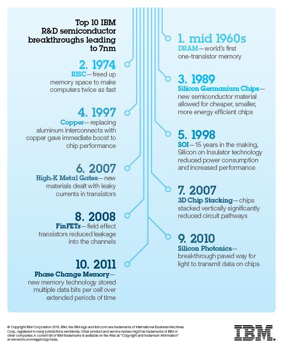
According to IBM the first  7nm chips announced, today was ably possible because of the past breakthroughs listed here (IBM, Twitter)

Microprocessors utilizing 22nm and 14nm technology power today’s servers, cloud data centers and mobile devices, and 10nm technology is well on the way to becoming a mature technology. The IBM Research-led alliance achieved close to 50 percent area scaling improvements over today’s most advanced technology, introduced SiGe channel material for transistor performance enhancement at 7nm node geometries, process innovations to stack them below 30nm pitch and full integration of EUV lithography at multiple levels. These techniques and scaling could result in at least a 50 percent power/performance improvement for next generation mainframe and POWER systems that will power the Big Data, cloud and mobile era.


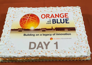
Congratulations to Globalfoundries taking over IBM Chip buisness. Here is a picture from the cake eaten at Globalfoudries to celebrate (Picture from a friend).

“Governor Andrew Cuomo’s trailblazing public-private partnership model is catalyzing historic innovation and advancement. Today’s announcement is just one example of our collaboration with IBM, which furthers New York State’s global leadership in developing next generation technologies,” said Dr. Michael Liehr, SUNY Poly Executive Vice President of Innovation and Technology and Vice President of Research. “Enabling the first 7nm node transistors is a significant milestone for the entire semiconductor industry as we continue to push beyond the limitations of our current capabilities.”

"Today’s announcement marks the latest achievement in our long history of collaboration to accelerate development of next-generation technology," said Gary Patton, CTO and Head of Worldwide R&D at GLOBALFOUNDRIES. "Through this joint collaborative program based at the Albany NanoTech Complex, we are able to maintain our focus on technology leadership for our clients and partners by helping to address the development challenges central to producing a smaller, faster, more cost efficient generation of semiconductors." 

The 7nm node milestone continues IBM’s legacy of historic contributions to silicon and semiconductor innovation. They include the invention or first implementation of the single cell DRAM, the Dennard Scaling Laws, chemically amplified photoresists, copper interconnect wiring, Silicon on Insulator, strained engineering, multi core microprocessors, immersion lithography, high speed SiGe, High-k gate dielectrics, embedded DRAM, 3D chip stacking and Air gap insulators.

IBM and SUNY Poly have built a highly successful, globally recognized partnership at the multi-billion dollar Albany NanoTech Complex, highlighted by the institution's Center for Semiconductor Research (CSR), a $500 million program that also includes the world's leading nanoelectronics companies. The CSR is a long-term, multi-phase, joint R&D cooperative program on future computer chip technology. It continues to provide student scholarships and fellowships at the university to help prepare the next generation of nanotechnology scientists, researchers and engineers.

For more information about SUNY Polytechnic Institute, visit www.sunycnse.com andwww.sunypoly.edu.

Wednesday, July 8, 2015

MIT develops Supercapacitors from Niobium Nanowire Yarns for wearable electronics

As reported by MIT News : Wearable electronic devices for health and fitness monitoring are a rapidly growing area of consumer electronics; one of their biggest limitations is the capacity of their tiny batteries to deliver enough power to transmit data. Now, researchers at MIT and in Canada have found a promising new approach to delivering the short but intense bursts of power needed by such small devices.

The key is a new approach to making supercapacitors — devices that can store and release electrical power in such bursts, which are needed for brief transmissions of data from wearable devices such as heart-rate monitors, computers, or smartphones, the researchers say. They may also be useful for other applications where high power is needed in small volumes, such as autonomous microrobots.

The new approach uses yarns, made from nanowires of the element niobium, as the electrodes in tiny supercapacitors (which are essentially pairs of electrically conducting fibers with an insulator between). The concept is described in a paper in the journal ACS Applied Materials and Interfaces by MIT professor of mechanical engineering Ian W. Hunter, doctoral student Seyed M. Mirvakili, and three others at the University of British Columbia.

Here below is the abstract for the publication or you can continue reading the story from MIT News.

High-Performance Supercapacitors from Niobium Nanowire Yarns

Seyed M. Mirvakili, Mehr Negar Mirvakili, Peter Englezos, John D. W. Madden, and Ian W. Hunter

ACS Appl. Mater. Interfaces, 2015, 7 (25), pp 13882–13888
DOI: 10.1021/acsami.5b02327


The large-ion-accessible surface area of carbon nanotubes (CNTs) and graphene sheets formed as yarns, forests, and films enables miniature high-performance supercapacitors with power densities exceeding those of electrolytics while achieving energy densities equaling those of batteries.1−7 Capacitance and energy density can be enhanced by depositing highly pseudocapacitive materials such as conductive polymers on them.3,8−15 Yarns formed from carbon nanotubes are proposed for use in wearable supercapacitors.3,16 In this work, we show that high power, energy density, and capacitance in yarn form are not unique to carbon materials, and we introduce niobium nanowires as an alternative. These yarns show higher capacitance and energy per volume and are stronger and 100 times more conductive than similarly spun carbon multiwalled nanotube (MWNT) and graphene yarns.6,17−22 The long niobium nanowires, formed by repeated extrusion and drawing,17 achieve device volumetric peak power and energy densities of 55 MW·m–3 (55 W·cm–3) and 25 MJ·m–3 (7 mWh·cm–3), 2 and 5 times higher than that for state-of-the-art CNT yarns, respectively.3 The capacitance per volume of Nb nanowire yarn is lower than the 158 MF·m–3 (158 F·cm–3) reported for carbon-based materials such as reduced graphene oxide (RGO) and CNT wet-spun yarns,5 but the peak power and energy densities are 200 and 2 times higher, respectively.5 Achieving high power in long yarns is made possible by the high conductivity of the metal, and achievement of high energy density is possible thanks to the high internal surface area. No additional metal backing is needed, unlike for CNT yarns and supercapacitors in general, saving substantial space. As the yarn is infiltrated with pseudocapacitive materials such as poly(3,4-ethylenedioxythiophene) (PEDOT), the energy density is further increased to 10 MJ·m–3 (2.8 mWh·cm–3). Similar to CNT yarns, niobium nanowire yarns are highly flexible and show potential for weaving into textiles and use in wearable devices.

Atomic layer deposition technology finds path to medical market via drug-delivery systems

I know I covered this before but it is just so cool technology. Just take a moment and think about all the possibilities and how big this market is. Here is another angle on the story - Republished form : Plastics Today

Atomic layer deposition technology finds path to medical market via drug-delivery systems


Finland-based supplier of atomic layer deposition (ALD) technology Picosun Oy (Espoo) recently announced that it has entered the medical market via drug-delivery systems developed by Nanexa AB (Uppsala, Sweden).


ALD enables the deposition of hermetic, ultra-thin layers of metals, polymers and other materials on a range of products. The technology's capability to cover very small parts with complex geometries gives it an attractive profile for medical device applications. The coating increases operational life, reliability and safety of medical equipment and enables advanced synthesis, delivery and dosing of medical substances, says the company. Several biocompatible coating materials are available, and because it is a gas-phase, low-temperature method, the ALD process can be used to coat sensitive plastic substrates in medical products. Picosun did not disclose the specific material used in the Nanexa application.

Nanexa is specialized in the development of nanotechnology-enabled drug-delivery systems that, it says, "create new possibilities for drug formulations and drug release." Its signature PharmaShell technology encapsulates solid drug particles in the nano- to micrometer range within an extremely thin shell made from a soluble, mineral compound. The thickness of the shell determines the time-release properties and allows precise therapeutic tailoring. The shell, which is created by ALD technology, completely dissolves and exits the body.

Picosun ALD process tools are used primarily in the semiconductor industry as well as in microelectromechanical and light-emitting diode production. The technology also has applications in the deposition of protective, decorative and biocompatible coatings, and is widely used in high-level research institutes across the world.

Picosun would like to see its technology make further inroads into medical applications. To this point, it is involved in the InForMed project, a European Union (EU) initiative to develop an integrated micro-fabrication pilot line for medical device production that incorporates the full innovation chain from concept to system qualification. The project, which is funded by the EU ECSEL JU public-private partnership, began in June 2015 and runs until May 2018.

PneumatiCoat completes DOE Project for a Battery Pilot Plant and recieves US Navy funding

Battery cathode materials with improved safety and performance. Picoshield® coatings provide improvements on many of the most common Li-ion cathode materials used today. As the leader in ALD battery materials PneumatiCoat (PCT) can attain cutting edge performance out of existing battery materials, both cathode and anode. 

Recently has had success in finalizing and receiving additional DOE funded projects as reported here:

PCT Presenting at DOE Annual Merit Review in Arlington, VA

June 2015 - PCT is presenting the most recent results from our DOE Phase II project. With the completion of our pilot plant, large format Picoshield® battery cells are built and producing excellent data. The results expand on the positive work conducted during the Phase I by proving out the quality, consistency, and throughput achievable using our high throughput system. The Annual Merit Review showcases DOE funded research in the fields of hydrogen, fuel cells, and vehicle technologies.

PCT Awarded NAVY SBIR Phase I for "Long Lasting, Highly Efficient, and Safe Batteries for Sensor Systems"

June 2015 - Pneumaticoat Technologies has been awarded a DOD Phase I SBIR from the Navy to develop improved batteries for sensor systems. This work will focus on improving the overall safety of the battery systems and improving the lifetime performance of critical, battery operated, sensors. Picoshield® coatings will play a crucial role in improving battery performance.
More informsation can be found here: http://www.pneumaticoat.com/news.html 


By incorporating well established manufacturing principles (continuous vs. batch, variable throughput vs. fixed throughput, etc.), PneumatiCoat Technologies has developed an efficient and cheap process for precise coating of powders, flats, and objects. Thanks to our innovative process design and system building know-how, Pneumaticoat Technologies is pushing the boundaries of ALD for manufacturing. With our technology, the days of ALD being too slow and too expensive are over. With high throughput manufacturing capabilities, at inexpensive price points, a great majority of the application technologies that were "put on the shelf" can now be reconsidered as viable commercial products. Combined with the exponential growth in application R&D, PneumatiCoat Technologies' systems are well-poised to help usher in a new wave of customized products to market. (http://www.pneumaticoat.com)

Tuesday, July 7, 2015

Integration of Sub-10 nm ALD Gate Oxide on MoS2 with Ultra Low Leakage and Enhanced Mobility

Here is a nice Open Source report (Scientific Reports 5, Article number: 11921 (2015) doi:10.1038/srep11921) on integration of Sub-10 nm Gate Oxide on MoS2 with Ultra Low Leakage and Enhanced Mobility. 

Atomic layer deposition of Al2O3 on MoS2 flakes was performed according to the paper, some of the MoS2 flakes were loaded into the Picosun R200 ALD chamber for direct Al2O3 deposition. During the deposition, TMA and H2O served as the aluminum and oxygen precursors, respectively, and different growth temperatures and pulse time were adopted to observe their impacts. For some of the flakes, the remote O2 plasma pretreatments were carried out in the same chamber before Al2O3 was deposited.


(a) Cross-sectional schematic of the top-gated devices together with the electrical connections. (b) Ids – Vtg curves with Vds ranging from 50 mV to 500 mV. The inset shows the Ids – Vds curves with the top gate voltages of 0 V and 2 V. (c) Top gate leakage current of the device. Optical image of the top gate device is attached as the inset of (c). Top gate dielectric of this device is 60 cycles Al2O3 deposited with 60 s remote oxygen plasma pretreatment. All these measurements were performed at room temperature with the back gate grounded (Scientific Reports 5, Article number: 11921 (2015) doi:10.1038/srep11921) .

Redeposition effects in plasma-assisted atomic layer deposition

Here it is - a very important study published by Oxford Instruments and TU Eindhoven on "redeposition effects" in plasma-assisted atomic layer deposition - not to be confused with "CVD effects" or "thermal decomposition of precursor effects" or other disturbing effects make the life as a ALD process guy non-conformal.

Redeposition in plasma-assisted atomic layer deposition: Silicon nitride film quality ruled by the gas residence time 

Harm C. M. Knoops, K. de Peuter and W. M. M. Kessels
Appl. Phys. Lett. 107, 014102 (2015); http://dx.doi.org/10.1063/1.4926366

The requirements on the material properties and growth control of silicon nitride (SiN x ) spacer films in transistors are becoming ever more stringent as scaling of transistor structures continues. One method to deposit high-quality films with excellent control is atomic layer deposition (ALD). However, depositing SiN x by ALD has turned out to be very challenging. In this work, it is shown that the plasma gas residence time τ is a key parameter for the deposition of SiN x by plasma-assisted ALD and that this parameter can be linked to a so-called “redeposition effect”. This previously ignored effect, which takes place during the plasma step, is the dissociation of reaction products in the plasma and the subsequent redeposition of reaction-product fragments on the surface. For SiN x ALD using SiH2(NH t Bu)2 as precursor and N2 plasma as reactant, the gas residence time τ was found to determine both SiN x film quality and the resulting growth per cycle. It is shown that redeposition can be minimized by using a short residence time resulting in high-quality films with a high wet-etch resistance (i.e., a wet-etch rate of 0.5 nm/min in buffered HF solution). Due to the fundamental nature of the redeposition effect, it is expected to play a role in many more plasma-assisted ALD processes.

Photo show from EuroCVD 20 in Sempach

Here all pictures that appear on Twitter (#EuroCVD), Facebook, LinkedIn or that people send me (jonas.sundqvist@baldengineering.com) will be collected!
Main page of Euro CVD 20 : http://eurocvd20.empa.ch/index.html 

Impressions


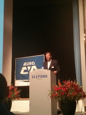
Prof. Hoffman opening the Euro CVD and the famous CVD flag hanging in the background (Photo by Henrik Pedersen)


HERALD Flyers! (Twitter, Henrik Pedersen)


Hoffman and Devi presented HERALD (Twitter, Henrik Pedersen)


Michael Hitchman makes a big announcement: after 20 years, he will retire as the editor of the journal CVD (Twitter, Sean Barry)


Seminars


Don´t miss the talk by Henrik Pedersen, Department of Physics, Chemistry and Biology, Linköping University, making an effort to unite us all "A combined ALD-CVD route for group 13 nitride based high frequency devices" Thursday 16 July, 09:30. Here a preview of the talk in the making (Twitter, Henrik Pedersen).


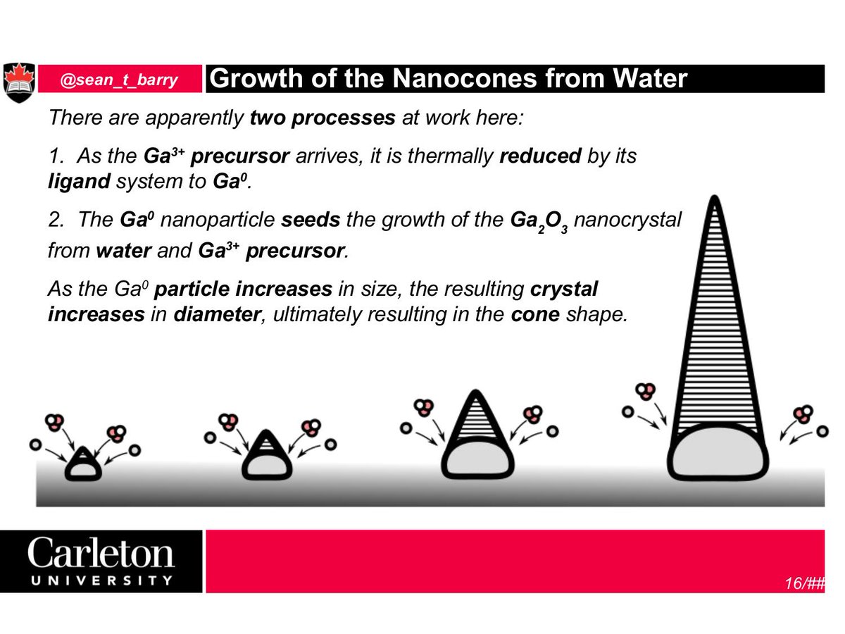
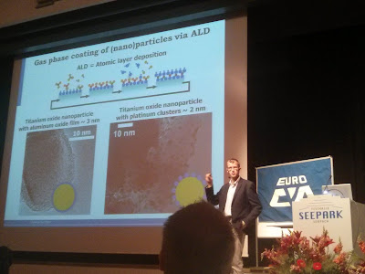
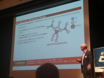
Preview slide from Sean Barry "Growth of Nanocones from Water" (shared on Twitter)


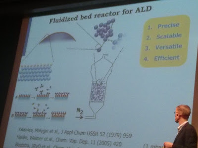
Ruud van Ommen giving his talk on ALD on nano powders using Fluidized bed reactors first publish in Russia 1979 (Photo by Henrik Pedersen)


Talk by Sean Barry on seedless GaO nano wire growth by pulsed CVD (Photo by Henrik Pedersen)


New ketoiminate Y precursors from Devi's group and for yttria stabilized cubic hafnia by ALD and post deposition anneal (Twitter, Henrik Pedersen)


The talk by Prof. Pedersen from Linköping University on combining ALD and CVD for InN (Twitter, Sean Barry)


Ending of Euro CVD Twenty by Prof. Hoffmann (Twitter, Louise)


Poster sessions


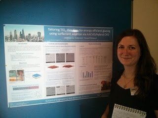
Ann-Louise Andersson at her poster on TiO2 AACVD / Hybrid CVD using surfactants (Photo by Henrik Pedersen)

Trade show


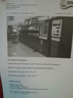
Free Aixtron MOCVD System (Henrik Pedersen)

Dinners and Receptions


Mini golf tournament (Twitter, Russell Binions)


Sightseeing


Sempach is a cute little town (Sean Barry, Twitter).


The gathering of ducks in the CVD Duck Pond - Euro CVD!  (Picture by Sean Barry, from Twitter)


A typically Swiss picture (Twitter, Russel BinIons)


Scenic Sempach (Twitter, Sean Barry)


Local gun shop  (Henrik Pedersen)


Boat cruise on the Sempach Lake (Henrik Pedersen)


UPDATE - Atomic Layer Deposition Precursor Suppliers

ALD Pulse has updated the ever growing list of ALD precursor suppliers - the list is reproduced below however for the most up to date version always go here: http://aldpulse.com/chemical-suppliers-view


Air Liquide is a leading supplier of precursors for Atomic Layer Deposition.
Strem is a leading supplier of precursors for Atomic Layer Deposition.
 Praxair is a leading supplier of precursors for Atomic Layer Deposition.
Tanaka is a leading supplier of precursors for Atomic Layer Deposition.
Sigma Aldrich is a leading supplier of precursors for Atomic Layer Deposition.
ATMI  is a leading supplier of precursors for Atomic Layer Deposition.
Nova-Kem is a leading supplier of precursors for Atomic Layer Deposition.
TOSOH is a leading supplier of precursors for Atomic Layer Deposition.
Air Products is a leading supplier of precursors for Atomic Layer Deposition.
Adeka is a leading supplier of precursors for  Atomic Layer Deposition.
Precision Molecular Design Corporation is a leading supplier of precursors for Atomic Layer Depos
DOW Electronic Materials is a leading supplier of precursors for Atomic Layer Deposition
UP Chemical Co; Ltd. is a leading supplier of precursors for Atomic Layer Deposition
EpiValence is a leading supplier of precursors for Atomic Layer Deposition.
Volatec is a leading supplier of precursors for Atomic Layer Deposition.
Pegasus Chemicals is a leading supplier of precursors for Atomic Layer Deposition.
Dock/Chemicals is a leading supplier of precursors for Atomic Layer Deposition.
Ereztech is a leading supplier of precursors for Atomic Layer Deposition.
Gelest is a leading supplier of precursors for Atomic Layer Deposition.
Japan Advanced Chemicals is a leading supplier of precursors for Atomic Layer Deposition.
Seastar Chemicals Inc. is a leading supplier of precursors for Atomic Layer Deposition.