Showing posts with label Semiconductor. Show all posts

Tuesday, August 22, 2023

Indo-Pacific Region's Pivotal Role in Global Semiconductor Industry Supply Chain

Mapping the Semiconductor Supply Chain: The Critical Role of the Indo-Pacific Region

The report underscores the Indo-Pacific region's paramount role in the complex global semiconductor supply chain. Across various stages, from design to fabrication, the report illuminates the region's indispensable contributions to the industry's functionality and the wider impact on global economics and geopolitics.

The report highlights semiconductors' critical position in the world economy, impacting sectors like electronics and infrastructure. With annual sales surpassing half a trillion dollars and a far-reaching economic impact, recent events like the semiconductor shortage, causing a $240 billion GDP reduction and halting auto production, underscore this centrality.

The analysis delves into the intricate facets of the semiconductor supply chain, spotlighting the collective influence of Taiwan, Japan, China, and South Korea. These Indo-Pacific nations specialize in semiconductor design, fabrication, and more, with the United States as a significant player, reflecting its Pacific power status and industry leadership.

The authors unravel the complexities of design, fabrication equipment, materials, and assembly. They emphasize the U.S.'s lead in design software and intellectual property. The report also uncovers the Indo-Pacific's domination of manufacturing equipment, especially by the U.S., Japan, and South Korea.

Geopolitically, the report discusses how national strategies adapt to ensure resilient supply chains and technological sovereignty. It underscores the need for collaboration, particularly in the Indo-Pacific, to build robust ecosystems that counter risks and ensure secure supply chains.

Materials and Chemicals: Cornerstones of Semiconductor Manufacturing

The semiconductor industry's core relies on vital raw and manufactured materials like silicon wafers, photomasks, and photoresists, as well as crucial chemicals in the manufacturing process. The market for these fabrication materials exceeded $40 billion in 2021, concentrated mainly in the United States, Germany, Japan, Taiwan, South Korea, and China. Taiwan claimed the largest share with 25%, while Europe and China had smaller shares. Silicon wafers, forming a significant portion of the market, are essential components for semiconductor production. Their market has evolved over two decades, with five companies now controlling 95% compared to over 20 in 1990. 


Key players in silicon wafer manufacturing include Japanese, Taiwanese, German, South Korean, and French firms. While China's presence is growing, its ability to produce 300 mm/12-inch silicon wafers remains limited. Photomasks and photoresists, integral to semiconductor fabrication, are mainly dominated by Japanese, Taiwanese, and South Korean companies. China's progress in these areas has been notable, marked by investments aimed at enhancing their capabilities. The report highlights these materials' significance within the complex semiconductor supply chain and underscores the Indo-Pacific's pivotal role in their production and distribution.

Semiconductor Manufacturing Equipment: Key Players and Indo-Pacific Dominance

Summary: The semiconductor manufacturing process relies on highly specialized equipment to create intricate integrated circuits on silicon wafers. The Indo-Pacific region dominates the semiconductor manufacturing equipment (SME) market, contributing to 77% of global SME sales. The United States and Japan lead in SME production, with South Korea also playing a significant role. The United States and Japan excel in producing wafer fabrication equipment, while Japan has a strong presence in assembly and test equipment. 

China is a major player in assembly, test, and packaging (ATP) equipment, particularly through companies like ASM Pacific. The Indo-Pacific region is home to the majority of semiconductor fabrication facilities, with China rapidly expanding its fabrication capabilities. Additionally, ATP facilities are concentrated in the Indo-Pacific region, with Taiwan, China, and Southeast Asia (including countries like Singapore, Malaysia, Vietnam, and the Philippines) being key contributors. ATP facilities encompass processes such as chip cutting, testing, and assembling, and while these processes may be less complex compared to other stages of manufacturing, they have become more intricate with the continual shrinking of transistor size and density in semiconductor chips.

In summary, the report unveils the Indo-Pacific's pivotal role in the global semiconductor industry. By dissecting the supply chain and revealing its geopolitical implications, the report serves as a vital resource for policymakers and industry stakeholders in navigating this dynamic landscape.

TSMC's 2nm Chip Plant Faces Delays in Taichung, Water and Electricity Hurdles Cited

Taiwan Semiconductor Manufacturing Company (TSMC) is experiencing setbacks in the construction of its highly anticipated 2-nanometer chip manufacturing plant in Taichung City, Taiwan. Delays have been attributed to challenges related to water and electricity supply, crucial for the resource-intensive chip fabrication process. This development comes as TSMC seeks to expand its manufacturing capabilities amid a rapidly evolving semiconductor landscape.

aiwan Semiconductor Manufacturing Company (TSMC), a global leader in semiconductor manufacturing, is facing delays in the construction of its planned 2-nanometer chip manufacturing plant in Taichung City, Taiwan. The director of the agency responsible for managing science and technology infrastructure on the island has indicated that the construction will not commence by the end of this year.

TSMC initially intended to establish two 2-nanometer manufacturing sites in Taiwan, with the first site in Hsinchu City. However, due to delays in the approval process for the Taichung site, the company confirmed its decision to also manufacture next-generation chips in Kaohsiung City.

The primary challenges affecting the Taichung site relate to the plant's water and electricity requirements. Chip fabrication demands high-purity conditions, necessitating large volumes of pure water to meet product purity standards. TSMC has encountered obstacles in securing an adequate water supply, particularly during a 2021 drought that led the company to employ water tankers to fulfill its water needs.

These developments underscore the intricate logistical challenges inherent in semiconductor manufacturing, where resource-intensive processes require precise environmental conditions. While TSMC continues to innovate and expand its global operations, addressing these challenges becomes paramount to maintaining its position at the forefront of the semiconductor industry.

Thursday, July 13, 2023

2023 Semiconductor Materials Market Slowing but Resilient

Material growth to resume in 2024 as industry recovers and fabs ramp up

San Diego, CA, July 12, 2023: TECHCET—the electronic materials advisory firm providing business and technology information— announced that the Total Semiconductor Materials market will contract by at least -3% in 2023 given the industry wide slowdown and reported higher levels of inventory in the materials supply chain. This year’s decline will result in revenues for Semiconductor Materials to total US$69.6 billion, down from the US$71.7 reported in 2022. However, leading-edge logic and automotive/power device production will limit the overall decline in materials revenues for 2023.
TECHCET is forecasting a strong recovery in the market in 2024, with total material revenues increasing 8% to almost US$75 billion. CAGR growth over the next 5 years is forecasted to be 4%, which will result in the market reaching US$88 billion by 2027.


To read the full article, go to: https://lnkd.in/gVan5qSq

To find out more: see TECHCET at SEMICON West at NY CREATES Booth (North Hall 5845) from July 11-13. Lita Shon-Roy, Diane Scott, Dan Tracy, and Kevin McLaughlin will all be there to share market insights and industry updates. Or visit our website here: https://lnkd.in/gJQ2Gt36.

Segment summarized by TECHCET previous recent releases:

Semiconductor Metal Plating Chemicals:

The market for semiconductor metal plating chemicals is expected to experience a slight decrease of 2% in 2023. This decline is due to lower expectations for overall wafer starts and inventory corrections within the market. Copper is the largest revenue contributor in this segment, particularly in advanced packaging wiring and interconnect copper plating. However, the market is expected to rebound in the long term, with a positive compound annual growth rate (CAGR) of 3.7% for advanced packaging and 3.3% for interconnect metal chemicals.

Semiconductor Quartz Equipment Components:

After reaching an all-time high in 2022, the market for fabricated quartz equipment components is expected to decline in 2023. The slowdown is attributed to a shift in industry investments and reduced purchase orders. However, the market is buoyed by previous purchases and backlogs, leading to a projected decline of 6% in 2023. New fab expansions are expected to drive future growth, with a CAGR of 5% from 2022 to 2027.

CMP Consumables:

Following strong performance in 2022, the CMP consumables market is forecasted to experience a slight reduction of 2.4% in 2023. The decrease is primarily due to oversupply in DRAM and market corrections. However, the market is expected to achieve a 5-year CAGR of 5.2%. The demand for new metals pads and slurry is anticipated to drive growth in this segment, particularly with the development of advanced logic methodologies and the evaluation of new BEOL materials.

Electronic Gases:

The electronic gases market is expected to witness a positive 5-year CAGR of 6.4% driven by expansions within the semiconductor industry, especially in leading-edge logic and 3DNAND applications. However, supply constraints for critical gases like B2H6 and WF6 may arise as demand outpaces supply. Disruptions in gas supply from current sources and geopolitical events may lead to shortages. Helium supply is also considered at high risk. Despite these challenges, the market is projected to grow, particularly with new fab expansions and increasing demand.

Semiconductor Wet Chemicals:

Semiconductor wet chemical revenues are forecasted to decline by 2% in 2023, following the trends in wafer starts and rising energy prices. The industry slowdown and instability from the Russia-Ukraine war contribute to the market contraction. However, the market is expected to rebound in 2024, with a 5-year CAGR of 3.9%. Phosphoric acid is the strongest segment within wet chemicals due to growth in the 3DNAND market. A holistic approach to the chemical supply chain is crucial for success in this market.

ALD/CVD Precursors:

The market for ALD/CVD precursors experienced a flattening in 2023 due to reduced memory pricing in production. However, a rebound is expected in the second half of the year, driven by the recovery of memory pricing. The market for high-ƙ and low-ƙ dielectric precursors is projected to rebound significantly in 2027, with a growth rate of approximately 19%. The market will be boosted by fab expansions, logic advancements, and increasing demand for metal and dielectric precursors.

Tuesday, June 13, 2023

Global 300mm Fab Equipment Spending to Reach Record $119 Billion in 2026, Fueled by Strong Demand for High-Performance Computing and Automotive Applications

 Korea Leads the Way, Foundry and Memory Sectors Drive Expansion

  • Global 300mm fab equipment spending is projected to reach a record high of $119 billion in 2026, driven by strong demand for high-performance computing, automotive applications, and improved memory requirements.
  • Korea is expected to lead global 300mm fab equipment spending in 2026, followed by Taiwan, China, and the Americas, with the foundry and memory sectors playing significant roles in the expansion.
The global 300mm fab equipment spending is expected to soar to an unprecedented level of $119 billion by 2026, after experiencing a temporary decline in 2023. This remarkable growth is primarily attributed to the surging demand for high-performance computing and automotive applications, coupled with an overall improvement in the demand for memory.


The foundry and memory sectors are poised to be major catalysts in this expansion, signaling a widespread need for semiconductor chips across various end markets and applications. These sectors will drive significant investment in 300mm fab equipment, ensuring the industry's capacity to meet the escalating demand.

In terms of regional spending, Korea is anticipated to lead the global 300mm fab equipment market in 2026. With its well-established semiconductor industry and technological prowess, Korea is well-positioned to capitalize on the increasing demand for chips. Following closely behind Korea, Taiwan, China, and the Americas are expected to contribute substantially to the global spending.

Among the different segments, the foundry sector is projected to witness the highest equipment spending. As the demand for custom-designed chips continues to surge, foundries will invest heavily in advanced manufacturing equipment to meet the diverse needs of their customers. The memory sector is also set to experience robust equipment spending, driven by the growing demand for high-capacity memory solutions in various applications, including data centers, artificial intelligence, and Internet of Things (IoT) devices.

While the foundry and memory sectors thrive, other segments may face modest growth or even decline. This suggests a shifting landscape within the semiconductor industry, with specific sectors driving the overall growth while others adapt to changing market dynamics.

In conclusion, the global 300mm fab equipment spending is poised to reach unprecedented heights in 2026, driven by the strong demand for high-performance computing, automotive applications, and improved memory requirements. Korea is expected to lead the global spending, with the foundry and memory sectors playing pivotal roles in the expansion. This remarkable growth underscores the critical importance of semiconductor chips across a wide range of industries and highlights the need for substantial investment in advanced manufacturing capabilities to meet future demands.

Thursday, June 8, 2023

Global semiconductor equipment billings rise 9% YoY to $26.8B in Q1 2023. Taiwan up 42%, China down 8%, North America soars 51%. Strong AI and automotive investments.

US Fab expansion kick in - The global semiconductor equipment billings rose 9% YoY to $26.8B in Q1 2023, despite challenging conditions. Taiwan saw 42% growth, while China dropped 8%. North America surged by 51%. Long-term investments for AI and automotive remain strong.


As an excerpt from a news release by SEMI - here are some key points from the report:

Global Semiconductor Equipment Billings - In the first quarter of 2023, global semiconductor equipment billings reached US$26.8 billion, representing a 9% increase compared to the same period in the previous year. However, billings slipped 3% when compared to the previous quarter.

Regional Billings

The data provided breaks down the billings by region and shows the quarter-over-quarter and year-over-year changes. Here are some notable regional highlights:Taiwan: Billings of $6.93 billion, with a 13% decrease compared to the previous quarter but a significant 42% increase year-over-year.

  • China: Billings of $5.86 billion, reflecting an 8% decrease quarter-over-quarter and a 23% decrease year-over-year.
  • Korea: Billings of $5.62 billion, showing a slight 3% decrease quarter-over-quarter but a positive 9% increase year-over-year.
  • North America: Billings of $3.93 billion, indicating a substantial 51% increase quarter-over-quarter and a significant 50% increase year-over-year.
  • Japan: Billings of $1.90 billion, with a 16% decrease quarter-over-quarter but no change year-over-year.
  • Europe: Billings of $1.52 billion, reflecting a 4% increase quarter-over-quarter and a 19% increase year-over-year.
  • Rest of World: Billings of $1.06 billion, experiencing a 20% decrease quarter-over-quarter and an 18% decrease year-over-year.
Market Outlook: Despite macroeconomic challenges and a difficult industry environment, semiconductor equipment revenue in the first quarter was robust. The long-term strategic investments needed to support major technology advancements for applications like AI (Artificial Intelligence) and automotive remain healthy.

SEMI Equipment Market Data Subscription (EMDS): SEMI offers a subscription service providing comprehensive market data for the global semiconductor equipment market. It includes monthly reports on equipment market trends, semiconductor equipment billings by region and market segments, and an outlook for the semiconductor equipment market.

https://semi.org/en/news-media-press-releases/semi-press-releases/q1-2023-global-semiconductor-equipment-billings-grow-9%25-year-over-year-semi-reports

Tuesday, May 2, 2023

Global Semiconductor Sales Decrease 8.7% in First Quarter; March Sales Tick Up Month-to-Month for First Time Since May 2022

Semiconductor sales continued to slip during the first quarter of 2023 due to market cyclicality and macroeconomic headwinds, but month-to-month sales were up in March for the first time in nearly a year, providing optimism for a rebound in the months ahead.

WASHINGTON—May 1, 2023—The Semiconductor Industry Association (SIA) today announced worldwide sales of semiconductors totaled $119.5 billion during the first quarter of 2023, a decrease of 8.7% compared to the fourth quarter of 2022 and 21.3% less than the first quarter of 2022. Sales for the month of March 2023 increased 0.3% compared to February 2023. Monthly sales are compiled by the World Semiconductor Trade Statistics (WSTS) organization and represent a three-month moving average. SIA represents 99% of the U.S. semiconductor industry by revenue and nearly two-thirds of non-U.S. chip firms.


“Semiconductor sales continued to slip during the first quarter of 2023 due to market cyclicality and macroeconomic headwinds, but month-to-month sales were up in March for the first time in nearly a year, providing optimism for a rebound in the months ahead,” said John Neuffer, SIA president and CEO.

Regionally, month-to-month sales increased in Europe (2.7%), Asia Pacific/All Other (2.6%), and China (1.2%), but decreased in Japan (-1.1%) and the Americas (-3.5%). Year-to-year sales decreased across all regions: Europe (-0.7%), Japan (-1.3%), the Americas (-16.4%), Asia Pacific/All Other (-22.2%), and China (-34.1%).

For comprehensive monthly semiconductor sales data and detailed WSTS forecasts, consider purchasing the WSTS Subscription Package. For detailed historical information about the global semiconductor industry and market, consider ordering the SIA Databook.

Thursday, September 29, 2022

The Semiconductor Climate Consortium founded by SEMI and memebers

The Semiconductor Climate Consortium publicly recognizes the challenge of climate change and works to speed industry efforts to reduce greenhouse gas emissions in individual company operations, across the value chain, and in other sectors of our value-chain, including the industries our products enable.

We believe that member companies, with our accumulated knowledge and innovative technology, working collaboratively will accelerate solutions for environmental challenges. Working together, we will address and solve issues no one company can do alone.

The Semiconductor Climate Consortium drives progressive climate action through collaboration and alignment, measuring and reporting, and setting ambitious target for Net Zero to keep global climate change within 1.5°C.

More information on the consortium and on how to join you may find here: Semiconductor Climate Consortium | SEMI


There is also a 2-year effort for Start-Ups that started already a year ago, where AlixLabs and NSS Water from Sweden participated with groundbreaking technology and reached the Pitch Semifinals with 18 other contenders. The 9 winners are announced here (and below): Startups for Semiconductor Sustainability Finalists Announced in Next Step to Greener Chip Industry | SEMI


Global fab equipment spending is expected to increase 9% YOY to a new all-time high of US$99 billion in 2022

MILPITAS, Calif. — September 27, 2022 — Global fab equipment spending for front-end facilities is expected to increase approximately 9% year-over-year (YOY) to a new all-time high of US$99 billion in 2022, SEMI announced today in its latest quarterly World Fab Forecast report. The report also shows the global fab equipment industry increasing capacity this year and again in 2023.

“After achieving a record level in 2022, the global fab equipment market is projected to remain healthy next year driven by new fabs and upgrade activity,” said Ajit Manocha, SEMI President and CEO.


Wednesday, September 28, 2022

ALD Enabling Quartz Part Recycling for Semiconductor Processing Equipment

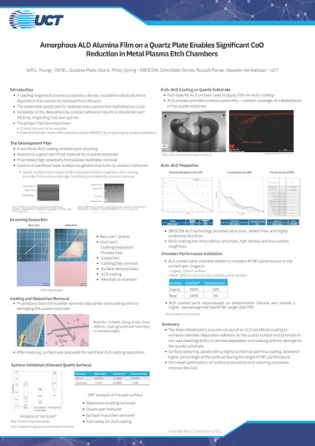
[Reposted from UCT Blog, LINK] In a manufacturing environment, productivity is dependent on predictability, and keeping operating equipment to a scheduled maintenance interval is the key to meeting performance targets.

For many chambers, in-situ cleaning is not an option to manage by-product buildup, and the scheduled preventative maintenance (PM) cycle involves replacing parts to maintain specifications. Ideally, the parts removed from a chamber are cleaned and returned to the fab for reuse, minimizing the cost of ownership (CoO) for the tool.

Crystalline Al2O3 by-product and trace metals deposited on quartz parts in etch chambers raise an issue as they can peel and cause particle problems leading to un-scheduled chamber downtime. It is very important to remove these by-products and trace metals from the quartz parts on a regular basis during PM. However, stripping crystalline Al2O3 (and trace metals) from quartz without compromising the quartz substrate can be a challenge.

In order to address this problem, UCT and a chipmaking customer worked with coating partner Inficon to come up with a novel solution. This solution involved coating the quartz parts with a sacrificial atomic layer deposition (ALD) film and developing a cleaning and texturing refurbishment process.

ALD is used broadly within semiconductor devices, but ALD films are not used on the parts within production chambers. A high quality, conformal ALD film and a cleaning process with high selectivity to the quartz base material would be ideal to enable by-product removal. Texturing the surface would increase the mechanical adhesion of the by-product layer, reducing the risk of delamination. The highly conformal nature of the ALD film maintains the target surface texture and helps manage surface trace metals.

These quartz parts with a specified surface roughness were coated with at least 200nm of amorphous ALD Al2O3 films. After running in a chamber under process conditions, the by-product coated parts underwent a proprietary chemical strip process developed to remove the ALD Al2O3 film and by-product deposition. The quartz substrate showed no degradation as characterized using x-ray fluorescence (XRF), particle level, and roughness measurements.


This process is now qualified with the customer and the recycled quartz parts provide >75% reduction in Cost of Ownership (CoO). The ALD material was >99.999% pure, fully amorphous, and had a low intrinsic surface roughness. The delamination failure, which typically impacts 16% of all installed parts, was eliminated and a higher percentage overall of the quartz parts met mean time between clean (MTBC) target or full PM. The results were presented at the 2022 ALD/ALE conference with the above poster.

Monday, September 26, 2022

Bottom-up PEALD of SiO2 by growth inhibition for seamless gap-fill process

Bottom-up plasma-enhanced atomic layer deposition of SiO2 by utilizing growth inhibition using NH3 plasma pre-treatment for seamless gap-fill process

Yoenju Choi, Taehoon Kim, Hangyul Lee, Jusung Park, Juhwan Park, Dongho Ryu & Woojin Jeon

Scientific Reports volume 12, Article number: 15756 (2022)

The design-rule shrinkage in semiconductor devices is a challenge at every step of the integration process. In the gap-fill process for isolation, the seam and void formation cannot be suppressed by using a deposition process, which even has excellent step coverage. To achieve seamless gap fill in the high-aspect-ratio structure, which has a non-ideal etch profile such as a negative slope, the deposition process should be able to realize the “bottom-up growth” behavior. In this work, the bottom-up growth of a SiO2 plasma-enhanced atomic layer deposition (PE-ALD) process in a trench structure was investigated by using a growth inhibition process employing plasma treatment. N2 and NH3 plasma pre-treatments were employed to suppress the growth of the SiO2 PE-ALD process without any contamination, and the inhibition mechanism was investigated by performing surface chemistry analyses using X-ray photoelectron spectroscopy. Furthermore, the gap-fill characteristics of the SiO2 PE-ALD process were examined, depending on the process conditions of NH3 plasma pre-treatment, by performing cross-sectional field emission scanning electron microscopy measurements. Finally, a seamless gap-fill process in a high-aspect-ratio trench pattern was achieved by the bottom-up growth behavior of SiO2 PE-ALD using NH3 plasma pre-treatment.


Sunday, September 4, 2022

Tokyo Electron is forcastiong high continued sales in semiconductor equipment sales 2023 - slow down in DRAM

Tokyo electron forecast for FY2023 SPE Division New Equipment Sales Forecast - DRAM is retracting in 2023 but you can´t say that about Logic and Non-Volatile Memory (3DNAND Flash). Full power ahead for ALD and its friends!


One good freind of ALD is Etch. Tokyo Electron is spending quite some development Yen Billions by building a new facility just for etch development.


Saturday, September 3, 2022

ASM reports that the ALD market is expected to grow by a CAGR of 16%-20% from 2020 to 2025

ASM International presented its Q2/2022 report in July and a new record orders of EUR 943 million driven by robust new node spending in logic/foundry and by recent wins in memory, particularly for ALD gap-fill in 3D-NAND and continued adoption of HKMG in DRAM.


ASM focuses on the single wafer market so the numbers presented does typically not include ALD Large Batch, which is dominated by Tokyo Electron and Kokusai. Back in 1999, ASM acquired Finnish legendary ALD company Microchemistry and its Pulsar 2000 cross-flow chamber ALD technology, which later took the market as the 300 mm version Pulsar 3000 for HfO2 in HKMG at Intel, TSMC, Samsung Globalfoundries, and others. Now it is interesting to follow how the success story continues also for DRAM HKMG. Since then, ASM has added PEALD from Genitech (South Korea) and Large Batch ALD (A412), and many other ALD process technologies. See recent announcements 2022 here:


So it is interesting that ASM has launched a new ALD Batch platform based on the now rather old A412 and the new TENZA to capture growth in Gap-fill - a stronghold for Lam Research.

The ALD market is driven by increased wafer starts in 300 mm for sub 45 nm nodes, 3DNAND and DRAM, and the ongoing fab expansions world-wide.


  • TechInsights expects WFE to increase by 21% in 2022 (July 2022)
  • Strongest growth in leading-edge nodes, spending on 7nm and below expected to grow from ~25% of WFE in 2020 to ~42% of WFE in 2025
  • Gartner expects total WFE to increase by 19% in 2022 (July 2022)
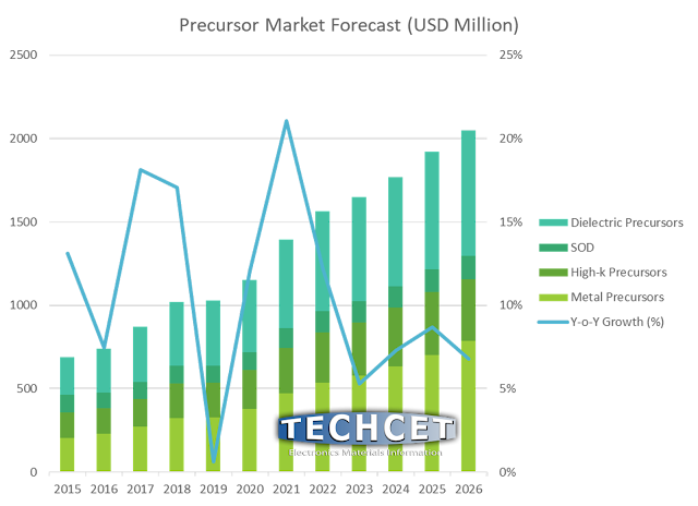
You can compare the TECHCET forecast on precursors where you can see high y-o-y growth going through 2021 and 2023 driven by increased 300 mm wafer production and a slowdown in 2023. Please find deeper dives, assessments and all the data in the TECHCET CMR reports: ALD / CVD Precursors (2) Archives - TECHCET CA LLC


Precursor market forecast 2022-2026 - Invited talk for TECHCET LLC CA in: AA2-TuM2-1 High ALD Equipment and Precursor Demand and 5-Year Forecast Due to Continued Semiconductor Device Scaling and Fab Expansions by Jonas Sundqvist.


Thursday, September 1, 2022

Supply Tightening Expected for Specialty Electronic Gases

Demand to outpace supply for NF3 and WF6 unless alternatives come into play

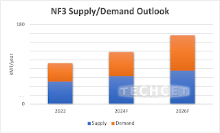
San Diego, CA, August 31, 2022: TECHCET—the electronic materials advisory firm providing business and technology information— reports that the supply of Specialty Gases, nitrogen trifluoride (NF3) and tungsten hexafluoride (WF6) for electronics could tighten amongst high projected demand by 2025-2026. This forecasted steep trajectory will challenge supply-chains to keep pace. However, alternatives being developed could interrupt this trend. Both NF3 and WF6 are part of a larger US$5 billion specialty gas segment forecasted to grow 30% over the next 5 years, to total US$6.5 billion by 2026. As shown below, NF3 is expected to grow even more steeply, 72% over the forecast period (as highlighted in TECHCET’s 2022 Critical Materials Report™ on Electronic Gases).


Alternatives for these gases are currently in development which could cause a shift in growth trends. The increasing demand for NF3 in electronic manufacturing, including flat-panel displays, has triggered concern among atmospheric scientists over emissions of nitrogen trifluoride, a potent greenhouse gas. Particularly, NF3 gas has a high Global Warming Potential (GWP) compared to other gases. Consequently, the electronics industry is looking at and considering processes for on-site fluorine generation that can use F2, in place of NF3, for chamber cleaning.

...

To read the full article, click here: https://lnkd.in/g25Fa3f2

For more information on the electronic gases market outlook, check out our newest Gases Critical Materials Report™ here: https://lnkd.in/gb95EBC

Tuesday, May 10, 2022

Semiconductor Materials at a Critical Tipping Point - Key Industry Issues Revealed

San Diego, CA, May 10, 2022: TECHCET—the electronic materials advisory firm providing business and technology information— held its highly successful and well-attended 2022 Critical Materials Conference in Chandler, Arizona on April 28th and 29th. Over 300 attendees and speakers participated in the event to hear about and to discuss semiconductor material issues and trends that are critical to the entire semiconductor industry supply chain—now and in the future.

2022 CMC Conference Keynote Speaker, John Whitman, Corporate Vice President, Operations Central Team & Procurement at Micron Technologies Corp., and Karey Holland, Ph.D., Sr. Advisor and CMC Conference Co-Chair, TECHCET

The opening keynote for the conference was delivered by John Whitman, Corporate Vice President, Operations Central Team & Procurement; Micron Technologies Corp. and addressed the topic of “Covid Impacts on our Supply Assurance Playbook”. The Covid pandemic and subsequent logistic and other supply chain issues over the past two years have highlighted critical issues for the semiconductor industry. Just-in-time delivery has lessened as a procurement priority, and now manufacturers focus on supply chain stability. It is important for device makers to build their supply chain around Business Continuity Plans (BCP) so to ensure production schedules are maintained.

Industry-wide, there is an opportunity for companies to share information through digitization of supply-chain data. With sharing of information and data, companies across the supply chain can collaborate and solve critical issues with respect to materials delivery and performance, thus optimizing semiconductor processing.

This technical conference includes 5 impactful sessions with focuses on 1) Business Trends & Global Issues, 2) Immediate Challenges of Materials & Manufacturing, 3) Future Challenges for Equipment & Component Processes, 4) Emerging Materials & Processes, and 5) Materials for Advanced Packaging and Heterogeneous Integration.

The Conference has just opened up registration for “After Hours” interaction offering online viewing of presentation videos and pdf downloads, and virtual networking opportunities with other “attendees.”On Day 1, sessions 1 through 3 cover a gamut of topics critical to the semiconductor industry supply chain. Topics from the industry outlook for devices, semiconductor manufacturing equipment and materials, to water supply challenges, green manufacturing initiatives, and workforce development were all discussed.
On Day 2, the event focused on emerging materials applications including materials needed for 3nm and smaller technology nodes as well as material challenges of interposes versus bridges and other issues concerning wafer level modeling materials.

For more information about how to attend the CMC Conference After Hours, go to:

Friday, April 8, 2022

Sneak Peak Into Our New Equipment Components Session at CMC2022 in Chandler AZ April 27-29

Less than 4 Weeks to go for our CMC Conference, April 27-29, Chandler, AZ! Register Now Before It's Too Late!


Here's a Sneak Peak Into Our New Equipment Components Session

-George Alajajian, Ph.D.,VP Strategic Parts Supply Chain, Intel Corp. presenting on "Consumable Equipment Components Requirements for Leading Edge IDMs"

-Dalia Vernikovsky, CEO & GM, Applied Seals NA, Inc presenting on "Polymeric Sealing Properties, Advances & Limitations"

-Jennifer Braggin, Director, CTO’s Office, Entegris presenting on "New filtration and purification technologies for 3nm and beyond for better contamination control and yield improvement"

-Sami Sneck, Vice President, Advanced ALD, Beneq presenting on “Enhancing yield with ALD coatings for critical chamber components”

Coffee / Networking Break - Sponsor: Coexcell with Raffle Giveaway

-Nicole Rutherford, Product Manager, Greene Tweed presenting on “Large-Area Batch ALD Coatings for Chamber Component Protection”

-Christoph Hemmann, EVP Head of Airfreight Americas Region, DB Schenker presenting on "The Air Cargo Supply Chain of the Future- Challenges and Opportunities"

-Michael Bristol, Sr. Product Manager, CoorsTek presenting on “Trends in High Temp Furnace Components for Power Device Processing”

-Tim Dyer, President, Elcon Precision LLC presenting on "Semiconductor ESC and Ceramic Parts Industry Needs and Technical Challenges"

Click here to register for this information packed critical materials event: https://lnkd.in/gkShiM6s

Want to see the full agenda, click here: https://lnkd.in/gzDna7sy

Saturday, March 5, 2022

Electronic Gas Markets – Strong Growth, Pressing Supply-Chain Issues

San Diego, CA, March 3, 2022: TECHCET—the electronic materials advisory firm — announced a positive growth outlook for Electronic Gases through 2026. The 2022 Electronic Gas market is expected to top US$7 billion, driven mainly by logic chip fab expansions. Despite an expected 8% CAGR, there are pressing supply-chain issues, both nearer term and possibly longer term, exist in this industry segment. The Russia-Ukraine war is sparking growing concerns relating to the availability of gases such as neon, helium and other gases critical to semiconductor production around the globe.


The turmoil in the region, and related economic sanctions against Russia, will likely affect several key gases used by the semiconductor industry. Neon and helium are two examples. TECHCET’s latest analysis shows that majority of all high purity neon imports into the US is coming from the Ukraine. This represents <50% of total US demand.

TECHCET’s contacts in Ukraine indicate that rare gas purifiers in Ukraine have been temporarily shut down due to the conflict. So far there has only been an interruption of 5-6 days. However, if the fighting lingers on this could have a major impact on the chip industry that has been pushing hard to increase production.

Many of the supply-chains that support the industry are running thin on capacity. Investments in more material production has been lacking and demand for materials has been growing so fast that material pinch points exist in nearly every material segment, including gas processing equipment and subsystems. On-going issues on lead-times for all types of components related to gas processing (tool gas box upgrades, precursor deliver systems, bulk refill) are expected to impact lead-times for gas and precursor supply systems

“Even those material supply-chains that were looking fairly balanced in 2020 are increasingly getting pinched and any perturbation in the supply-chain can cause shortage issues,” said Lita Shon-Roy, TECHCET’s President & CEO. Helium is a prime example where hiccups in the supply-chain are causing increased lead-times and availability problem as the chip industry pushes up their demand. The US BLM, the US’s key source of helium, has been experiencing maintenance issues, delaying product availability, and Russia’s Gazprom purified helium production has been delayed (6 months or more) due to fire incidents over the past several months. “Add war into the mix and supply can be even further strained,” offered Shon-Roy.

As new semiconductor device fabs come online in the next few years, supply constraints may appear for other gases (B2H6, WF6, NF3, CF-gases) as demand increases are expected to outpace supply.

For more details on the Electronics Gas market segments and growth trajectory go to:

Don’t forget to register for the 2022 Critical Materials Conference (CMC) on April 28-29 in Chandler, AZ.

Saturday, October 2, 2021

Swedish Semiconductor Startup AlixLabs Raises USD 1 Million Seed Capital

TUE, SEP 28, 2021 00:01 CET, Almi Invest is investing close to SEK 3 million in AlixLabs, which is developing a new method for manufacturing semiconductor components cheaper and faster. Private investors, including NHL professionals Michael, Alexander and William Nylander, are also participating in the issue for a total of SEK 9 million (USD 1 million). The funds will be used for product development and validation of the APS-technology.

Semiconductor components build up the computer chips found in virtually all electronic products, such as smartphones, servers, game consoles, computers and cars. They can be described as the brain and memory that make electronic products work.Today's semiconductor components are extremely small, making them more difficult and expensive to manufacture. The industry is working to cope with this challenge through new and innovative approaches. Common to these new methods is that they are complex and in most cases extremely expensive.

Now AlixLabs from Lund, Sweden, has developed a new, innovative method for manufacturing semiconductor components with a high degree of packing, which eliminates several steps in the manufacturing process - Atomic Layer Etch Pitchsplitting (APS)*. The method makes the components cheaper and less resource-intensive to manufacture and can open up a new path for a more sustainable mass production of electronics. The method also makes it possible to manufacture extremely small semiconductor components in an accurate and efficient way, which means that also smaller production facilities in, for example, Europe will be able to manufacture the components with manageable investments. Today, basically all production of leading edge semiconductors takes place in the USA and Asia, mainly in Taiwan and South Korea.


Dr. Jonas Sundqvist, CEO of AlixLabs AB.

- AlixLab's disruptive manufacturing method has enormous market potential and enables continued technology development and more powerful electronics that are at the same time much more resource-efficient, says Anna Gisselsson, Investment Manager at Almi Invest.The company's method is covered by an approved patent in the United States* and it has additional patent applications in other countries.

- Thanks to this investment, we can take the company to the next level, says Dr. Jonas Sundqvist, CEO of AlixLabs. Today, we have a number of ongoing negotiations with R&D actors, equipment and semiconductor manufacturers to create a basis for further cooperation for the development of our products. In the longer term, we want to create an ecosystem covering the complete value chain for APS and we hope to have a strong base in Europe with a global reach.

.- The R&D from these funds will allow us to strenghten and expand our IP portfolio for our properitary APS-technology, says Dr. Dmitry Suyatin, CTO of AlixLabs.


From left to right, Dr. Dmitry Suyatin, CEO, Dr. Mohammad Karimi R&D and Operations Manager, and Dr. Jonas Sundqvist, CEO.


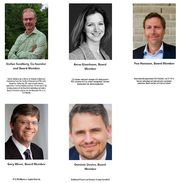
AlixLabs Board of directors: https://www.alixlabs.com/who-we-are

* Atomic Layer Etch Pitch Splitting (APS). As previously reported (April 30th, 2021) The US Patent Office has approved AlixLabs’s patent application for nanofabrication by ALE Pitch Splitting (APS). The US Patent Office has issued a patent (US10930515) on February 23, 2021. The patent covers methods to split nanostructures in half by a single process step using Atomic Layer Etching (ALE). The method has the potential to have a big impact on the semiconductor industry by enabling sustainable scaling of electronic components and shrink chip designs further in a cost-effective way. The method is complementary for single exposure Immersion and Extreme UV (EUV) Lithography and corresponding multiple patterning technologies like self-aligned double and quadruple patterning (SADP resp. SAQP) as well as multiple exposure lithography-etch and directed self-assembly (DSA).

Jonas Sundqvist, CEO of AlixLabs, phone +46 767 63 94 67, email jonas@alixlabs.com

AlixLabs (www.alixlab.com) is an innovative startup founded in 2019 in Lund, Sweden, enabling the semiconductor industry to scale down Logic and Memory components in a cost-effective manner by the use of ALE Pitch Splitting (APS).

Saturday, February 27, 2021

2021 ISSCC - Plenary Session with Dr. Mark Liu, TSMC Chairman

TSMC recently delivered a plenary session at ISSCC 2021. by Dr. Mark Liu, TSMC Chairman. He gave a vision and path of how semiconductor technologies will continue to innovate over the coming years and decades. Below you can watch the Dr. Liu’s plenary session.

Abstract: The foundry business model, pioneered by TSMC more than three decades ago, brought a sea change to technology innovation and how integrated circuits (ICs) and systems are designed and manufactured. Access to semiconductor technology is no longer limited to large corporations that invest billions of dollars to build a fabrication plant. The foundry model has democratized IC innovation, making it available to all visionaries and innovators.

Today, an open innovation platform that connects innovators with semiconductor-technology providers is a vital link in the global supply chain. Our industry has already begun to look beyond just engineering individual chips manufactured on wafers, and have moved to integrate individual chips into systems. System performance and energy efficiency will continue to advance at historical rates, driven by innovations from many aspects, including materials, device and integration technology, circuit design, architecture, and systems. User applications drives design choices, and design choices are enabled by technology advancements. Advances in an open innovation ecosystem will further lower the entry barriers and unleash the future of innovation.


Friday, February 12, 2021

SIA Webinar: A Review of the 2020 Semiconductor Market and a Look to 2021

2020 proved to be one of the more unique years in recent times in terms of semiconductor market performance. Pre-2020 market forecasts were quickly and fundamentally rethought at the start of the year, as the COVID-19 pandemic upended the world. Significant uncertainly on how semiconductor sales would react to the pandemic existed for much of the year, especially during the first half. As monthly World Semiconductor Trade Statistics sales figures rolled in through the latter half of 2020, it became clear 2020 sales would end up better than most had initially feared.

Please join a panel of semiconductor market experts to help us make sense of the trends that shaped the semiconductor market in 2020 and look ahead to what the market has in store for 2021. Panelists include: Andrea Lati, Vice President, Market Research at VLSI Research; Dale Ford, Chief Analyst at the Electronic Components Industry Association (ECIA); and C.J. Muse, Senior Managing Director, Head of Global Semiconductor Research at Evercore ISI. The session will be moderated by Falan Yinug, Director of Industry Statistics and Economy Policy at SIA.
Presentations:

Andrea Lati, VLSI Research


Tuesday, January 12, 2021

Semiconductor Materials $50B Market on a Strong Run in 2021

Semiconductor Materials $50B Market on a Strong Run in 2021Pandemic pushing people to Work From Home and School From Home

San Diego, CA, January 12, 2021: TECHCET announced that global revenues for semiconductor manufacturing and packaging materials grew approximately 4% year-over-year (YoY) in 2020 to ~US$50B, and are expected to grow ~7% in 2021 to nearly US$54B. The COVID-19 pandemic has created strong demand for both logic and memory ICs to support Work From Home (WFH) and School From Home (SFH), and such demand is expected to increase despite expanding availability of virus vaccines. Also, demand for automotive ICs has recovered and will be an important driver in 2021 growth. The compound annual growth rate (CAGR) through 2024 is forecast at 5.3% as per the latest TECHCET Critical Materials Reports (CMR) and shown in the attached figure.

Analysts' Alerts emailed to CMR purchasers help them anticipate and mitigate potential supply-chain disruptions. Excerpts have been publicly disclosed on the following critical materials (https://lnkd.in/dzAZcCw):

* IPA in "CMC Considers Bio-Solvents to Reduce Fab Risks",
* HF in "Semi Wet Chemicals US$2B Market Threatened by Localization", and
* Lanthanum in "Rare Earth Elements (REE) Supply Uncertain for IC Fabs".