Showing posts with label Intel. Show all posts

Saturday, December 14, 2019

IEDM 2019 News - Intel roadmap to 1.4 nm by 2029

Limitless - Intel disclosed its extended roadmap to 1.4 nm process node by 2029 including back porting: One of the interesting disclosures at the IEEE International Electron Devices Meeting (IEDM) was that Intel expects to be on 2 year cadence with its manufacturing process node technology, starting with 10nm in 2019 and moving to 7 nm EUV in 2021, then 5 nm in 2023, 3 nm in 2025, 2 nm in 2027, and 1.4 nm in 2029. 
 
In between each process node, as Intel has stated before, there will be iterative + and ++ versions of each in order to extract performance from each process node. The only exception to this is 10nm, which is already on 10+, so we will see 10++ and 10+++ in 2020 and 2021 respectively. The interesting element is the mention of back porting. This is the ability for a chip to be designed with one process node in mind, but perhaps due to delays, can be remade on an older ‘++’ version of a process node in the same timeframe.

 
Intel's slide with ASML's animations overlayed, as shown in the slide deck distributed by ASML. Note by Anandtech: "After some emailing back and forth, we can confirm that the slide that Intel's partner ASML presented at the IEDM conference is actually an altered version of what Intel presented for the September 2019 source. ASML added animations to the slide such that the bottom row of dates correspond to specific nodes, however at the time we didn't spot these animations (neither did it seem did the rest of the press). It should be noted that the correlation that ASML made to exact node names isn't so much a stretch of the imagination to piece together, however it has been requested that we also add the original Intel slide to provide context to what Intel is saying compared to what was presented by ASML. Some of the wording in the article has changed to reflect this. Our analysis is still relevant." Please see the full article in Anandtech for all the details: LINK
 
----------
By Abhishekkumar Thakur

Thursday, October 17, 2019

Intel Oregon is looking for young CVD, ALD and PVD experts

[Intel, Hillsboro Oregon, USA] We are hiring Ph.D. candidates or recently received a Ph.D. degree in the metals thin-film area. We are giving priorities to the candidates who have exceptional backgrounds in physical vapor deposition (PVD), chemical vapor deposition (CVD), atomic layer deposition (ALD), and/or Electrodeposition fields. Strong plasma physics and vacuum science knowledge will be needed for PVD, CVD, and ALD deposition area candidates. 
 
 
 Intels Fab D1X in Oregon USA (Intel.com)
 
We are also looking for candidates with synthetic chemistry backgrounds for CVD/MOCVD (metal-organic chemical vapor deposition) precursor development. In the Electrodeposition area, we are looking for candidates with a strong background in electrochemistry, plating related thin film deposition.

Generic Job description can be found here - https://jobs.intel.com/ListJobs/ByKeyword/JR0099326/

Please send me your resume directly to shaestagir.chowdhury@intel.com
 
------------
Guest Blog by Dr. Shaestagir Chowdhury, Principal Engineer at Intel Corporation, Hillsboro, Oregon
 

Monday, September 23, 2019

Intel at EECS Colloquium "Moore’s Law Is Not Dead"

Intel’s Jim Keller: “We’re all building nanowires… Intel, TSMC, Samsung” Keller in his "Moore’s Law Is Not Dead" talk at UC Berkeley this week said, “We had planar transistors, we went to FinFET. We’re all building nanowires in the fab. Intel, TSMC, Samsung, everybody’s working on it. There’s a really interesting thing. While the world thinks Moore’s Law’s dead, the fabs and the technologists think it’s not and everybody’s announced now a 10-year roadmap for Moore’s Law.” 


The UC Berkeley EECS Events team has live streamed the entire talk over on YouTube and you can catch up on this fascinating, intimate little talk (below).
 
 ----------
By Abhishekkumar Thakur

Sunday, May 12, 2019

Intel 2019 Investor Meeting: 7 nm Product in 2021

Intel held its 2019 investor meeting May 8, 2019 (LINK), it's first since 2017, and CEO Bob Swan announced that Intel would launch its 7 nm process in 2021 to challenge TSMC's 5 nm products.

Intel's Xe graphics will be the leading 7 nm product, which will come on the heels of Intel's first discrete 10 nm GPU that arrives in 2020. The company also unveiled its first block diagram of the Ice Lake architecture and announced that its new 10nm Tiger Lake processors will come to market in 2020.
Source: Tom´s Hardware LINK

 (intel.com)

----------
By Abhishekkumar Thakur

Thursday, January 3, 2019

Innovation and IP filing in Atomic Layer Deposition has moved from Memory to Logic

By studying the filing of IP world wide one can clearly see the trend how innovation in Atomic Layer Deposition (ALD) has moved from Memory to Logic. During the introduction of ALD (2003 to 2006) in high volume manufacturing of DRAM on 300 mm wafers most IP was filed by Samsung, Micron and SK Hynix. 10 years later (2013-2018) the IP filing lead has been taken over by Logic MPU manufacturers TSMC, Intel and Globalfoundries.

The patent application assignee from the past 25 years.

Tuesday, December 25, 2018

Intel 10 nm Logic Process Analysis (Cannon Lake) by TechInsight

[TechInsight, LINK] TechInsights has found the long-awaited Cannon Lake - the Intel 10 nm logic process inside the i3-8121U CPU, used in the Lenovo IdeaPad330.

 
This innovation boasts the following:

  • Logic transistor density of 100.8 mega transistors per mm2, increasing 10nm density 2.7X over the 14nm node
  • Utilizes third generation FinFET technology
  • Minimum gate pitch of Intel’s 10 nm process shrinks from 70 nm to 54 nm
  • Minimum metal pitch shrinks from 52 nm to 36 nm
Process Highlights:

  • Deepest scaled pitches of current 10 nm and upcoming 7 nm technologies
  • First Co metallization and Ru usage in BEOL
  • New self-aligned patterning schemes at contact and BEOL
Design Highlights:

  • Hyperscaling via 6.2-Track high density library
  • Contact on active gate (COAG) cell-level usage
---------
By Abhishekkumar Thakur

Friday, June 15, 2018

Cobalt and Ruthnium confirmed in Intel 10nm Cannon Lake BEOL

TechInsights has found the long-awaited Cannon Lake - the Intel 10 nm logic process inside the i3-8121U CPU, used in the Lenovo IdeaPad330.
 
This innovation boasts the following:

  • Logic transistor density of 100.8 mega transistors per mm2, increasing 10nm density 2.7X over the 14nm node
  • Utilizes third generation FinFET technology
  • Minimum gate pitch of Intel’s 10 nm process shrinks from 70 nm to 54 nm
  • Minimum metal pitch shrinks from 52 nm to 36 nm
Process Highlights:

  • Deepest scaled pitches of current 10 nm and upcoming 7 nm technologies
  • First Co metallization and Ru usage in BEOL
  • New self-aligned patterning schemes at contact and BEOL
Source: TechInsight (LINK)

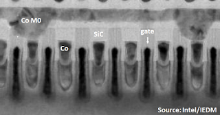
By reading this it is not possible to determine exactly how Ruthenium is used or how it has been deposited and there are several options like barrier and seed layer for plating Copper or Cobalt. What is known is that Intel presented already at IEDM2017 the use of cobalt in their 10 nm MOL/BEOL process flow as contacts and M0/M1 lines as well as barrier/seed for copper and copper cap for complete encapsulation of copper up to M5.


Intel 10nm mid end of line cobalt and copper metallization as presented at IEDM 2017.

Friday, April 27, 2018

Intel shifts high volume 10 nm shipments to 2019 due to yield issues from multi-patterning

As reported by Reuters [LINK], Intel bet the earnings expectations for the first quarter driven by the biggest-ever quarterly jump in its data centre business and small-but-steady growth in its personal computer business.However, Intel also announced that they are pushing out volume production of their 10 nm Logic process to 2019, which was most recently announced for the 2nd half of 2018. during the 1Q 2018 earnings conference calls more details were given:

[Seeking Alpha, LINK] "We continue to make progress on our 10-nanometer process. We are shipping in low volume and yields are improving, but the rate of improvement is slower than we anticipated. As a result, volume production is moving from the second half of 2018 into 2019. We understand the yield issues and have defined improvements for them, but they will take time to implement and qualify. We have leadership products on the roadmap that continue to take advantage of 14-nanometer, with Whiskey Lake for clients and Cascade Lake for the data center coming later this year.

Moore's Law is essential to our strategy and our product leadership. It continues to create significant value for Intel and our customers. While it's taking longer and costing more to deliver and yield advanced process technologies, we are able to optimize our process and products within the node to deliver meaningful performance improvements.

For example, 14-nanometer process optimizations and architectural improvements have resulted in performance gains of more than 70% since the first 14-nanometer products were launched. We combine these advances in manufacturing technology and architecture to produce truly leadership products. And it's that product leadership that ultimately matters most to our customers and end users."

Brian M. Krzanich - Intel Corp.

Earnings call slides [Seeking Alpha, LINK]

In the Q&A Mr. Krzanich elaborated on the reason behind the 10 nm push out and he explained how it is mainly due to yield issues coming from multiple patterning (SADP and SAQP):

- Intel have 10 nm product and process leadership and are shipping 10 nm products today. 
- Those are the densest, highest performing products out there.
- Intel is slowing the ramp down to fix yield issues related to patterning.
- In multi-multi-patterning (SAQP) there are six layers of patterning to produce a feature. 
- Intel understand the yield issues, which are tied to 10 nm being the last technology tied to not using EUV and the amount of multi-patterning and the effects of that on defects.


Intel’s 10 nm Platform Process was presented in detail at the IEDM 2017 (Dec 2017) “A 10nm High Performance and Low-Power CMOS Technology Featuring 3rd Generation FinFET Transistors, Self-Aligned Quad Patterning, Contact over Active Gate and Cobalt Local Interconnects” and you may study the details in this excellent article by Dick James [Solid State Technology, LINK]

Media coverage:
 
The Register
 

Sunday, October 22, 2017

Intel to present 10 nm Logic with 3rd gen FinFET and 2 level Cobalt interconnect

IEDM 2017 Announcement (LINK, Press kit): Intel researchers will present a 10nm logic technology platform with excellent transistor and interconnect performance and aggressive design-rule scaling. They demonstrated its versatility by building a 204Mb SRAM having three different types of memory cells: a high-density 0.0312µm2 cell, a low voltage 0.0367µm2 cell, and a high-performance 0.0441µm2 cell. The platform features 3rd-generation FinFETs fabricated with self-aligned quadruple patterning (SAQP) for critical layers, leading to a 7nm fin width at a 34nm pitch, and a 46nm fin height; a 5th-generation high-k metal gate; and 7th-generation strained silicon. There are 12 metal layers of interconnect, with cobalt wires in the lowest two layers that yield a 5-10x improvement in electromigration and a 2x reduction in via resistance. NMOS and PMOS current is 71% and 35% greater, respectively, compared to 14nm FinFET transistors. Metal stacks with four or six workfunctions enable operation at different threshold voltages, and novel self-aligned gate contacts over active gates are employed.

The graph on the left shows that the new platform maintains traditional scaling trends, while the photomicrograph on the right shows the platform’s 12-layer interconnect stack.


Reference: Paper 29.1, “A 10nm High Performance and Low-Power CMOS Technology Featuring 3rd-Generation FinFET Transistors, Self-Aligned Quad Patterning, Contact Over Active Gate and Cobalt Local Interconnects,” C. Auth et al, Intel

2017 IEEE International Electron Devices Meeting
December 2-6, 2017
Hilton San Francisco Union Square
333 O’Farrell Street
San Francisco, CA 94102

Wednesday, March 29, 2017

Intel announce first SAQP in Logic and Much Moore at 10 nm

Intel announce first SAQP and Much Moore at 10 nm during their most recent Investor Show (March 28, 2017). SAQP is already process of record in DRAM at Sasmung since 2016 10 nm class DRAM was introduced (LINK)


Technology Manufacturing Day - Strategy Overview (Stacy Smith)


Technology Manufacturing Day - Moore’s Law (Mark Bohr)

Technology Manufacturing Day - 14nm Leadership (Ruth Brain)


Technology Manufacturing Day - 10nm Leadership (Kaizad Mistry)


[check out slide 13, screendump]


Technology Manufacturing Day - 22FFL (Mark Bohr)


Technology Manufacturing Day - IDM Advantage (Murthy Renduchintala)


All recent briefings: LINK