Showing posts with label ALD Equipment. Show all posts

Tuesday, June 6, 2023

TNO heads consortium developing ‘Third-generation electrolyzers with SparkNano ALD technology

Dutch research center TNO, along with three technical universities and several enterprises, is leading a consortium to develop "Third-generation electrolyzers," aiming to create more affordable and efficient electrolyzers for hydrogen production. 

The collaboration will focus on designing advanced stacks and components for electrolysers, as well as exploring manufacturing technologies. The goal is to establish a significant presence in the global electrolyser market. The five-year project will investigate various methods of water splitting and CO2 electrolysis, with the expectation that different concepts will synergize and contribute to the development of cutting-edge production technology. 


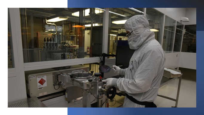
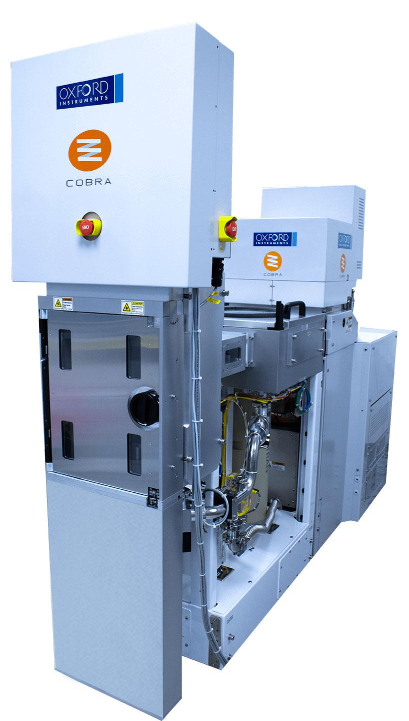
TNO's Atomic Layer Deposition technology, marketed by SparkNano, holds promise for creating novel electrolysers. The initiative is part of NXTGEN HIGHTECH, which aims to provide innovative solutions in key areas of production technology. Participating companies, knowledge institutions, and groups include Admatec, Bosch Transmission Technology, Coval Energy, Delft University of Technology, Eindhoven University of Technology, Magneto Special Anodes, and others.

Links &sources:

TNO heads consortium developing 'Third-generation electrolyzers' - (industryandenergy.eu)

News | P2Hydrogen - VoltaChem

Home - NXTGEN Hightech

SparkNano | Spatial Atomic Layer Deposition (ALD) technology (spark-nano.com)

Friday, June 2, 2023

ASM breaks ground on new state-of-the-art innovation and manufacturing center in Hwaseong, Korea

ASM International N.V. is embarking on the construction of a state-of-the-art innovation and manufacturing center in Hwaseong, South Korea. With a groundbreaking ceremony to be held soon, the expansion project is part of ASM's US$100 million investment plan and follows a Memorandum of Understanding signed with the Ministry of Trade, Industry and Energy of South Korea. The investment aims to bolster ASM's research and product development infrastructure and increase manufacturing capacity to meet the growing demand for semiconductors. The company also intends to create job opportunities in engineering, R&D, and manufacturing, contributing to workforce development in Korea.


The ceremony will be attended by ASM's CEO, Benjamin Loh, and other dignitaries, including political figures and business partners. Loh expressed his enthusiasm for the expansion in Hwaseong, highlighting the potential and dedication of the Korean people. The investment signifies ASM's commitment to Korea and its ambition to grow the business while enabling the development of advanced technologies in the semiconductor industry. Hwaseong has played a vital role in ASM's growth, serving as a hub for advanced R&D and technology for both local and global customers.

The existing Hwaseong facility, which currently employs over 450 people, will be expanded to accommodate more employees as the company continues to grow. The new extension will add 31,000 m2 across eight floors, more than doubling the facility's R&D area and nearly tripling its manufacturing area. YK Kim, Chairman of ASM Korea, emphasized that the expansion is an investment in people and the semiconductor ecosystem in Korea, aiming to support the country's semiconductor industry growth in collaboration with the government, customers, and suppliers.

ASM's commitment to Hwaseong demonstrates its dedication to the Korean market and its goal of facilitating domestic semiconductor innovation while meeting global customer demands. The company's local R&D team has been instrumental in developing groundbreaking technologies in the industry, such as ALD QCM quad chamber modules, TENZA™ ALD for high aspect ratio gap-fill, and high-quality PEALD silicon and metal oxides and nitrides for various applications. 

Release of TENZA(TM): BALD Engineering - Born in Finland, Born to ALD: ASM International launches TENZA ALD Quad Chambers for silicon oxide gap-fill and liners on the XP8 platform


ASM Korea MOU: BALD Engineering - Born in Finland, Born to ALD: Dutch ALD euipment leader ASM to invest $100 mil. in Korea for facility expansion


Finnish ALD equipment manufacturer Beneq has entered a partnership with Lung Pien Vacuum Industry Co., Ltd. in Taiwan.

Finnish ALD equipment manufacturer Beneq has partnered with Taiwan's Lung Pien Vacuum Industry to promote ALD technology for optical applications. They held a seminar to exchange knowledge and explore ALD solutions for mass production challenges. ALD is a process that deposits atomic thin films with advantages like large-area coverage and precise film thickness control. Beneq, a global leader in ALD equipment, introduced AtomGrassTM ALD, a wide-angle broadband anti-reflective coating. Lung Pien will provide Beneq's equipment and services to its optics customers in the Asia-Pacific region. The partnership aims to actively promote ALD coating technology for high-end curved lenses in Taiwan's optical market.

Finnish ALD equipment manufacturer Beneq has formed a partnership with Lung Pien Vacuum Industry, a prominent vacuum coating equipment manufacturer based in Taiwan. The collaboration aims to promote ALD technology for emerging optical applications, such as camera lenses for mobile phones and automobiles. In April, the two companies organized an "ALD Optical Coating" seminar in Taiwan, inviting major optical manufacturers to exchange knowledge and explore ALD solutions for mass production challenges. ALD is a deposition process that involves the formation of self-limited reactions between precursor gases and a substrate surface, resulting in atomic thin films with advantages like large-area coverage, high step coverage, low-temperature processing, and precise film thickness control.


Peter Hsieh (left standing), Beneq’s Advanced ALD Sales Director, and Kalle Niiranen (right standing), Technical Sales Manager, hosting the ALD Optical Coating seminar on the 20th of April in Taichung, Taiwan.

Beneq has been a pioneer in industrial ALD production since 1984 and has established itself as a global leader in ALD equipment manufacturing. The company offers a wide range of technical products and R&D services, with a focus on finding industrial ALD solutions through collaboration and co-development. Beneq recently introduced AtomGrassTM ALD, an innovative wide-angle broadband anti-reflective (AR) coating. This solution provides exceptional anti-reflective properties with less than 0.07% average reflectance across a wide wavelength range and significantly improves performance at high angles of incidence.

According to Peter Hsieh, Sales Director of Beneq's Advanced ALD Business Unit, the demand for ALD is increasing in the nano-processes of the integrated circuit industry. ALD has replaced traditional methods like CVD and PVD for many key thin-film processes. Hsieh believes that ALD's development is now closer to industrial-grade 12-inch mass production equipment, opening up excellent application opportunities in various fields, including optoelectronics, automotive, medical materials, and more.

Lung Pien Vacuum Industry, founded in 1991, has a longstanding relationship with the optical industry. The company offers a comprehensive range of services, including product design, development, equipment manufacturing, production planning, operator training, and process design consulting. While Lung Pien primarily focuses on vacuum evaporation and sputtering equipment manufacturing, thin film process technology services, and other related products, their partnership with Beneq will enable them to provide Beneq's ALD equipment and services to their extensive network of optics customers in the Asia-Pacific region. The collaboration between Beneq and Lung Pien aims to actively promote ALD coating technology for high-end curved lenses in Taiwan's optical market, leveraging ALD's ability to provide uniform conformal thin film layers for complex structures.

Wednesday, May 3, 2023

Forge Nano Partners with Aleon Renewable Metals for Battery Recycling and Supply of ALD Materials for EV Batteries

DENVER , May 2, 2023 /PRNewswire/ -- Forge Nano, a global leader in surface engineering and precision nano-coating technology, and Aleon Renewable Metals (ARM), an integrated lithium-ion battery recycler, announced a partnership today for battery recycling and supply of battery materials. Aleon Renewable Metals will recycle Forge Nano's battery scrap at its industry-leading battery recycling facilities in Texas and Oklahoma utilizing Forge Nano's technology to manufacture cathode active materials (CAM) from the battery grade materials produced by ARM. These facilities aim to make battery recycling easier and more cost effective while outputting leading CAMs made in the U.S. using Forge Nano's proprietary Atomic Layer Deposition (ALD) coating technology, Atomic Armor™. Batteries made with Atomic Armor are optimized to be longer-lasting and safer than current batteries on the market. ARM's facility is expected to annually produce battery grade materials equivalent to 35 GWh of renewable power.


Approximately three billion batteries are thrown away every year in America alone, posing environmental and economical threats far beyond the lifetime of the battery itself. Until now, few companies have addressed the challenges of recycling lithium-ion battery materials. Together, Forge Nano and Aleon are bringing over four decades of combined experience aiming to make E-waste a thing of the past with a 100% renewable energy process.

"In partnership with Aleon Renewable Metals, our technology will be used to provide sustainable and significant cost and performance advantages over competing recyclers making CAMs," said James Trevey , CTO, Forge Nano. "With the cost and performance benefits enabled by Atomic Armor, implementation of this U.S.-born nano-coating technology into the battery-recycling loop embodies the leapfrog improvement in technological advancement everyone has been waiting for in the lithium-ion battery industry."

"We are dedicated to driving sustainability and innovation. Aleon Renewable Metals leverages our proprietary recycling technologies to support the global transition to circular supply chains and cleaner energy. Our high-purity, cost-competitive battery grade materials are positioned to meet the growing domestic demands of the EV market for metal sulfates and lithium compounds used in high-performance cathodes," said Tarun Bhatt , CEO of Aleon Renewable Metals. "With our experience in metal recovery and commitment to sustainable solutions, we are excited to partner with Forge Nano to develop downstream cathode active materials. Together, we will address the projected lithium, nickel, and cobalt supply/demand deficits to create a more attractive environment for sustainable energy production."

As active members of NAATBatt and the MPSC , both companies have demonstrated their dedication to a sustainable battery ecosystem, and their commitment to making a difference in the battery waste problem. This exciting partnership will bring together two world-renowned battery powerhouses in the hopes of taking battery recycling technology to the next level.

"Particle coatings in the field of battery technology are an enabler to excel in the marketplace, which Forge Nano is doing as the global leader in ALD methods to achieve the essential coating characteristics," said Bob Galyen , energy storage technology expert and chairman of Galyen Energy. "The U.S. battery supply chain depends on this kind of innovation to compete on the world stage."

Monday, April 24, 2023

Oxford Instruments to supply KAUST with hardware upgrades and ALE systems

Significant partnership with KAUST: hardware upgrade and support its cutting-edge ALD research with the addition of ALE capability

Oxford Instruments Plasma Technology has announced a significant agreement with the Saudi Arabia-based King Abdullah University of Science and Technology (KAUST) Core Labs, a system of multidisciplinary and interconnected research laboratories. Under the agreement, KAUST’s Core Labs and Research Infrastructure benefits from the addition of two Oxford Instruments PlasmaPro®100 Cobra® atomic layer etch (ALE) systems to add to its existing Oxford Instruments FlexAL® atomic layer deposition (ALD) capability. 

With both ALE and ALD modules, KAUST is now even better positioned to develop its world-leading technology research and bridge the gap between academia and industry, by enhancing projects like their cutting edge research on Oxford Instruments ALD equipment GaN HEMT Origin of Interfacial Charges and GaN HEMT Highly Suppressed Interface Traps.


Monday, April 10, 2023

Korea’s Jusung Engineering set to supply non-memory chip gears overseas

South Korean chip equipment manufacturer Jusung Engineering Co. is set to supply atomic layer deposition (ALD) equipment to a leading global chip manufacturer for system chips at a U.S. integrated device manufacturer and a major foundry in Taiwan, according to its Chairman and Chief Executive Officer Hwang Chul-joo.

“The test conducted by our global customer on the Guidance Series, an ALD equipment developed for the first time in the world in 2020, has been completed and we expect the purchase order to come in the first half of this year,” Hwang told Maeil Business Newspaper.

In general, it takes two to three years for a chip equipment to be verified and applied to mass production after development. Jusung Engineering, which has been engaged in the joint development of an ALD equipment with a global non-memory chip manufacturer since 2015, has carried out tests with multiple clients from 2020.

Jusung Engineering until now had been focused on the manufacturing deposition equipment that coats necessary substances to wafers as part of a chip manufacturing process.


Monday, December 19, 2022

Thin layers paved the way for ASMI’s success - Outgoing CTO Ivo Raaijmakers explains what atomic layer deposition has brought the semiconductor industry

ASM International played a key role in developing a deposition technique that has saved Moore’s law more than once. Outgoing CTO Ivo Raaijmakers explains what atomic layer deposition has brought the semiconductor industry – and ASMI – and what more is in store.
This vision has come true. The technique that ASMI acquired through Microchemistry – atomic layer deposition (ALD) – has become an integral part of the semiconductor manufacturing process. And that’s just the beginning, according to Raaijmakers. The demands placed on material layers are ever higher – thinner, more uniform, featuring just the right properties – and ALD is the best technique to meet them, the former CTO argues.


Well before ALD had proven itself in the deposition of high-k materials, Raaijmakers was already looking at which applications would follow. On his initiative, ASMI acquired Korean company Genitech in 2004, a specialist in plasma-enhanced ALD technology (PEALD). Plasmas are more reactive than un-ionized gases and therefore can deposit materials at lower temperatures. Because chipmakers often have to deal with strict temperature budgets, PEALD expands the scope of ALD.

Saturday, December 17, 2022

Kokusai Electric relies on patterned 3D substrates in thin film process metrology from Chipmetrics

Kokusai Electric is one of the leading semiconductor thin film process equipment manufacturers in the world. Recently, in the context of Japan Society of Applied Physics 69th Spring Meeting 2022, Kokusai presented their advanced thin film measurement and analysis concept used in their semiconductor process development.

The concept focuses on film thickness and localized film composition measurements from the special designed 3D patterned substrates, where the patterns are fine high aspect ratio structures.

The average film thickness is obtained indirectly by measuring the mass change in the special 3D patterned wafer before and after the film depositions. The thickness accuracy is further improved by taking into account the high aspect ratio and wafer level non-uniformity measured by PillarHall® Lateral High Aspect Ratio (LHAR) test chips positioned on the carrier wafer. The PillarHall® measurement, enables easy screening after peeling off the top roof membrane and by measuring the film thickness distribution and conformality by the ellipsometer line-scanning measurements.

PillarHall® LHAR test chip has also another important function in Kokusai’s analysis concept. Namely, it is used for film elemental composition characterization along the trench wall in high aspect ratio structure. The measurement is carried out as a line-scan by XPS or SEM-EDS. For example, the characterization showed that two kinds of SiN processes behaved differently and Si/N composition changes along the high aspect ratio (AR>1000) trench were observed.


Figure 1. PillarHall experiment summary


Figure 2. SiN film thickness data


Figure 3. SiN(2) XPS data

Figures 1-3 show the PillarHall experimental set-up, data from the film thickness penetration depth profiles and XPS composition data of two kind of Kokusai’s SiN processes, SiN (1) and SiN (2).

Kenji Kameda and Akane Kitamura from Metrology Team, Kokusai Electric emphasized that:” It is difficult to obtain the analysis of thin films on high aspect ratio patterns without cross-sectional TEM. PillarHall is a simple and effective tool, it has fine patterns, and it enables us to use XPS and ellipsometer instead of TEM. Therefore, PillarHall is useful as an efficient measurement tool to improve Kokusai’s film forming technology.”

PillarHall LHAR test chip is a product of Chipmetrics Ltd, Finland. Chipmetrics CEO Dr. Mikko Utriainen reminds that any PillarHall data can be published without confidentiality concerns and the results are also well comparable between reactor systems and processes. The openness and accuracy of the ALD conformality data was one of the reasons why pioneering ALD scientists in Finland started to develop the PillarHall concept already in 2013.

Kokusai’s example shows that PillarHall is an efficient measurement tool and help to improve film forming technology for advanced semiconductor processes.

PillarHall is a product of Chipmetrics Ltd. Contact: info@chipmetrics, www.chipmetrics.com

Friday, December 16, 2022

MIT.nano adds new instruments to create and analyze at the nanoscale from Arradiance

The Arradiance GEMStar XT-DP plasma-enhanced atomic layer deposition (ALD) system was installed at MIT.nano in May.


The system is dedicated specifically to deposit high-quality nanometer-scale thin oxide films including aluminum oxide, hafnium oxide, zirconium dioxide, and silicon dioxide. The Arradiance ALD can be used for samples ranging from small pieces up to 200-mm wafers and has a load lock that isolates the deposition chamber from the user, allowing for better contamination control.


Friday, November 25, 2022

Applied Materials Delivers Strong FY 2022 Numbers including Picosun ALD

Semiconductor equipment maker Applied Materials has reported strong earnings for FY 2022 (ended October 30). Total sales revenue increased 12% YoY to $25.78 billion despite supply chain shortages, geopolitical and macroeconomic headwinds, and softening consumer demand.

LINK: https://ir.appliedmaterials.com/

The company’s uniquely enabling technology and growing installed base will be its key growth drivers as chipmakers accelerate ramping up of new process nodes in R&D for high-volume manufacturing.


Key developments in FY 2022
  • Applied Materials acquired Picosun, a Finland-based innovator in atomic layer deposition (ALD) technology. This acquisition broadens Applied’s product portfolio and puts it in a great position to capture a large portion of the specialty semiconductor market in the coming years.
  • Collaboration with the Institute of Microelectronics (IME), a research institute under Singapore’s Agency for Science, Technology and Research (A*STAR). IME’s strategic R&D capabilities complement well Applied’s expertise in advanced packaging solutions and will accelerate material, equipment and process technology solutions for hybrid bonding and other emerging, 3D chip integration technologies.
  • Introduced new Ioniq™ PVD system to solve wiring resistance challenges of 2D scaling. This new integrated solution offers a significant reduction in electrical resistance, which has become a critical bottleneck to further improvements in chip performance and power.
Financial highlights
  • Semiconductor Systems revenue increased 15% YoY in FY 2022 to $18,797 million on account of strong orders as customers continued to invest in next-generation technology.
  • Applied Materials’ service revenue increased 11% YoY in FY 2022 to $5,543 million, accounting for 21% of the annual net revenue.
  • Display and Adjacent Markets revenue decreased 19% YoY in FY 2022 to $ 1,331 million.
  • Non-GAAP gross margin was at 46.6% in FY 2022.
  • Non-GAAP operating profit grew by over 7% to $7.86 billion.
  • Non-GAAP EPS increased nearly 13% to $7.70.
  • Total ending backlog increased 62% to $19 billion with Semiconductor Systems backlog increasing 90% to nearly $12.7 billion and services backlog increasing 30% to over $5.6 billion.
  • The company generated about $5.4 billion in operating cash flow and over $4.6 billion in free cash flow.
  • The company’s installed base grew 8% YoY in FY 2022.
  • The number of tools under comprehensive, long-term service contracts grew 16% YoY with the over 90% renewal rate for these agreements demonstrating the value customers see in subscription services.
  • New export regulations for US semiconductor technology sold in China reduced Semiconductor Systems and AGS fourth quarter revenue by approximately $280 million.

Monday, October 10, 2022

Samco launches new ICP Tornado Plasma ALD system

Samco, a leading manufacturer of etching, deposition and surface treatment processing equipment for the semiconductor and related industries and academic facilities, launches the new Plasma Enhanced Atomic Layer Deposition (PEALD) system, "AD-800LP". The main target of the system is gate oxide film deposition for next-generation power devices of silicon carbide (SiC) and gallium nitride (GaN) materials, which will play important role toward carbon neutral.


Tornado ICP Coil®,  Samco ICP etch systems are equipped with Tornado ICP Coil® which was specially designed for compound semiconductor etching. It is difficult to achieve desired profiles of InP and GaAs due to byproduct redeposition. The Tornado ICP Coil® reduces byproduct redeposition by optimizing etchant species and densities in plasma etching. (Source: Samco)

The plasma enhanced ALD system "AD-800LP" is a multi-purpose R&D system equipped with a unique ICP plasma source called "Tornado ICP", in addition to the conventional thermal ALD capability. AD-800LP enables various film deposition such as oxide or nitride films by Tornado ICP, which is Samco's proprietary plasma technology and is different from remote plasma. Tornado ICP enables stable plasma discharge even in the high-pressure range during ALD deposition.

“We are also considering a cluster ALD system that can connect multiple reaction chambers for production” says Tsukasa Kawabe, President and COO of Samco. “The launch of the AD-800LP will greatly enhance our presence in the world ALD equipment market.” Tsukasa adds.

As a global mid-sized company, Samco has successfully delivered numerous dry etch systems and plasma enhanced CVD systems for the electronic device field, mainly for compound semiconductors such as SiC, GaN, and GaAs, not only in Japan but also in the United States, Europe, Taiwan, Korea, China, Southeast Asia, India, and other countries.

The new Research Center for Nano Thin Films & Materials, which opened in February 2022, conducts research and development of unique thin film deposition, including ALD system. Samco will continue to utilize our "thin-film technology" to develop unique products and expand sales globally.

About Samco Inc.
Samco Inc. (TSE: 6387) stands for Semiconductor And Materials Company, and is a leading manufacturer of processing equipment for the semiconductor and related industries founded by Mr. Osamu Tsuji in Kyoto, Japan in 1979. Over the past forty-three years, more than 4,300 Samco systems have been installed and used in 35 different countries. Its equipment and thin film technology are widely adopted in the fabrication of semiconductor devices, including BAW filters, SiC power devices, GaN RF devices, GaAs VCSELs, InP lasers, microLEDs, MEMS, TSVs, advanced packaging, and so on. Learn more at https://www.samcointl.com/.

NCD’s ALD technology and equipment for oxidation barrier of copper-based substrates

Copper is a metal used widely as the main material of Printed Circuit Board (PCB) and Lead Frame. But it is required to protect the oxidation because copper is easily oxidized in the condition of humidity, temperature, and pH, etc.

Electroless Nickel Immersion Gold (ENIG), Organic Solderability Preservative (OSP), Immersion Sn or Ag (ImSn or ImAg) is generally used to prevent oxidation of opened copper area after Solder Masking in PCBs. The lead Frame is protected from oxidizing by plating Au, Ag, Pd, and Ni after Lead Frame forming.

Recently, many groups have studied about preventing oxidation on the surface of copper by various corrosion protection layers of ALD metal oxides. Especially, Appling Al2O3 layer to the oxidation barrier is actively being researched.


 < Surface images and TEM & EDS of Cu plates coated by ALD thin films after annealing test >

After depositing Al2O3 layers on Cu-plated plates with various film thicknesses and process temperatures, the oxidation and corrosion behavior of the coated copper was examined with different annealing times in the oven. There was no oxidation before annealing, but after annealing for 1hr, as the sample’s thickness lowered and process temperature decreased, the oxidation happened and increased gradually. There was no oxidation on the plates coated with 50~60 ALD cycles and at process temperatures of 70~100 after annealing for 5hr, and oxidation didn’t occur only in the case of 60 cycles and 100 after annealing for 24hr.

To analyze the change of the structure and confirm the oxidation behavior, TEM and EDS were measured on 5 and 10nm Al2O3 coated Cu plates at 100. The results showed that a thick Cu oxide layer was built by combining Cu coming out through the 5nm Al2O3 layer and outer oxygen after annealing.

On the other side, in the case of depositing 10nm Al2O3 film, the ALD layer was maintained after annealing, so Cu oxide layer wasn’t built on the surface. Therefore it confirmed that 10nm ALD Al2O3 layer showed an excellent corrosion barrier.


< ALD equipment for Lead Frame and PCB >

Copper-based PCBs and Lead Frames for semiconductors may have great properties to prevent humidity and oxygen by ALD-coated corrosion barriers.    

NCD has high volume and large area ALD equipment and technology for this kind of application. ALD tools for Lead Frames could be used by adding a dedicated transfer module on the base of Lucida GSH Series. And NCD has been developing new ALD equipment, Lucida GP Series, for large and flexible PCB substrates. NCD would extend the new ALD application area continuously through constant R&D.

Source: http://www.ncdtech.co.kr/2018/bbs/board.php?bo_table=eng_board_05&wr_id=57


Thursday, September 29, 2022

Global fab equipment spending is expected to increase 9% YOY to a new all-time high of US$99 billion in 2022

MILPITAS, Calif. — September 27, 2022 — Global fab equipment spending for front-end facilities is expected to increase approximately 9% year-over-year (YOY) to a new all-time high of US$99 billion in 2022, SEMI announced today in its latest quarterly World Fab Forecast report. The report also shows the global fab equipment industry increasing capacity this year and again in 2023.

“After achieving a record level in 2022, the global fab equipment market is projected to remain healthy next year driven by new fabs and upgrade activity,” said Ajit Manocha, SEMI President and CEO.


Monday, September 26, 2022

Meet Atlant3D Technologies with CEO Maksym Plakhotnyuk


ATLANT 3D Nanosystem is part of the SSAP Europe portfolio and is a global pioneer combining unique advanced technologies to enable atomic layer 3D printing. Listen to their CEO & Founder Maksym Plakhotnyuk as he gives us the rundown on his cutting-edge technology that has the potential to change the world in big ways. 🌎 Learn more: https://www.atlant3d.com/

Atomic Layer Deposition (ALD) - Compound Semiconductor magazine interview with Beneq

Richard Stevenson, Editor of Compound Semiconductor magazine, talks to Mikko Söderlund, Beneq's Head of Sales for its Semiconductor ALD Business Unit, about the phenomenal interest in this sector.


Compound Semiconductor Magazine: www.compoundsemiconductor.net
Beneq's Semiconductor ALD Business: www.beneq.com/en/products/semiconductors


Thursday, September 22, 2022

Oxford Instruments and ITRI report GaN HEMT device performance by ALD and ALE

GaN HEMT device performance - Oxford Instruments and ITRI announce breakthrough development in GaN HEMT device performance


Oxford Instruments alongside its research partner Industrial Technology Research Institute (ITRI) can today share new and exciting technology developments that will significantly benefit key hyper-growth electric vehicle, datacentre and 5G markets. The technology developments allow critical transistor components to operate at higher voltages which increases performance and reliability, while also achieving a safer and more energy efficient (normally off ‘E-mode’) operation compared to existing devices. The new GaN (gallium nitride) HEMT device architecture is defined by a recessed and insulated gate junction into the AlGaN layer, and this device is referred to as GaN MISHEMT.

In September 2021, Oxford Instruments Plasma Technology and ITRI announced a cooperative research program for next-gen compound semiconductors. This latest breakthrough is an example of that collaboration delivering on its goal of accelerating technology to benefit the partners, their regions and wider global markets. Since that announcement, Oxford Instruments has also unveiled an exclusive supply deal with Laytec, who’s endpoint technology is used to control the GaN MISHEMT recess gate depth. Recess depth accuracy and repeatability is critical to tune the device performance characteristics, and LayTec’s technology is designed specifically for this application achieves target depth accuracy of ±0.5nm. ITRI provides pilot production and value-added services, including process verification and product development. ITRI’s integration services, especially this GaN development project, have proved incredibly beneficial, which quickly proved out the higher performance of GaN MISHEMT and provided a lower risk and faster route to market for the device.

Klaas Wisniewski, Oxford Instruments Strategic Business Development Director commented: “We have excellent strategic partners and customers like Enkris, ITRI, LayTec and ROHM, and our GaN solutions are positioned strongly to serve, grow and gain from big opportunity markets. Our leading Atomic Layer Etch (ALE) and Atomic Layer Deposition (ALD) technology is raising material engineering performance to achieve new levels of surface quality and defect reduction, to meet the growing demand for higher performing devices.” Klaas also added: “With our technology partner ITRI, high volume GaN manufacturing customers and our focussed investment into high value and proprietary process solutions, we expect the GaN device market to be a key driver for our business and technology roadmap.”

Klaas Wisniewski presented a talk entitled “Enhancing GaN HEMT Performance for Power Electronics Applications with Atomic Scale Processing Production Solutions” at Semicon Taiwan Sept 14-16, 2022, TaiNEX 1, Taipei, Taiwan. Please get in touch with us to discuss our latest data and opportunities for partnership and collaboration.

Thursday, September 15, 2022

ATLANT 3D Nanosystems Secures 15M USD Investments to Enable Atomic Layer Advanced Manufacturing for Electronics

Copenhagen September 12, 2022: ATLANT 3D Nanosystems (ATLANT 3D), today announced the closure of their capital raise of 15M USD. The round was led by UK venture capital firm West HillCapital and further supported by existing investors including a leading Japanese corporation. The funding is the largest joint Series A round in Denmark outside of life sciences and software.

The funding will be used to get one step closer to ATLANT 3D’s vision to create a network-centric smart advanced manufacturing infrastructure based on its proprietary technology and know-how and integrate it in the future with other advanced technologies. ATLANT 3D aims to develop a network of advanced manufacturing hubs – the A-hubs – across the globe to enable a radical innovation ecosystem for next-generation micro and nanoelectronics prototyping and manufacturing.

ATLANT 3D is the first and only company to crack the code for a radically new way of doing micro and nano processing. ATLANT 3D’sNanofabricator™ enables advanced manufacturing with AI solutions which allows direct patterning on complex surfaces, various substrate materials, plain wafers, and textures with existing structures or devices. ATLANT 3D technology has a unique configuration that allows atomically precise processing at micro and zero gravity. In general, it decreases the time and cost of processing from years and months to days, and gives unprecedented flexibility for material innovation, prototyping, and production of micro and nanodevices, replacing the previous cleanroom-based complex process flows.


“The existing process-intensive manufacturing method is a limiting factor in the future of electronics development. Due to its inflexibility, the current multi-step process is at the root of our current global supply chain crises, causing a shortage of electronics devices and bringing high barriers to innovation. “, says Dr. Maksym Plakhotnyuk, CEO and Founder of ATLANT 3D. “At ATLANT 3D, we have invented a unique technological platform that enables what was previously impossible. Imagine that new advanced materials, devices, and applications that you use today for your smart life or for the industry can be manufactured in-house, with flexibility, and sustainability in mind. The process can be fully digital, cost-effective, and provide a possibility for rapid innovation with atomic precision. The recently raised funding will enable us to continue the fast technology and product development and expand ATLANT 3D to the first international market.”

” We see a huge potential in ATLANT 3Ds' groundbreaking technology. We were impressed by the company’s grand vision and the way how ATLANT 3D technology is ready to disrupttodisrupt the conventional microfabrication approach” says Alan Richards, Partner, and Co-Founder of West Hill Capital.


ATLANT 3D is a Danish deep-tech company founded in 2018 developing a fundamentally different and innovative micro and nanofabrication platform technology that enables atomically precise advanced manufacturing of advanced materials and electronics with the vision to revolutionize electronics atom by atom. Since 2020ATLANT 3D secured a number of customers, leading global industrial companies and organizations, in space, semiconductor, and electronics industries.


Since 2014, West Hill Capital has arranged investment of $500 million into 40 early-stage high-growth companies in the UK and Denmark. In 2021, West Hill’sportfolio company Humio was acquired by USA Nasdaq-listed Crowdstrike Holdings for US$400 million, one of the largest Danish private company exits that year.b

Saturday, September 3, 2022

ASM reports that the ALD market is expected to grow by a CAGR of 16%-20% from 2020 to 2025

ASM International presented its Q2/2022 report in July and a new record orders of EUR 943 million driven by robust new node spending in logic/foundry and by recent wins in memory, particularly for ALD gap-fill in 3D-NAND and continued adoption of HKMG in DRAM.


ASM focuses on the single wafer market so the numbers presented does typically not include ALD Large Batch, which is dominated by Tokyo Electron and Kokusai. Back in 1999, ASM acquired Finnish legendary ALD company Microchemistry and its Pulsar 2000 cross-flow chamber ALD technology, which later took the market as the 300 mm version Pulsar 3000 for HfO2 in HKMG at Intel, TSMC, Samsung Globalfoundries, and others. Now it is interesting to follow how the success story continues also for DRAM HKMG. Since then, ASM has added PEALD from Genitech (South Korea) and Large Batch ALD (A412), and many other ALD process technologies. See recent announcements 2022 here:


So it is interesting that ASM has launched a new ALD Batch platform based on the now rather old A412 and the new TENZA to capture growth in Gap-fill - a stronghold for Lam Research.

The ALD market is driven by increased wafer starts in 300 mm for sub 45 nm nodes, 3DNAND and DRAM, and the ongoing fab expansions world-wide.


  • TechInsights expects WFE to increase by 21% in 2022 (July 2022)
  • Strongest growth in leading-edge nodes, spending on 7nm and below expected to grow from ~25% of WFE in 2020 to ~42% of WFE in 2025
  • Gartner expects total WFE to increase by 19% in 2022 (July 2022)
You can compare the TECHCET forecast on precursors where you can see high y-o-y growth going through 2021 and 2023 driven by increased 300 mm wafer production and a slowdown in 2023. Please find deeper dives, assessments and all the data in the TECHCET CMR reports: ALD / CVD Precursors (2) Archives - TECHCET CA LLC


Precursor market forecast 2022-2026 - Invited talk for TECHCET LLC CA in: AA2-TuM2-1 High ALD Equipment and Precursor Demand and 5-Year Forecast Due to Continued Semiconductor Device Scaling and Fab Expansions by Jonas Sundqvist.


Sunday, August 14, 2022

ALD IGZO application for Monolithic 3D Integration

Improvement of device performance and decrease of power consumption by scaling down in the semiconductor industry have almost reached the physical limit. Additionally, the possibility of memory’s capacitor collapsing has been increasing due to capacitors becoming narrower and higher so it can lead to reduced device reliability.

To escape the limit of scaling down, Monolithic 3D (M3D) technology which stacks layer by layer third dimension integration, would be available instead of planar scaling. Because it is scalable, performable, and economic, lots of companies, institutes, and universities are actively developing for its commercialization.

There is a limitation of upper layer process temperature because dopant diffusion, property degradation, and dimensional change in the lower device can happen during M3D integration. Therefore, to prevent the lower device from deteriorating, the process temperature for upper channel materials must be limited to not more than 450℃. IGZO has great properties and can be processed at low temperature so applying IZGO to M3D devices has been studied and developed, such as IGZO OSFET stacking on CMOS devices or RRAMs.


< Diagram of Monolithic 3D IC & Lucida™ S300 ALD >

Recently, IGZO is being applied to capacitor-less DRAM (2T0C) because IGZO TFT has very low off current (Ioff) by long retention time.

ALD IGZO enables conformal deposition and excellent thickness controllability. Also, composition control by cycle number ratio is accurate, so the bilayer structure can be easily deposited. It is expected to be applied for superb M3D devices.

NCD has been developing IGZO batch IGZO-ALD system with its creative technology, and it shows excellent film properties and high throughput with large area processing. LucidaTM S Series is available for developing M3D integration of Logic, Memory and electro-optics, etc.

LucidaTM S Series for semiconductor is a high throughput ALD system with thermal or plasma process for 300 mm wafers and is able to deposit various oxides (HfO2, ZrO2) and metals (TiN, TaN, Ru) with excellent property and film uniformity.

Source: www.ncdtech.co.kr

Friday, July 15, 2022

ASM International launches TENZA ALD Quad Chambers for silicon oxide gap-fill and liners on the XP8 platform

New process technology addresses 300mm advanced memory and logic/foundry applications with best film quality, highest productivity and lowest cost of ownership in its class.

San Francisco, USA – ASM International N.V. (Euronext Amsterdam: ASM) today announced TENZATM ALD, an innovative single wafer atomic layer deposition (ALD) process technology for 300mm wafers. TENZATM ALD is optimized for gap-fill applications and provides the best film quality, conformal coverage through the full trench and highest productivity in its class.

Quad chamber modules (QCMs) 30, 32, 34, and 36 are connected to four side surfaces of the vacuum chamber 22. Each QCM is a module having four reactor chambers (RC1 to RC4). Processing such as plasma film forming processing is performed on a substrate in each reactor chamber. (ASM Patent application US20170278074A1) LINK: BALD Engineering - Born in Finland, Born to ALD: ASM International enhances ALD productivity with new 300 mm XP8 Quad Chamber Module

TENZATM ALD is offered on ASM’s high productivity quad chamber module (QCM) architecture, with four tightly integrated reactors on each QCM. In a compact configuration, up to 4 QCMs running the TENZATM ALD process can be attached to the XP8 platform, enabling processing of up to 16 wafers at a time.

“TENZATM ALD leverages ASM’s production proven QCM quad chamber module architecture and XP8® platform, which have been in high volume manufacturing fabs for several years, to bring enhanced process capability at the lowest cost of ownership to the market. TENZATM ALD enables ultra-high aspect ratio (>100:1) gap-fill for advanced memory devices”, said Hichem M’Saad, Chief Technology Officer and Member of the Management Board.

TENZATM ALD utilizes a novel design optimized for ALD reactions, minimizing process volume for maximum precursor utilization efficiency, reducing precursor consumption up to 50% and increasing productivity more than double compared to conventional ALD approaches. Each reactor chamber controls the RF plasma power supply and matching system individually to improve process reproducibility. The small volume reactor also provides excellent defect performance and extended reactor life (run time before preventive maintenance). Process reactions are confined within each small volume reactor space to minimize consumable parts, making maintenance very easy and less costly.

TENZATM ALD enables a variety of silicon oxide applications for gap-fill and liners for a range of structures in advanced transistors, memory devices and interconnects. The industry can count on TENZATM ALD to deliver a high quality, reliable, repeatable, production proven gap-fill process with the lowest cost of ownership on the market today.

Deliveries of TENZATM ALD have begun to multiple global customers, among them leaders in memory device manufacturing. ASM’s mature compact ALD quad chamber module architecture has a proven track record with more than 2,000 reactors shipped to customers.