Showing posts with label ALD Equipment. Show all posts

Tuesday, July 12, 2022

ASM Internaltional launces new 300 mm Vertical batch for LPCVD and ALD

New system addresses 300mm advanced logic/foundry and memory applications with highest productivity and lowest cost of ownership in its class

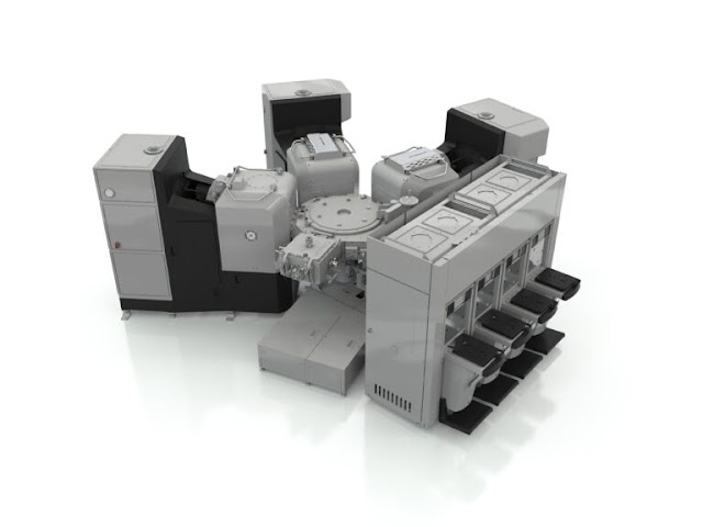
San Francisco, USA – ASM International N.V. (Euronext Amsterdam: ASM) today introduced the SONORA® vertical furnace system with dual reactor chambers for 300mm wafers. The system’s dual boat reactors produce the highest available throughput in its class, increasing reactor utilization to virtually 100%, while ensuring the lowest capex.


SONORA is named after the blossoming Sonoran desert near Phoenix, Arizona. The look and feel of the SONORA system reflects the colors of the Saturn rockets from the Space Age - a time when semiconductor technology was given a huge boost. It is also the era that gave birth to ASM, and so the SONORA® color scheme creates a link to ASM’s more than 50-year legacy in semiconductor processing equipment. LINK: SONORA_vertical_furnace (asm.com)

“The introduction of the novel SONORA® system is part of our strategy to selectively grow our vertical furnace presence in the market. The new SONORA® ensures that ASM will be strengthening its offering in advanced logic/foundry and memory applications as well as extend our leadership position in the market for More than Moore (such as analog and power) applications,” said Hichem M’Saad, Chief Technology Officer and Member of the Management Board.

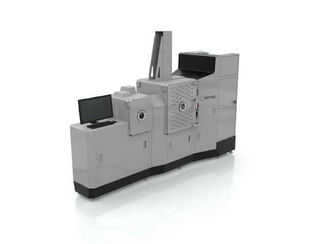
The new SONORA® is fully compatible with the original A412™, so existing process recipes are easily transferred, accelerating system qualification and ramp up. System deliveries have begun to multiple customers globally, among them leaders in advanced logic, and power device manufacturing.

ASM’s predecessor A412™ vertical furnace system has a proven track record of more than 1,000 reactors shipped to customers worldwide and over 22 years of maturity in semiconductor manufacturing. The new SONORA® has a novel system architecture that maximizes floor space productivity as well as service area. Its dedicated process modules have individually controlled high purity mini environments. Our innovative gas injection system for low pressure processing provides the best uniformities of deposited films between the individual wafers at larger load sizes. These larger process wafer load sizes combined with the updated control system, new robots, faster wafer cooldown, faster boat exchange modules generate up to 30% more productivity, compared to its predecessor. Higher productivity also results in lower energy and chemical usage per wafer. Special attention was given to the design for serviceability leading to a spacious access for all maintenance activities. The new system has been further modernized with an intuitive graphical user interface, predictive maintenance by advanced control diagnostics, and plug & play installation. Customers can count on the SONORA® delivering increased reliability and better ease of use with production output that achieves better repeatability, productivity, and time utilization.


The A412 PLUS is for 300mm wafers, while the A400 is for 200mm and smaller wafers sizes

Like its predecessor, the SONORA® offers a comprehensive portfolio of process applications including low pressure chemical vapor deposition (LPCVD) processes like doped silicon and silicon nitride films, diffusion processes such as wet oxidation and anneal processes, as well as a leading portfolio of atomic layer deposition (ALD) materials.

Thursday, June 23, 2022

How Forge Nano is Engineering the Future, One Atom at a Time

Utilizing proprietary nano-coating technology, Forge Nano is able to fundamentally improve nearly any material on earth at the atomic level.

THORNTON, Colo., June 23, 2022 (Newswire.com) – Forge Nano, leaders in atomic layer deposition (ALD) technology and equipment, are working to unlock the next generation of materials science. Through a full product line of ALD equipment addressing large scale manufacturing all the way down to fundamental R&D, Forge Nano has developed nano-coating solutions that are cost-effective, and can improve nearly any product from the atoms up.

“For decades, ALD has been relegated to bench-top exercises and the world of peer-reviewed articles,” says James Trevey, Ph.D., CTO of Forge Nano. “It’s like we’re selling wireless internet in a world of Cat 5 ethernet cables. ALD delivers greater performance for a lower cost than incumbent technology for nearly any application, and now we have brought this technology to the commercial environment at true manufacturing scale.”


Atomic Layer Deposition (ALD) is a surface engineering technique whereby an extremely thin coating (as thin as a single layer of atoms) is applied to a wide range of materials, powders, or objects. This process can be repeated to build up multiple layers on nearly any surface, producing robust coatings that can be engineered to enhance or add to the characteristics of the material being coated.

Conventional coating techniques such as physical vapor deposition (PVD) and chemical vapor deposition (CVD) have been the standard techniques used in many industries in the past, but as ALD is now available for any material at commercial scale, their time is limited. Forge Nano’s team of scientists and engineers have developed a line of ALD tools that make the technology cost-effective and practical to apply in small-scale lab environments all the way up to full-scale commercial manufacturing settings. Case in point – Forge Nano has already demonstrated commercial success in many markets, including batteries, pharmaceuticals, and semiconductors.

Batteries – Making better, longer lasting, safer batteries

Forge Nano ALD coatings have been demonstrated to improve energy density, lifetime, safety, and cost of batteries. In an electric vehicle these benefits would translate to a lower cost, longer range, faster-than-fuel recharge times, and an EV battery that can last for at least 20 years and is better suited for recycling than current EV batteries. Forge Nano’s ALD techniques have also been shown to be more cost effective, more efficient, more precise, and more environmentally friendly than batteries made with other coating techniques.

Pharmaceuticals – Imagine controlled, single-dose, temperature-stable vaccines that can be effectively distributed around the globe without the fear of spoilage.

Forge Nano ALD coatings have been used by pharmaceutical companies to apply various characteristics to medications or vaccines. ALD coatings can make a vaccine thermostable, eliminating the need for refrigeration. Time release properties can be applied as well, allowing multiple doses to be combined into a single treatment or injection. This can make the medication or vaccine easier to distribute to rural areas and eliminates the need for additional doses or boosters.

Semiconductors – Optimizing Next-Gen devices at the atomic scale.

Forge Nano ALD coatings can be applied to semiconductor wafers and components to create hermetic, pin-hole free, low stress thin films that offer excellent uniformity and precision required by semiconductor manufacturers. In addition to producing superior coatings, Forge Nano tools can produce ALD coatings faster and more efficiently than anyone else, making Forge-enabled semiconductors

Thanks to the scalability of Forge Nano’s extensive research and development, ALD technology that was once thought of as too expensive is now accessible and practical even at the smallest of scales. Forge Nano is using its manufacturing expertise to provide R&D equipment to universities, national labs, and centers of excellence, establishing ALD as a viable commercial pathway for materials science researchers. This is contrasted by the many companies Forge Nano has worked with to integrate ALD into their manufacturing processes, installing high-volume equipment capable of coating enormous amounts of materials, powders or objects.

For those not ready to make the investment in Forge Nano’s ALD equipment, R&D and toll coating services are available as well. Forge Nano offers their world-class ALD technical team to develop coating solutions and run proof of concept tests. Forge Nano is also uniquely equipped to offer toll coating services, where an organization may entrust Forge Nano to produce the ALD coatings with their in-house equipment.

To find out more about Forge Nano’s proprietary atomic layer deposition (ALD) processes and equipment, visit ForgeNano.com.

Wednesday, June 22, 2022

NCD supplied ALE and ASD equipment to Samsung Electronics Co., Ltd.

NCD has recently supplied ASD (Area Selective Deposition) equipment to Samsung Electronics Co., Ltd. Following ALE (Atomic Layer Etching).

This is the cluster system which consists of two process modules (PMs) and a wafer transfer module (TM) and applies a running program for process integration. In addition, it is equipped to process at high temperatures up to 500℃ and process with ozone and plasma for developing the next semiconductor devices.

ALE is able to etch a deposited layer by atomic scale as opposed to ALD and ASD can only deposit on the selective area not grow the whole area of substrates by ALD.

Today, lots of universities, institutes, and companies have actively been developing future high-tech and highly integrated devices using ALE and ASD processes.

NCD expects that the ALE/ASD system will contribute very much to the development of high-end semiconductor technology and is going to do all of the efforts to the best ALD equipment company with new challenges and continuous R&D.

<Lucida M200PL Series ALD System>


Friday, June 10, 2022

Atomic Layer Deposition Expected to Grow to Meet Demand for More-than-Moore Devices and Applications

(Interview by SEMI) Atomic Layer Deposition (ALD) players are poised to seize a new growth opportunity after the chip shortage pushed manufacturers to announce fab capacity expansions worldwide. Geared toward 200mm market needs, 300mm ALD platforms have recently advanced to meet the demand of More-than-Moore (MtM) devices and applications for MEMS, sensors, power and RF devices, photonics. Driven by the wafer production volume increase, ALD solutions are now expected to grow and enter the MtM devices market.


SEMI spoke with Dr. Patrick Rabinzohn, Strategic Development Executive of Semiconductor ALD at Beneq, about the benefits of ALD and shared how Beneq is building a comprehensive ALD product portfolio – from Beneq Transform® to ProdigyTM – covering different device applications and wafer sizes. We also talked about Beneq solutions to customer challenges, thanks to its vision and future trends for MtM devices for ALD.

SEMI: Beneq is already a familiar name in the ALD equipment business. For those new to the brand, please introduce the company.

Rabinzohn: Beneq is the home of atomic layer deposition and has ALD in its DNA. In fact, the very first industrial application of ALD was done in 1984 here on electroluminescent displays – the same location where Beneq still is headquartered today! Beneq was formed in 1984 and today we are a leading provider of ALD solutions for More-than-Moore semiconductor device fabrication with the Beneq Transform®.

Beneq’s state of art applications lab enables proof-of-concept and customer adoption for new ALD processes. Our team of engineers and experts is dedicated to making ALD tools accessible to our customers and partners.

SEMI: Beneq introduced the first Beneq Transform® in late 2019. How has adoption been so far?

Rabinzohn: The Beneq Transform® has revolutionized ALD cluster tools for More-than-Moore semiconductor markets in the EU, the U.S. and Asia since its launch in 2019. As of November 2021, Beneq has seen higher than expected demand for both the Transform and Transform Lite product configurations across key customer regions such as Europe, Japan, China, Taiwan and the U.S. We are super excited to see more customers adopting ALD in their More-than-Moore applications.

Thursday, May 12, 2022

Picosun solution enables stretchable organic electronics manufacturing on large scale

ESPOO, Finland, 12th of May 2022 – Organic electronics enable everyday devices such as displays, lighting and sensors to have high energy efficiency, light weight and low manufacturing costs. These benefits have made organic electronics a mainstream technology today and great steps have been taken to realize the technology’s true potential. Finally, flexible and stretchable circuitry can be fabricated, paving the way for wearable devices and e-textiles.


This technological leap has left behind traditional encapsulation methods, such as heavy glass lids with limited stretchability. The biggest downside of organic electronics, however, is their susceptibility to oxidation by moisture. This moisture ingress can have a direct impact on device performance and longevity. To address this challenge, thin film encapsulation solutions (TFEs) have been introduced as a key technology, heavily relying on vacuum-based thin film deposition techniques like atomic layer deposition (ALD). Ultra-thin ceramic ALD films serve as an effective moisture barrier but can crack under stress unless combined with more elastic molecular layer deposition (MLD) films.

Picosun has brought a stable MLD process to the realm of batch processing with PICOSUN® P-300B ALD tool with batch sizes up to 27 pieces of 200 mm wafers. The results show wafer-to-wafer uniformity of 1% and several Å/min growth rates. When combined with ALD in a nanolaminate, the resulting TFE can resist defects when up to 2% tensile stress is applied and the coatings exhibit a steady-state and effective water vapour transfer rate (WVTR) in a range of 10-6 g/m2*d in ambient conditions, when measured from a very large sample area (3320 mm2) to reflect a real-world application.

“We see immense possibilities for our customers with the Picosun’s proven capabilities of depositing ultra-barrier performance TFEs on large scale. As an example, the future OLED manufacturing can be upscaled without fearing for the reliability of the devices”, states Juhana Kostamo, VP, Industrial Business Area of Picosun Group.

Monday, May 2, 2022

NCD supplied additional ALD equipment for special protective coating

Recently NCD supplied additional ALD equipment to the customer based in Korea. It is for coating products used in semiconductor equipment to protect from corrosion and plasma arcing.

This re-contracted equipment is Lucida GSH Series ALD. It is a fast and efficient ALD protective layer coating system with lower precursor usage than existing equipment. The customer is looking forward to extending the lifetime of high cost products through uniform and high quality ALD coating.

This repeat ordered supply shows that the customer has had confidence in the NCD’s ALD technology and the excellence of the equipment.


<LucidaTM GSH Series ALD>

Wednesday, April 6, 2022

Senior Process Engineer I- Coating at ASM Phoenix AZ

About the job

We’re not like most. We don’t just overcome obstacles – we don’t see them. Instead, we see the potential in every person, and every situation. We don’t wait for opportunity to appear – we create it. Meet ASM. A company that has been searching for people just like you.


Job link: (21) Snr Process Engineer I- Coating | ASM | LinkedIn

Who is ASM?

ASM is a leading, global supplier of semiconductor wafer processing equipment. Our ambitious team is dedicated to delivering innovative technology solutions to the world’s leading semiconductor manufacturers. We have over 2,600 employees based in 14 countries, including Belgium, Japan, Netherlands, South Korea, Singapore, Taiwan and United States. Together we work to develop Epitaxy, ALD, PEALD, Vertical Furnaces and PECVD thin-film deposition technologies for our customers. Our goal is to remain an industry leader by being ahead of what’s next. We accomplish this by focusing on finding collaborative solutions to make integrated circuits, or chips, smaller, faster and even more powerful.

ASM, an inclusive workplace

We at ASM are a truly global organization that works diligently with an open-mind in all areas of our business. We strive for a culture and work style that fosters trust and transparency. We put our people first, and that is how we will continue to succeed. We are an equal opportunity employer and value diversity. We recognize and value the differences between individuals, including gender, ethnicity, religious beliefs, sexual orientation, knowledge and experience, work background, age, skills, amongst others. Recruiting and developing a diverse workforce provides a wide range of perspectives. This enables a culture of continuously exploring and adopting new technological ideas and innovations, and it also enables us to deliver excellent products and service to our clients.

Essential Functions
  • Work with a safety-first mentality
  • Drive ASM process protocol with emphasis and regularly institute or update service solutions to the field
  • Work on assigned CIP projects, develop DOE’s and communicate openly both internally and externally.
  • Focus on refresh of IP for legacy products and influence new design IP.
  • Provide “novelty” to items making them hard to reproduce
  • Improve upon existing design for performance and cost efficiency
  • Generate project scope documentation and prepares specific project reports against identified schedule.
  • Building stakeholder consensus to deliver approach
  • Collaboratively manages global stakeholders including end users, technicians, engineers, procurement, spares, manufacturing, subject matter experts as well as management in both business and / or operations to project specific details.
  • Applies project management principles to produce cooperative and collaborative efforts, deliver business strategic objectives and fill the end customer needs.
  • Consistently provide quality solutions to field and customer personnel and create new BKM’s.
  • Exercise good judgment within broadly defined practices and policies in selecting methods, techniques, tools and evaluation criteria for obtaining desired results
  • Be willing to travel domestically and internationally as required.

Education /Experience
  • BS or MS Degree in Mechanical engineering, Electrical Engineering, Material Science or related degree required.
  • 5+ years of experience in the semiconductor field.
  • Equipment Engineering experience with design, and development of complex mechanical systems including comprehension of: reactors, vacuum systems and chambers, gas delivery systems, abatement systems, pneumatics, water cooling, and circuits required. Ability to implement, maintain, improve electrical instruments, equipment, facilities, components, products, systems and provide novel solutions for the semiconductor equipment industry. Comprehension of PLC's and functionality.
  • Should have a broad based background in analysis and debug of complex electrical and/or mechanical systems
  • Semiconductor capital equipment experience is preferred.
  • Understanding of materials: metals, plastics, surface coatings and surface finishes.
  • Deposition product knowledge a plus (CVD, ALD, EPI, PVD). Knowledge of ASM Emerald tool distinct plus.
  • Design applications Pro/ENGINEER, AutoCAD, and Hands on experience with FEA and CFD analysis preferred. Solid ability to read and understand P&IDs, Electrical, and Mechanical schematics and drawings.
  • Proficiency in ANSI Y14.5 geometric dimension and tolerance.

Skills
  • Ability to rectify a challenging situation and gain customer (Internal and external) confidence
  • Strong positive attitude, ability to work in a team environment and work alone. Able to drive meetings, both internal and external, with excellent internal ASM relations
  • Ability to work responsibly with all ASM resources and departments in a multifunctional high paced atmosphere with minimum supervision on highly complex problems
  • Ability to handle multiple tasks simultaneously and be able to organize and run projects
  • Strong computer skills, working knowledge of MS Word, Excel, PowerPoint, SharePoint, Project, and SAP
  • Drive ASM SOP’s and protocol, able to guide co-workers toward common goals
  • Become an active member of ASM GSS core teams
  • Excellent communication skills; speak and write in a clear and concise manner, and ability to accurately and fully convey issues to peers, management, or customers
  • Strong organizational skills and leadership qualities
  • Accurate, timely reporting
  • Parts tracking, ordering, managing, Setting BOM levels
  • Technical writing background. Ability to create procedures, written in an informative manner that eliminates ambiguity and personal interpretation
  • Training skills, be able to communicate with customers and their employees on maintenance procedures, preventative maintenance, and operating specific equipment. Be the content expert with ability to provide onsite support when needed
  • Process comprehension, be able to understand basics of creating process recipes focusing on the ALD process.
  • Understanding of chemistry interactions with different materials. Gas and liquid chemistry knowledge is a bonus
  • Experience with Equipment installs Organizing/Coordinating trades, SL1, SL2, commissioning and qualifications to specific standards.
  • SPC creation with JMP/Statistical analysis and ability to drive root cause solutions through data driven decisions

From the very start of the semiconductor industry to the present day, we’ve been technology leaders who have pioneered innovation and brought new processes into mainstream manufacturing. We are collaborating, creating, and delivering on our vision – a shared vision to drive innovation with new technologies and delivering excellence with dependable products. By doing this, we’ll create new possibilities for everyone to understand, create and share more of what they love.

Be part of our exciting future and join our team today!

Thursday, March 10, 2022

Beneq fulfills customer demand for tailored ALD equipment services and support with BeneqCareTM

Beneq, the home of Atomic Layer Deposition (ALD), has introduced BeneqCare, a new modular solution to offer support and maintenance services to organizations that own and operate Beneq ALD equipment.

Beneq leads the market with ALD products for R&D, semiconductor device fabrication, 3D and batch production, ultra-fast spatial ALD (C2R), and roll-to-roll ALD. Today, the company has launched BeneqCare to help customers in the EU, Asia and the USA maximize the value of their ALD tools throughout their equipment’s life cycles.


“We have been investing heavily in widening our service capabilities worldwide. Now, we offer service coverage in all regions. We have also established spare part hubs in every region at Beneq offices,” says Hans Fabritius, Vice President, Life Cycle Services at Beneq.

“BeneqCare simplifies ALD equipment ownership by helping our customers maximize uptime and gain access to the right support at every stage of their tool’s life cycle. We are ready to assist our customers in meeting their productivity requirements –from training personnel in using the equipment to meeting any unscheduled maintenance or spare parts needs,” asserts Fabritius.

BeneqCare provides Beneq customers who operate in the industrial and research sectors with a wide range of service modules to suit their operations, from extended warranty and training services to remote or onsite support.

“Our customers have high expectations for the performance of their Beneq ALD tools. BeneqCare brings them versatile support and service plans that grow with their businesses,” says Fabritius.

Companies and research facilities that have commissioned Beneq ALD equipment can avail of a variety of BeneqCare service modules to suit their unique requirements. Among the BeneqCare modules are technical support services, including remote support via Augmented Reality (AR); spare part services; extended warranties; preventive as well as unscheduled maintenance services; and training.

Learn more about BeneqCare.


Wednesday, March 2, 2022

Japanese Samco Opens Research Center for Nano Thin Films & Materials to accelerate ALD Development

Japanaese Samco plans to increase its number of researchers at the Research Center from the current 8 to 20 in the next 3 years and to expand its annual ALD systems sales to 3 billion yen in five years.

Wednesday, December 8, 2021

Meaglow Hollow Cathode Gas Plasma Source Paper Published by the Journal “Coatings”

Meaglow technical staff have published a paper entitled: “Recent Advances in Hollow Cathode Technology for Plasma-Enhanced ALD — Plasma Surface Modifications for Aluminum and Stainless-Steel Cathodes” in the journal “Coatings”. An early version of the paper can be accessed at the journal website, here.

The paper provides a brief review of oxygen contamination from ICP and microwave legacy sources, but also provides details of the operation of the hollow cathode gas plasma sources now widely used by the ALD community.


Tuesday, December 7, 2021

Beneq unveils two new ALD products for 300mm and compound semiconductor device fabrication respectively

Beneq revolutionized ALD cluster tools for More-than-Moore device makers with the highly successful Beneq Transform® family of products. Today, Beneq broadens its product portfolio further with two new distinct solutions: the Transform® 300 and ProdigyTM.

The Beneq Transform 300 and Prodigy were each created in response to specific technology requirements in the semiconductor manufacturing sector.

“The Transform 300 is designed to meet the growing demand of emerging semiconductor applications at 300 mm for devices such as CMOS image sensors, Power Devices, Micro-OLED/LED, and Advanced Packaging, which call for a high degree of versatility,” explains Patrick Rabinzohn, Vice President, Semiconductor ALD at Beneq.

“We created Prodigy to address those market segments that need a simple solution supported by high-end technology. It inherits the ALD design and processing knowhow we at Beneq have developed over the last 15 years, packing advanced features in a simpler, targeted industrial form factor,” continues Rabinzohn.
Beneq Transform 300 is the only 300 mm ALD cluster tool that combines thermal ALD (batch) and plasma ALD (single wafer) technologies to provide a highly versatile platform for IDMs and foundries. It is dedicated to advanced thin-film applications in CIS, Power, Micro-OLED/LED, Advanced Packaging and other MtM applications.

Beneq Tranform 300 is a highly configurable platform that caters to multiple advanced thin-film applications ranging from gate dielectric including in high aspect ratio trenches, to anti-reflection coating, final passivation or encapsulation, Chip-Scale-Packaging and beyond.

Beneq Prodigy is the deal manufacturing solution for compound semiconductor including RF IC’s (GaAs/GaN/InP), LED, VCSEL, Light Detectors and for MEMS manufacturers and foundries looking to enhance device performance and reliability through an affordable stand-alone ALD batch tool. Beneq Prodigy provides best-of-breed passivation and encapsulation films across multiple wafer types and sizes.

To learn more, visit:


Tuesday, November 9, 2021

Innovative remote plasma source for atomic layer deposition for GaN devices

Oxford Instruments and TU Eindhoven present results from the new Atomfab(TM) Remote Plasma ALD system for high-quality dielectric films. This could enable GaN normally off high-electron-mobility transistors (HEMTs).

Innovative remote plasma source for atomic layer deposition for GaN devices
Journal of Vacuum Science & Technology A 39, 062403 (2021); https://doi.org/10.1116/6.0001318

High-quality dielectric films could enable GaN normally off high-electron-mobility transistors (HEMTs). Plasma atomic layer deposition (ALD) is known to allow for controlled high-quality thin-film deposition, and in order to not exceed energy and flux levels leading to device damage, the plasma used should preferably be remote for many applications. This article outlines ion energy flux distribution functions and flux levels for a new remote plasma ALD system, Oxford Instruments Atomfab™, which includes an innovative, RF-driven, remote plasma source. The source design is optimized for ALD for GaN HEMTs for substrates up to 200 mm in diameter and allows for Al2O3 ALD cycles of less than 1 s. Modest ion energies of <50 eV and very low ion flux levels of <1013 cm−2 s−1 were found at low-damage conditions. The ion flux can be increased to the high 1014 cm−2 s−1 range if desired for other applications. Using low-damage conditions, fast ALD saturation behavior and good uniformity were demonstrated for Al2O3. For films of 20 nm thickness, a breakdown voltage value of 8.9 MV/cm was obtained and the Al2O3 films were demonstrated to be suitable for GaN HEMT devices where the combination with plasma pretreatment and postdeposition anneals resulted in the best device parameters.


Image of the Oxford Instruments Atomfab system (a) used in this work. A conceptual schematic (b) of the plasma source with powered (light gray) and grounded (dark gray) surfaces indicated. This plasma source was also put on a testbed system (c), which was used for the ion measurements and OES, the RFEA for probing the ion energy, and the flux was placed at the wafer level. Besides the RFEA, the testbed system was designed to allow for a range of optical diagnostics in the future (d).


Growth per cycle for ALD of Al2O3. Data are given as a function of precursor (a) and plasma (b) dose times and the respective purge times (c) and (d) at 300 °C. Single and double exponential curve fits serve as a guide to the eye.


Tuesday, October 26, 2021

Benchtop ALD system AT410 from Anric Technologies offered by SPS

SPS offers various ALD systems, including a table top version for surface controlled layer-by-layer deposition with atomic layer accuracy. We are talking about the AT410! This system provides a solution to conformal, conductive thin films for 3D sample prep, as well as traditional 2D coatings that are currently grown using sputtering/evaporation. It not only pushes boundaries, but it’s also an effective replacement for your current sample preparation processes, all within a benchtop configuration!


Thursday, October 14, 2021

Picosun ALD move into HVM for Optoelectronics at ams OSRAM

ESPOO, Finland, 28th of July 2021 – Picosun Group delivers cutting-edge Atomic Layer Deposition (ALD) technology to ams OSRAM for volume manufacturing of optical semiconductor devices.

ams OSRAM has invested in a fully automated PICOSUN® Morpher production cluster, which can deposit multiple materials on a batch of wafers even during the same process run. The flexibility and process variety of the PICOSUN® Morpher system is a key advantage, which enables volume production as well as the testing of new processes for R&D of future products.


Picosun Group and ams OSRAM have collaborated in a public funded project FLINGO (m-era.net project) to develop new ALD materials and processes to improve the characteristics of LEDs, such as efficiency and durability. The collaboration between the parties will continue after the ALD system delivery with activities to further expand the use of ALD in optoelectronic semiconductor processing.

“We have been working with Picosun since 2010 and now with this investment we can bring our collaboration to the next level. We are very excited to have the PICOSUN™ Morpher F cluster platform installed in our cleanroom”, states Dr. Sebastian Taeger, at ams OSRAM.

“The optical semiconductor market is one focus area of Picosun today. It is a fast-growing market where we have a strong presence with our tailored solutions for compound semiconductor-based devices. We have had excellent collaboration with the ams OSRAM technical team during project FLINGO and during the system specification stage. The expertise from both companies has resulted in optimized ALD solutions to boost the performance of the customer’s products.”, continues Dr. Christoph Hossbach, General Manager of Picosun Europe GmbH.

Saturday, October 2, 2021

ASM International Investor Day take away - the leader in ALD wafer processing equipment for the booming semiconductor industry

 ASM International, the leader in ALD wafer processing equipment for the booming semiconductor industry recently hold its annual investor day.

Highlights included:
  • Targeting revenue of €2.8-€3.4 billion by 2025 (2020-2025 CAGR of 16%-21%), gross margins of 46%-50% in 2021-2025, and operating margins of 26%-31% in 2021-2025;
  • Targeting Net Zero emissions by 2035 and 100% renewable electricity by 2024;1
  • Single-wafer ALD market expected to increase from $1.5 billion in 2020 to $3.1-3.7 billion by 2025;
  • Further capacity expansion of our new manufacturing facility to be production ready by early 2023.

3D device architecture evolution is continuing into all leading-edge semiconductor components. 3DNAND and FinFET are to be followed by GAA FETs and 3D-DRAM. Together with the need for new materials drives the demand for CVD and ALD processing equipment (ASM Investor Day 2021)

“I’m very excited to share the strong prospects for our company during our first Investor Day,” said Benjamin Loh, CEO of ASM International. “We project revenue to increase to €2.8–€3.4 billion by 2025, with operating margins of 26%-31% during the 2021-2025 period. Key inflections in next generation semiconductor devices such as complex 3D architectures and new materials, are expected to drive double digit growth in ASM’s key markets. Today we will also highlight new innovations in our products, enabling our customers’ technology roadmaps. Capitalizing on our innovative strength, early customer engagements and product differentiation, we are focused on maintaining our leading position in the ALD market and to further increase our market share in Epi.


The semiconductor market, historical and as forecasted by VLSI Research. By 2030 it will have doubled to USD 1 Trillion. (VLSI Research - ASM Investor Day 2021)

In view of the strong growth opportunities ahead of us we will further step up our R&D investments and strengthen our capabilities. In addition, with our new expanded manufacturing facility in Singapore completed just less than one year ago, we have now decided to prepare a further substantial capacity increase within this facility to be production ready by early 2023.


The Wafer Equipment market growth has reached a new level and will sustain it for years to come (VLSI Research - ASM Investor Day 2021).


ASM controls more than 50% of the single wafer ALD equipment market and intends to defend the market share going forward to 2025. The market is forecasted by ASM to more than double 2020 to 2025, reaching USD 3.1 to 3.7 billion by then. (ASM Investor Day 2021)

A further increase in our ambition to sustainability is a central element in our strategy. As an important next step we announce today our ambitious target to achieve Net Zero emissions by 2035 (scope 1, 2 and 3) and 100% renewable electricity by 2024. As we continue to drive growth through innovation, ASM is well positioned to create long-term value for all its stakeholders.”


ASM Roadmap for DRAM, 3D-NAND and Logic,  aligned with its leading-edge customer base. (ASM Investor Day 2021)

The Investor Day was held at 2:00 pm CET  and Q&A can also be followed through a live webcast after registering at: https://investorday.asm.com.

Presentation:LINK

UPDATE Q3 2021 GUIDANCE

ASM also announced that Q3 order intake is expected to be above €600 million, compared to previous guidance of €510-530 million, mainly driven by continued strong demand in the logic/foundry sector. Q3 net sales are expected to be in line with previous guidance €400-430 million.

Friday, September 3, 2021

The world’s largest ALD system - The BENEQ P1500 is here!

Now it is here - The Beneq P1500 is the biggest ALD system and is built specifically to coat sizeable sheets and complex parts. It is also made to deliver increased throughput for batches of smaller components.


Beneqs customers use the P1500 for optical coatings on large diameter substrates, anticorrosive coatings of semiconductor equipment parts, and various applications where ALD is used on glass or metal sheets.


Large parts need large ALD tools. The Beneq P1500 can accommodate parts up to 1300 × 2400 mm in size, and enables the deposition of high-quality, functional optical coatings on wide area mirrors or lenses. It is also used to coat batches of parts in the 300 to 1000 mm size range.

More information: LINK


Wednesday, September 1, 2021

Picosun strengthens its position in the semiconductor market

ESPOO, Finland, 31st of August 2021 – Picosun Group strengthens its position in the 300 mm semiconductor market with its new generation ALD tool PICOSUN® Sprinter.


PICOSUN® Sprinter was first launched in December 2020 as a stand-alone module. Now also customer deliveries and installations of PICOSUN® Sprinter clusters have started.

“A Sprinter cluster consist of two Sprinter modules and a central vacuum wafer-handling robot utilizing 5-wafer handling. The set-up enables a throughput of more than 100 wafers an hour with 10 nm aluminium oxide target film thickness”, explains Juhana Kostamo, VP, Industrial Business Area of Picosun Group.

“The throughput capability combined with the unique design of the tool’s reaction chamber, the record-breaking batch film quality and the fact that the tool can be fully integrated with the customers’ production line, makes PICOSUN® Sprinter the tool of choice for semiconductor, display and IoT component industries who need a future-proof tool with single wafer film quality and uniformity in fast batch processing”, Kostamo concludes.

Thursday, July 29, 2021

Picosun delivers ALD Morpher 200 mm Batch Cluster tool to ams OSRAM

ESPOO, Finland, 28th of July 2021 – Picosun Group delivers cutting-edge Atomic Layer Deposition (ALD) technology to ams OSRAM for volume manufacturing of optical semiconductor devices.

ams OSRAM has invested in a fully automated PICOSUN® Morpher production cluster, which can deposit multiple materials on a batch of wafers even during the same process run. The flexibility and process variety of the PICOSUN® Morpher system is a key advantage, which enables volume production as well as the testing of new processes for R&D of future products.


Picosun Group and ams OSRAM have collaborated in a public funded project FLINGO (m-era.net project) to develop new ALD materials and processes to improve the characteristics of LEDs, such as efficiency and durability. The collaboration between the parties will continue after the ALD system delivery with activities to further expand the use of ALD in optoelectronic semiconductor processing.

“We have been working with Picosun since 2010 and now with this investment we can bring our collaboration to the next level. We are very excited to have the PICOSUN™ Morpher F cluster platform installed in our cleanroom”, states Dr. Sebastian Taeger, at ams OSRAM.

“The optical semiconductor market is one focus area of Picosun today. It is a fast-growing market where we have a strong presence with our tailored solutions for compound semiconductor-based devices. We have had excellent collaboration with the ams OSRAM technical team during project FLINGO and during the system specification stage. The expertise from both companies has resulted in optimized ALD solutions to boost the performance of the customer’s products.”, continues Dr. Christoph Hossbach, General Manager of Picosun Europe GmbH.

Friday, July 2, 2021

Future foldable and flexible Display with NCD’s ALD encapsulation technology

In the global market of smart phones, competition on mobile’s form factors has been an important issue since foldable smart phones had launched following cured ones. Samsung electronics applied in-folding form factor to Galaxy Fold and Galaxy Z Flip, and Huawei used out-folding form factor to Mate X. New two or three folding form factor has been unveiling to the public beyond in-folding and out folding displays.

Flexible displays consist of Thin Film Transistor (TFT), Organic Light Emission Diode (OLED) and multi encapsulation layers. Generally organic and inorganic laminated layers is used for foldable displays and PECVD has applied to deposit inorganic materials.

Basically, Inorganic layers is lack of brittleness then their encapsulation property is degraded with continuous mechanical stress. ALD method for TFE was considered instead of PECVD due to their excellent encapsulation characteristics with thicknesses of few tens of nanometers. The reliability of the tool blocked applying to production at that time.

But because of the superior encapsulation property using ALD, many universities, institutes as well as display companies have been developing ALD inorganic layers for flexible displays and evaluating hundreds of thousand times folding test considering actual use recently.

LucidaTM GD Series ALD


The customer which has NCD’s Lucida GD Series ALD, measured folding test on flexible displays with inorganic layers using ALD instead of using PECVD and showed great performance under actual display operation. The 5.85 inch AMOLED display panels for in-folding and out-folding consisted of encapsulation structure of 30nm Al2O3 ALD/ 8㎛-Polymer/ 30nm Al2O3 and was tested in-folding and out-folding evaluation of 200,000 times with bending radius of 2R under light status after the 1st reliability test of RA 60℃/90% for 500hr. There were no dark spots on the panels after finishing the folding measurement. The 2nd reliability test of RA 60℃/90% for 48hr followed folding evaluation and then the TFE status was examined without any cracks.


Using NCD’s large area batch ALD system for foldable phones could obtain superior encapsulation property and flexibility with very thin inorganic layers to current ones using PECVD as well as provide great productivity because the batch tool can process lots of panels at one time.

Then NCD really looks forward to applying its large area batch ALD technology to encapsulation of future flexible display with in/out-folding and very small bending radius because of having solved the previous issues without both reliability and productivity that the reason is why ALD equipment didn’t apply for mass production of flexible display.

Thursday, June 24, 2021

Picosun strengthens its presence in Southeast Asia

ESPOO, Finland, 24th June 2021 – Picosun Group extends its global sales and service partner network further by signing a partner agreement with Hermes-Epitek Corporation Pte. Ltd. Hermes-Epitek Corporation, headquartered in Taiwan, is one of the world’s largest high-tech equipment distributors. The company provides equipment for semiconductor and optoelectronic manufacturing, as well as tech services and parts sales.


“We look forward to cooperate as Picosun’s sales representative and external field service provider targeting both 8-inch and 12-inch ALD markets in all Southeast Asia countries”, states Teo Kim Leong, Director, Hermes-Epitek Corporation.

“Southeast Asia is one of Picosun’s important market areas, where the demand for industrial ALD solutions is constantly increasing. For almost ten years now, Picosun has successfully provided world leading ALD solutions to numerous customers and partners in both academies and industries in Southeast Asia. I’m happy that with the partnership with Hermes-Epitek Corporation we are able to serve our customers in the region even better”, says Edwin Wu, CEO, Picosun Asia Pte. Ltd.

Picosun provides the most advanced AGILE ALD® (Atomic Layer Deposition) thin film coating solutions for global industries. Picosun’s ALD solutions enable technological leap into the future, with turn-key production processes and unmatched, pioneering expertise in the field – dating back to the invention of the technology itself. Today, PICOSUN® ALD equipment are in daily manufacturing use in numerous leading industries around the world. Picosun is based in Finland, with subsidiaries in Germany, USA, Singapore, Japan, South Korea, China mainland and Taiwan, offices in India and France, and a world-wide sales and support network. Visit www.picosun.com.

More information:
Edwin Wu
CEO
Picosun Asia Pte. Ltd.
Tel. +358 40 480 3449