Showing posts with label HKMG. Show all posts

Friday, March 26, 2021

Samsung confirms first HKMG for DDR5 DRAM

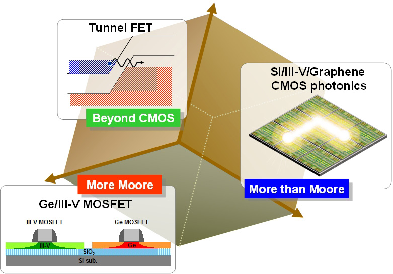
ASM International recently acknowledged that ALD High-k/Metal Gate (HKMG) is finally in high volume production for DRAM (LINK). Now Samsung confirms that. This is a small victory for all people working on this process for such a long time. My first tool ownership when I moved to Germany and started at Infineon was an ASM Polygon 200 mm cluster with a Pulsar 2000 chamber running HfO2, TiN, TiHfN, TiAlN, Al2O3, and my not fully understood HfN ALD process and a Poly chamber that I never really cared too much about. Press release below - and now do the maths - how big this business is once rolled out for all DRAM technologies to come - yeah $$$, many tulips indeed.


Samsung Develops Industry’s First HKMG-Based DDR5 Memory; Ideal for Bandwidth-Intensive Advanced Computing Applications

512GB capacity DDR5 module made possible by an 8-layer TSV structure
HKMG material reduces power by 13 percent while doubling the speed of DDR4


Samsung Electronics, the world leader in advanced memory technology, today announced that it has expanded its DDR5 DRAM memory portfolio with the industry’s first 512GB DDR5 module based on High-K Metal Gate (HKMG) process technology. Delivering more than twice the performance of DDR4 at up to 7,200 megabits per second (Mbps), the new DDR5 will be capable of orchestrating the most extreme compute-hungry, high-bandwidth workloads in supercomputing, artificial intelligence (AI) and machine learning (ML), as well as data analytics applications.


“Samsung is the only semiconductor company with logic and memory capabilities and the expertise to incorporate HKMG cutting-edge logic technology into memory product development,” said Young-Soo Sohn, Vice President of the DRAM Memory Planning/Enabling Group at Samsung Electronics. “By bringing this type of process innovation to DRAM manufacturing, we are able to offer our customers high-performance, yet energy-efficient memory solutions to power the computers needed for medical research, financial markets, autonomous driving, smart cities and beyond.”

“As the amount of data to be moved, stored and processed increases exponentially, the transition to DDR5 comes at a critical inflection point for cloud datacenters, networks and edge deployments,” said Carolyn Duran, Vice President and GM of Memory and IO Technology at Intel. “Intel’s engineering teams closely partner with memory leaders like Samsung to deliver fast, power-efficient DDR5 memory that is performance-optimized and compatible with our upcoming Intel Xeon Scalable processors, code-named Sapphire Rapids.”

Samsung’s DDR5 will utilize highly advanced HKMG technology that has been traditionally used in logic semiconductors. With continued scaling down of DRAM structures, the insulation layer has thinned, leading to a higher leakage current. By replacing the insulator with HKMG material, Samsung’s DDR5 will be able to reduce the leakage and reach new heights in performance. This new memory will also use approximately 13% less power, making it especially suitable for datacenters where energy efficiency is becoming increasingly critical.

The HKMG process was adopted in Samsung’s GDDR6 memory in 2018 for the first time in the industry. By expanding its use in DDR5, Samsung is further solidifying its leadership in next-generation DRAM technology.

Leveraging through-silicon via (TSV) technology, Samsung’s DDR5 stacks eight layers of 16Gb DRAM chips to offer the largest capacity of 512GB. TSV was first utilized in DRAM in 2014 when Samsung introduced server modules with capacities up to 256GB.

Samsung is currently sampling different variations of its DDR5 memory product family to customers for verification and, ultimately, certification with their leading-edge products to accelerate AI/ML, exascale computing, analytics, networking, and other data-intensive workloads


Wednesday, January 23, 2019

Strem Chemicals’ offers new La-FMD ALD precursor for future leading edge logic and memory products

Strem Chemicals’ offering of La-FMD is one of the most promising metal-amidinate ALD precursors for lanthanum (La) based ALD thin-films which are potentially strong candidates for high-k gate dielectric in the next generation of CMOS technology.

Rare earth elements have entered high volume manufacturing for advanced logic devices since the 32 nm node (IBM, Samsung and Globalfoundries – Chipworks 2010). Especially for Lanthanum (La) — the eponym of the lanthanide series in the periodic table has been implemented as a dopant in the high-k metal gate stack. Lanthanum oxide (La2O3, dielectric constant ~ 27), for example, has been explored for two decades as a high-k gate dielectric for the replacement of conventional silicon dioxide (SiO2) gate dielectric in the next generation transistors in logic as well as in dynamic random access memories (DRAMs).
Keyword segmentation of patent applications the last 20 years for Lanthanum and “Atomic Layer Deposition” [Patbase search 15 November 2018]

Atomic layer deposition is the most promising method for growing ultra-thin-films of La based gate dielectrics and has therefore been under extensive research and filing of patent applications in the last 20 years. The R&D effort has been focused on fields relating to dielectric and high-k dielectric applications in the semiconductor industry (see keyword segmentation above). The atomic layer-by-layer film growth facilitated by self-limiting surface reactions in ALD provides atomically precise film-thickness control, good uniformity across a large area substrate, and excellent conformality in case of high aspect ratio structures like modern FinFETs and memory capacitor type pillar structures. However, to work flawlessly it requires the ALD precursors that have specific properties (LINK): 

1. Sufficiently volatile (at least ~ 0.1 Torr equilibrium vapor pressure at a temperature at which they do not decompose thermally).

2. Rapidly vaporizing and at a reproducible rate (conditions that are usually met for liquid precursors, but not for solids).

3. Not self-reacting or decomposing on the surface or in the gas phase (for self-terminating surface reactions).

4. Highly reactive with the other reactant previously attached to the surface, which results in relatively fast kinetics and thus lower ALD temperatures and cycle times.

5. Volatile byproducts that can be easily purged in order to prepare for the subsequent half-cycle.

6. Non-corrosive byproducts to prevent non-uniformities due to film etching and corrosion of the tool.
In 2007, Intel Corporation incorporated HfO2 into high-k gate dielectric stack at 45 nm technology node. However, pure HfO2 suffers from low-k interface layer problem with Si, limiting lower equivalent oxide thickness (EOT) values. It also readily crystallizes at temperatures as low as ~500°C. Therefore, amorphous dielectrics with high thermal stability are still sought after for no intrinsic defects (e.g. grain boundaries), provided they still offer the advantages of HfO2, such as high dielectric constant, wide band-gap, and low leakage current. Lanthanum-based ternary oxides, such as lanthanum scandate (LaScO3) and lanthanum lutetium oxide (LaLuO3), deposited by ALD process involving metal amidinate precursors reportedly exhibit desirable structural and electrical properties. In fact LaLuO3 is potentially the best amorphous phase gate dielectric with dielectric constant k~32. It doesn’t form low-k interfacial layers with Si which enables effective oxide thickness (EOT) values < 1 nm with significantly low leakage current. Another factor contributing to the low leakage current across ALD grown thin LaLuO3 gate dielectric is the large band-offset (2.1 eV) with respect to Si; the symmetric conduction and valence band offsets result into equal leakage currents in electron driven NMOSFETs and hole driven PMOSFETs. It stays amorphous and doesn’t form alloys with Si or Ge after respective source/drain activation anneals.  


As a very recent example of an actual high aspect ratio application on 300 mm wafers requiring all ALD precursor characteristics described above (1 to 6) we can see the paper that Imec presented at this famous IEDM conference, on using a LaSiOx layer as a dipole inserted in the HKMG stack. Imec succeeded in stacking the complete FinFET front end module on top of a "standard" bulk silicon FinFET module demonstrating also good threshold voltage tuning, reliability and low-temperature performance. Presumably it has most likely been deposited by an ALD process since it will have to conformally coat the fins and ensure precise thickness control and uniformity : IEDM2018 Paper #7.1, “First Demonstration of 3D Stacked FinFETs at a 45nm Fin Pitch and 110nm Gate Pitch Technology on 300mm Wafers,” A. Vandooren et al, Imec [LINK].
As in this case and many more, the stringent qualifications for ALD precursors put them in the category of high quality specialty chemicals — the performance or function specific materials or molecules of choice. The deposited film properties are strongly influenced by the physical and chemical properties of a single molecule or a formulated mixture of molecules as well as its chemical composition. Therefore, it puts a lot of pressure on the manufacturer and supplier of the high purity specialty chemicals in terms of quality, purity, documentation procedures, customer service etc.

Thursday, June 16, 2016

Imec Demonstrates Gate-All-Around MOSFETs with Lateral Silicon Nanowires at Scaled Dimensions

LEUVEN, Belgium – June 16, 2016 – Today, at the 2016 Symposia on VLSI Technology & Circuits, nano-electronics research center imec presented gate-all-around (GAA) n- and p-MOSFET devices made of vertically stacked horizontal silicon (Si) nanowires (NWs) with a diameter of only 8-nm. The devices, which were fabricated on bulk Si substrates using an industry-relevant replacement metal gate (RMG) process, have excellent short-channel characteristics (SS = 65 mV/dec, DIBL = 42 mV/V for LG = 24 nm) at performance levels comparable to finFET reference devices.

TEM images of an NMOS GAASiNWFET(LG=70nm):(a)overview of the SiNW array; (b)detailed view of two stacked SiNWs.

 
GAA devices architectures offer optimal electrostatic control, thereby enabling ultimate CMOS device scaling. In addition, horizontal NWs are a natural extension of RMG finFETs, in contrast to vertical NWs which require more disruptive technology changes. Furthermore, stacking of NWs maximizes the drive current per footprint. Imec successfully combined these three aspects, and, for the first time, demonstrated vertically stacked horizontal Si NWs at scaled dimensions: 8-nm-diameter wires, 45-nm lateral pitch, and 20-nm vertical separation.

Compared to the conventional bulk FinFET flow, imec implemented two major differences in the process flow. First, shallow trench isolation (STI) densification at 750°C resulted to preserve sharp silicon-germanium (SiGe)/Si interfaces, which is essential for well-controlled Si NW release. Second, a low-complexity ground plane doping scheme was applied, suppressing the bottom parasitic channel.

“By demonstrating stacked nanowires with solid electrostatic control, at scaled dimensions, and using an industry-relevant RMG process on bulk silicon substrates, imec has achieved breakthrough results that can pave the way to realizing sub-10nm technology nodes,” stated Dan Mocuta, Director Logic Device and Integration at imec. “The upcoming research phase will focus on achieving even denser pitches and on leveraging this knowledge to develop gate-all-around lateral nanowire CMOS devices.”

Imec’s research into advanced logic scaling is performed in cooperation with imec’s key partners in its core CMOS programs including GlobalFoundries, Intel, Micron, SK Hynix, Samsung, TSMC, Huawei, Qualcomm and Sony.

Monday, February 8, 2016

Cubic High-k HfO2 by ALD on high mobility Germanium channels

High mobility Germanium is one of the most promising channel materials for future Logic, perhaps even at 7nm. Here is an open source paper (see abstract below) on using TEMAHf/H2O process for growing high symmetry cubic HfO2 on high mobility Germanium channel. It´s a joint work by University of Tokyo, Japan, and Zhejiang University, China. Until now all silicon based channel gate dielectrics are typically performed by using the HfCl4/H2O process. However, now moving too alternate high mobility channel materials like Germanium, InGaAsand other III/Vs it seem that the gate stack people will revisit the MO-precursors again - interesting!

 
The Takagi-Takenaka group researches the post-scaling semiconductor devices for low-power LSI and on-chip optical interconnection for: Ge/III-V MOSFETs, Tunnel FETs, Si photonics, III-V CMOS photonics, Graphene photonics and 2D material electronics (from Takagi and Takenaka Group)

For those of you interested in additional information from the Takagi and Takenaka Group check out there excellent web pages here: http://www.mosfet.k.u-tokyo.ac.jp/index-e.html

Low temperature formation of higher- cubic phase HfO by atomic layer deposition on GeO/Ge structures fabricated by thermal oxidation  

R. Zhang, P.-C. Huang, N. Taoka, M. Yokoyama, M. Takenaka and S. Takagi
Appl. Phys. Lett. 108, 052903 (2016); http://dx.doi.org/10.1063/1.4941538

We have demonstrated a low temperature formation (300 °C) of higher- HfO using atomic layer deposition(ALD) on an thermal oxidation GeO interfacial layer. It is found that the cubic phase is dominant in the HfOfilm with an epitaxial-like growth behavior. The maximum permittivity of 42 is obtained for an ALD HfOfilm on a 1-nm-thick GeO form by the thermal oxidation. It is suggested from physical analyses that the crystallization of cubic phase HfO can be induced by the formation of six-fold crystalline GeOstructures in the underlying GeO interfacial layer.

Monday, December 14, 2015

Imec Boosts Performance of III/V Devices using Novel ASMi ALD HKMG Stack

Imec presented a high performing gate-all-around InGaAs Nanowire FETs (Lg=50nm) at IEDM 2015. Imec succeeded in increasing the performance by gate stack engineering using a novel gate stack ALD inter-layer (IL) material developed by ASM, and high pressure annealing. The novel IL/HfO2 was benchmarked to the typically used Al2O3/HfO2 stack.

TEM of complete gate-all-around InGaAs Nanowire FET and HRTEM of the gatestack. The insert shows a close up of the Interface Layer HKMG developed and presumably deposited by ASM on any of the ASM ALD chambers available at imec - I am assuming that the high-k was deposited in a Pulsar 3000 and the TiN cap in a ASM A412 Large Batch ALD Furnace and I have absolutely no clue what the ALD inter layer may be - obviously it has less electrons than HfO2.

Wednesday, September 2, 2015

TiC PEALD workfunction tuning by SK Hynix and KAIST

Here is an interesting paper on TiC PEALD workfunction tuning by SK Hynix and KAIST. They show how the workfunction of  PEALD TiC film is affected by growth temperature and a tunable WF of TiC film is compatible with a gate-first and/or gate-last process.


TiC ALD was deposited by cycling TiCl4 and TMA, in this case TMA was used as a source of carbon and H2 as a reactant gas with a plasma power of 300 W and argon as a purge gas and carrier gas.The films were characterized as MOS capacitor consisting of a TiC/SiO2/Si stack and the WF was extracted classically by having various SiO2 thicknesses.

Temperature control for the gate workfunction engineering of TiC film by atomic layer deposition

Choong-Ki Kim,  Hyun Jun Ahn, Jung Min Moon, Sukwon Lee, Dong-II Moon, Jeong Soo Park, Byung-Jin Cho, Yang-Kyu Choi, Seok-Hee Lee, 
Abstract

The effects of the deposition temperature on titanium carbide film formed by atomic layer deposition are investigated for gate workfunction (WF) engineering. As the deposition temperature increases from 250 °C to 500 °C, the WF of the TiC decreases from 5.24 eV to 4.45 eV. This WF dependency on the deposition temperature is mainly attributed to the average WF of each orientation of the sub-planes of the TiC film. An investigation of a tunable WF is conducted through Auger electron spectroscopy, transmission electron microscopy, and X-ray diffraction.

Friday, July 31, 2015

High-pressure anneal for indium gallium arsenide transistors with ALD HKMG

As reported by Semiconductor Today : Researchers in the USA and Korea have developed a hydrogen high pressure annealing (HPA) process for an ALD aluminium oxide/hafnium dioxide (Al2O3/HfO2) gate stacks on indium gallium arsenide (InGaAs) quantum wells [Tae-Woo Kim et al, IEEE Electron Device Letters, vol36, p672, 2015]. The aim of the team, from SEMATECH Inc in the USA, the Korea Advanced Nano Fab Center in South Korea, Poongsan Inc in the USA, and Kyungpook National University in South Korea, was to reduce interface and border traps that adversely affect transistor performance and threshold voltage reliability.


(a) Schematic cross-section for InGaAs MOSCAPs and MOSFETs with HPA, (b) energy-band diagram with interfacial and border traps, and (c) cross-sectional TEM images for ALD Al2O3/HfO2 gate stack before and after HPA.

Full story: http://www.semiconductor-today.com/news_items/2015/jul/sematech_280715.shtml

Friday, June 12, 2015

Samsung and SNU identifies the next Super High-k

Here is another publication from Samsung on high-k screening in collaboration with Academia. This time in collaboration with researchers from the home base at Seoul National University. This is somehow a new behavior of Samsung who actually withdrew talks in front of ALD 2012 in Dresden on anything realting to high-k and DRAM development and I have not seen that much publishing from Samsung since then on these topics. Calculated results do usually not tend to interest me but this one is very, very interesting and I think it will take me some time to go there it - fully understand I will not.


"Except for c-BeO, we could not find any outstanding high-κ dielectrics with eitherEg or κ larger than those of the HfO2 thin films currently used in CPU or DRAM (Eg~6.0 eV and κ~20–25; see t-HfO2)"


Cubic BeO will probably be a hot ALD topic for the rest of 2015 and I do wonder if Prof. Wang will mention BeO in Portland at the AVS ALD 2015 in Portland when he gives his invited talk: 

Cheol Seong Hwang, Seoul National University
“Capacitor Dielectric and Electrodes for DRAM with sub-20 nm Design Rule”

Check out the paper - it is Open Access - thank you Samsung!

Novel high-κ dielectrics for next-generation electronic devices screened by automated ab initio calculations (Open Access)

Kanghoon Yim, Youn Yong, Joohee Lee, Kyuhyun Lee, Ho-Hyun Nahm, Jiho Yoo, Chanhee Lee, Cheol Seong Hwang and Seungwu Han

NPG Asia Materials (2015) 7, e190; doi:10.1038/am.2015.57
Published online 12 June 2015


The experimental band gap and dielectric constant for well-known oxides. The property region ideal for dielectrics is also shown.


Abstract:
As the scale of transistors and capacitors in electronics is reduced to less than a few nanometers, leakage currents pose a serious problem to the device’s reliability. To overcome this dilemma, high-κ materials that exhibit a larger permittivity and band gap are introduced as gate dielectrics to enhance both the capacitance and block leakage simultaneously. Currently, HfO2 is widely used as a high-κ dielectric; however, a higher-κ material remains desired for further enhancement. To find new high-κ materials, we conduct a high-throughput ab initiocalculation for band gap and permittivity. The accurate and efficient calculation is enabled by newly developed automation codes that fully automate a series of delicate methods in a highly optimized manner. We can, thus, calculate >1800 structures of binary and ternary oxides from the Inorganic Crystal Structure Database and obtain a total property map. We confirm that the inverse correlation relationship between the band gap and permittivity is roughly valid for most oxides. However, new candidate materials exhibit interesting properties, such as large permittivity, despite their large band gaps. Analyzing these materials, we discuss the origin of large κ values and suggest design rules to find new high-κ materials that have not yet been discovered.


Eg vs κ plot for computed structures for 1158 oxides. Each point is color coded according to the figure of merit (Eg·κ). The candidate oxides that have not yet been tested are indicated by the chemical formula. The rough boundary of material properties that are adequate for each device type is marked by dashed lines. CPU, central processing unit.

Worth to mention also in this context is that Han Jin Lim from Samsung Semiconductor R&D Center will give a tutorial at the AVS ALD2015 conference at the end of June in Portland.

Han Jin Lim, Samsung Electronics, “ALD Technologies and Applications in Semiconductor Device Fabrication”


Abstract:
As semiconductor devices of both memory and logic have been smaller than 20nm feature size and beyond, it is most important to acquire the conformal high-quality thin films that effect on the electrical performance enhancement in the three dimensional patterned scheme. ALD technology has been required in such critical steps as transistor and capacitor and also increased its applications including DPT (double patterning technology).

This talk consists of two parts. The first part covers the ALD in general. Those introduce the general ALD technologies including processes, precursors, reactants and equipment. The second part deals with its applications in semiconductor device fabrication. Major applications include oxide for transistor gate and DPT pattrening, nitide for transistor spacer, high-k dielectrics for transistor as well as capacitor, and metal electrode.

Thursday, May 14, 2015

Samsungs road from HKMG to 14 nm FinFET

Here is an excellent article describing Samsungs road from 32 nm planar high-k first HKMG technology to 14 nm FinFET published in EE Times. The whole article is based in reverse engineering from TECHINSIGHT and recent publications and patents for Samsung and Globalfoundries. According to the article Samsung has lagged behind Intel in release of process nodes. However, remarkably now shrunk the lag for its 14nm to about 6 months. This article verifies the introduction of a HfO2 ALD gate dielectric at 32 nm IBM common platform technology and the ALD cap TiN.


Samsung 32nm NMOS transistor (left) and PMOS transistor (right) from EE Times / TECHINSIGHTS.


Samsung 20nm NMOS transistor (left) and PMOS transistor (right) from EE Times / TECHINSIGHTS. The PMOS showing the use of ALD TiN Work function metal gate and an ALD TaN etch stop, an ALD TiN cap and ALD HfO2 gate oxide. 


Samsung Exynos 7420 FinFET transistors from EE Times / TECHINSIGHTS. Patterning has been down with the Samsung SAPD (Self Aligned Double Patterning) technology which most probably involves a PEALD low temperature SiO2 on resist and as can be seen an ALD High-k metal gates each wrapping around the silicon fins. In addition it is quite possible that the channel doping have been realized by solid state difusion doping by deposition P and B doped silicon oxide by ALD or PEALD and diffusing the dopants into the channel by an RTP step like described here - however this is just speculation from my side.

The 14 nm FinFET is the actual technology that you will get if you buy a Samsung Galaxy S6 today, which uses the Samsung Exynos 7420 SoC - must be one of the most fully loaded ALD enabled products on the market today. Except for the processor, there must be plenty of ALD also for sure in the 3G SDRAM and the 32 GB NAND Flash. You can read more about the teardown here by Chipworks.


Tuesday, September 30, 2014

High-k für Alle - High-k/Metal Gates in the 2010s by Dick James Chipworks

High-k für Alle - A very nice overview of the High-k/Metal Gate transistors that enabled the mobile revolution that we have enjoyed in the last years. Atomic Layer Deposition is definitely part of this revolution amongst other semiconductor manufacturing techniques. Originally published for the Advanced Semiconductor Manufacturing Conference (ASMC), 2014 25th Annual SEMI (19-21 May 2014) by Dick James at Chipworks. Many of these has been published earlier by Chipworks and this paper covers them all and is therefore a very good overview for anyone into high-k and modern transistors.
 
 
Dick James Chipworks Inc., Ottawa, ON, Canada
 
 
Dick James Chipworks Inc., Ottawa, ON, Canada
Advanced Semiconductor Manufacturing Conference (ASMC), 2014 25th Annual SEMI, DOI: 10.1109/ASMC.2014.6846970
Abstract: 2007 saw the introduction of the first high-k/metal gate (HKMG) devices into the marketplace. This marked the return of metal-gate technology on silicon for the first time since polysilicon gates became ubiquitous in the early 1970s. Intel was the first to use high-k/metal gate in its 45-nm product. Other leading-edge manufacturers have now launched HKMG products in both gate-first and gate-last forms at the 28-nm node, and we have seen the first HKMG finFET products from Intel. In the near future we also expect to see the first 20-nm foundry products come onto the market. Chipworks, as a supplier of competitive intelligence to the semiconductor and electronics industries, monitors the evolution of chip processes as they come into commercial production. Chipworks has obtained parts from the leading edge manufacturers, and performed structural analyses to examine the features and manufacturing processes of the devices. The paper discusses some of the different transistor structures we have seen during the evolution of the HKMG technology, and examines the variety of 32/28-nm parts that have been introduced. We will also show more details of the Intel 22-nm finFETs.
 
The paper covers eight of the transistor structures that have made it into production in the last two years. HKMG processes in the industry have bifurcated into gate-first (IBM, GLOBALFOUNDRIES, Samsung) and gate-last (Intel, TSMC), with different implementations within each group. At the 20-nm node the majority of processes will migrate to planar gate-last, with IBM staying with the gate-first technology for their in-house products. Below 20-nm, we will start to see other finFET processes come into production
 
32/28 nm Transistors
  • Qualcomm Snapdragon 800 (TSMC 28HPM)
  • Rockchip RK3188 (GLOBALFOUNDRIES 28SLP)
  • Apple/Samsung A5 APL2498 (Samsung HKMG 32LP)
  • Apple/Samsung A7 APL0698 (Samsung HKMG 28LP)
  • IBM Power 7+ (IBM HKMG 32HP SOI)
  • Texas Instruments OMAP5432 (UMC Poly/SiON 28LP)


TSMC 28HPM PMOS transistor (Chipworks)
 
22 nm Transistors
  • Intel E-1230 Xeon
  • Intel Atom “Baytrail” SoC

Intel 22nm SoC transistor options (Chipworks)


Sunday, May 25, 2014

Integration of thulium silicate for enhanced scalability of HKMG CMOS technology

A very interesting fresher than fresh PhD Thesis from Royal Institute of Technology (KTH), Sweden on the Integration of thulium silicate for enhanced scalability of high-k/metal gate CMOS technology. The ALD processing in this work has been preformed in a  Beneq TFS 200 ALD system - a crossflow-type 200mm hot-wall reactor. The public defense will take place on 27 May 2014 at 10.00 a.m. in Sal D, Forum, Kungliga Tekniska Högskolan, Isafjordsgatan 39, Kista. - Best of luck!
 

Left, the process flow and right a TEM cross-section of the TmSiO/HfO2/TiN gate stack implemented in gate-last MOSFETs. (From the thesis below)


Integration of thulium silicate for enhanced scalability of high-k/metal gate CMOS technology
EUGENIO DENTONI LITTA
Doctoral Thesis in Information and Communication Technology, Stockholm, Sweden 2014

Abstract: High-k/metal gate stacks have been introduced in CMOS technology during the last decade in order to sustain continued device scaling and ever improving circuit performance. Starting from the 45nm technology node, the stringent requirements in terms of equivalent oxide thickness and gate current density have rendered the replacement of the conventional SiON/poly-Si stack unavoidable. Although Hf-based technology has become the de facto industry standard for high-k/metal gate MOSFETs, problematic long-term scalability has motivated the research of novel materials and solutions to fulfill the target performances expected of gate stacks in future technology nodes. In this work, integration of a high-k interfacial layer has been identified as the most promising approach to improve gate dielectric scalability, since this technology presents the advantage of potential compatibility with both current Hf-based and plausible future higher-k materials. Thulium silicate has been selected as candidate material for integration as interfacial layer, thanks to its unique properties which enabled the development of a straightforward integration process achieving well-controlled and repeatable growth in the sub-nm thickness regime, a contribution of (0.25 ± 0.15)nm to the total EOT, and high quality of the interface with Si. Compatibility with industry-standard CMOS integration flows has been kept as a top priority in the development of the new technology. To this aim, a novel ALD process has been developed and characterized, and a manufacturable process flow for integration of thulium silicate in a generic gate stack has been designed. The thulium silicate interfacial layer technology has been verified to be compatible with standard integration flows, and fabrication of high-k/metal gate MOSFETs with excellent electrical characteristics has been demonstrated. The possibility to achieve high performance devices by integration of thulium silicate in current Hf-based technology has been specifically demonstrated, and the TmSiO/HfO2 dielectric stack has been shown to be compatible with the industrial requirements of operation in the sub-nm EOT range (down to 0.6nm), reliable device operation over a 10 year expected lifetime, and compatibility with common threshold voltage control techniques. The thulium silicate interfacial layer technology has been especially demonstrated to be superior to conventional chemical oxidation in terms of channel mobility at sub-nm EOT, since the TmSiO/HfO2 dielectric stack achieved 20% higher electron and hole mobility compared to state-of-the-art SiOx/HfO2 devices at the same EOT. Such performance enhancement can provide a strong advantage in the EOT-mobility trade-off which is commonly observed in scaled gate stacks, and has been linked by temperature and stress analyses to the higher physical thickness of the high-k interfacial layer, which results in attenuated remote phonon scattering compared to a SiOx interfacial layer achieving the same EOT.