Wednesday, November 21, 2018

The ultimate barrier - ALD barriers by Beneq

[Beneq] With ALD, it is possible to create moisture barriers that are thinner and keep humidity and vapors out better than other hermetic packaging options, which makes it a winning moisture barrier for many industries, especially the semiconductor industry. ALD moisture protection can be applied in different phases of the production process: wafer-level, chip-level, package-level, and/or during the final assembly of the Printed Circuit Board (PCB).

Read more in the Beneq Blog : LINK
Download white paper : LINK

(beneq.com)

Monday, November 19, 2018

Forge Nano launch Prometheus series reactor for particle ALD R&D

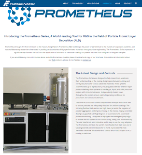
Forge Nano has just recently launched a new ALD Particle reactor for R&D including a vast range of goodies:
  • 8 precursor lines (gas, liquid, and solid precursor)
  • multiple fluidization aids
  • vibrating fluidized bed reactor
  • high shear jet assist the negation of powder aggregation and improve mixing in the reactor
  • mass spectrometer (MKS shown in picture)
  • hardware and software for control and in situ analysis of ALD coating in real-time
  • and more
[From Forge Nano] Prometheus brought fire from the Gods to the masses. Forge Nano’s Prometheus R&D tool brings the power of particle ALD to the masses of corporate, academic, and national laboratory researchers interested in pushing the boundaries of high-performance materials through surface engineering. The Prometheus Series represents a significant step forward for R&D into the application of sub-nano to nanoscale coatings on powder volumes from milligram to kilogram samples.

Screen dump from Forge Nano (LINK)

The Prometheus Series was designed to help researchers accelerate their understanding of the coating design space between existing and novel precursors and various substrate materials. These systems accommodate up to 8 precursors, including basic delivery and low vapor pressure delivery draw systems to handle gas, liquid, and solid precursor recipes with consummate ease. Independently-heated zones throughout the system ensure optimal operating conditions for precursors and sensitive substrates.

This novel ALD R&D tool comes complete with multiple fluidization aids to ensure particles are adequately fluidized for uniform coatings. The vibrating fluidized bed reactor and high shear jet assist the negation of powder aggregation and improve mixing in the reactor. Highly controlled dosing is supported with high degrees of automation and automated process monitoring. The system is equipped with emergency stop logic to enable the ALD system to run continuously, safely, and autonomously. The user interface is also is intuitive and is easy to use for easy adoption. The Prometheus Series is the world’s most flexible ALD R&D tool, and it was engineered with the researcher in mind. It provides the most advanced hardware and software for control and in situ analysis of ALD coating in real-time.

More infromatione : LINK

Isotropic Atomic Layer Etching of ZnO Using Acetylacetone and O2 Plasma

Plasma atomic layer etching (ALE) is typically know as an anisotropic etch method (directional), which is very useful property in many cases but sometimes not good at all, e.g, when you want to conformally (sorry for the reverse ALD expression) etch an high aspect ratio feature like a deep hole or a pillar.

Here is a fresh publication from TU Eindhoven and TNO/Holst Center in the Netherlands on their recent development of a Plasma ALE process capable of isotropical etch, i.e, conformal etching, of very high aspect ratio ZnO nanowires. Its is Open Access so go ahead and download it for free.

Fred, heel erg bedankt voor het delen van deze!

Isotropic Atomic Layer Etching of ZnO Using Acetylacetone and O2 Plasma

A. Mameli, M. A. Verheijen, A. J. M. Mackus, W. M. M. Kessels, and F. Roozeboom
ACS Appl. Mater. Interfaces, 2018, 10 (44), pp 38588–38595
DOI: 10.1021/acsami.8b12767
 
 
Atomic layer etching (ALE) provides Ångström-level control over material removal and holds potential for addressing the challenges in nanomanufacturing faced by conventional etching techniques. Recent research has led to the development of two main classes of ALE: ion-driven plasma processes yielding anisotropic (or directional) etch profiles and thermally driven processes for isotropic material removal. In this work, we extend the possibilities to obtain isotropic etching by introducing a plasma-based ALE process for ZnO which is radical-driven and utilizes acetylacetone (Hacac) and O2 plasma as reactants. In situ spectroscopic ellipsometry measurements indicate self-limiting half-reactions with etch rates ranging from 0.5 to 1.3 Å/cycle at temperatures between 100 and 250 °C. The ALE process was demonstrated on planar and three-dimensional substrates consisting of a regular array of semiconductor nanowires (NWs) conformally covered using atomic layer deposition of ZnO. Transmission electron microscopy studies conducted on the ZnO-covered NWs before and after ALE proved the isotropic nature and the damage-free characteristics of the process. In situ infrared spectroscopy measurements were used to elucidate the self-limiting nature of the ALE half-reactions and the reaction mechanism. During the Hacac etching reaction that is assumed to produce Zn(acac)2, carbonaceous species adsorbed on the ZnO surface are suggested as the cause of the self-limiting behavior. The subsequent O2 plasma step resets the surface for the next ALE cycle. High etch selectivities (∼80:1) over SiO2 and HfO2 were demonstrated. Preliminary results indicate that the etching process can be extended to other oxides such as Al2O3.

15 nm resolved patterns in Selective Area Atomic Layer Deposition

Here is an impressive and fundamental paper on selective area atomic layer deposition (SA-ALD)or just area selective deposition (ASD) that some prefer to call it.

The researchers at IBM has devleoped a bottom up approach on 300 mm pattern wafers that had been fabricated using standard trench first metal hardmask damascene scheme to create a line pattern of 36 nm pitch with single EUV exposures using low-k OMCTS 2.7 as the dielectric.
 
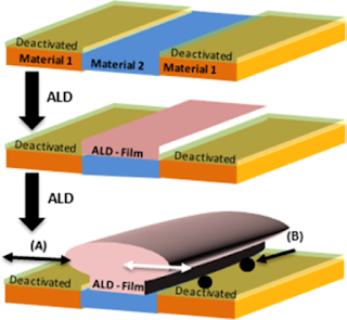
By deactivating ond surface with self-assembled monolayers (SAMs, Octadecylphosphonic acid) leaving another surface active for ALD processing (ZnO) they were able to produce 15 nm resolved patterns. One of the biggest challenges in the implementation of SA-ALD is the ability to maintain pattern fidelity and reduce defects during the ALD process (ZnO). 
 
Thank you Henrik Pedersen for sharing this paper!


Deactivating material is used to block one surface from ALD film growth. (A) ALD eventually leads to overgrowth of the film onto deactivated areas. (B) Defects in the deactivation layer can lead to the formation of locally deposited material. Published with permission from ACS Appl. Mater. Interfaces, 2018, 10 (44), pp 38630–38637 Copyright 2018 American Chemical Society.

Fifteen Nanometer Resolved Patterns in Selective Area Atomic Layer Deposition—Defectivity Reduction by Monolayer Design

Rudy Wojtecki, Magi Mettry, Noah F. Fine Nathel, Alexander Friz, Anuja De Silva, Noel Arellano, and Hosadurga Shobha
ACS Appl. Mater. Interfaces, 2018, 10 (44), pp 38630–38637
DOI: 10.1021/acsami.8b13896

Saturday, November 17, 2018

The new episode about ALDep is out - Area selective ALD with Gregory Parsons


Researchers from University of Groningen, the Netherlands confirm ferroelectricity in nanosized HfO2 crystals

Since the finding of ferroelectricity in HfO2 films of sub 10 nm thickness by Tim Böscke*,  (US8304823B2 NaMLab gGmbH) more then 10 years ago many leading R&D teams and semiconductor companies has confirmed the findings. Now also ferroelectricity in nanosized HfO2 crystalsby has been confirmed by the "Hafnia team” within the Nanostructures of Functional Oxides group, Zernike Institute for Advanced Materials, University of Groningen (UG), the Netherlands (LINK). 

* then at the DRAM Company Qimonda


Figure shows inside view of vacuum chamber in which the process of 'pulsed laser deposition' takes place, used to create the hafnium oxide crystals in this study. On the left the glowing substrate on which the film is growing with atomic control; in the center the blue plasma of ions that is created by shooting a laser on a target with the right chemical composition (target visible on the right side of the figure). | Photo Henk Bonder, University of Groningen


Ferroelectric materials have a spontaneous dipole moment which can point up or down. This means that they can be used to store information, just like magnetic bits on a hard disk. The advantage of ferroelectric bits is that they can be written at a low voltage and power. Magnetic bits require large currents to create a magnetic field for switching, and thus more power. However, according to the scientific community, the aligned dipoles in ferroelectric materials are only stable in fairly large groups; thus, shrinking the crystals results into the loss of dipole moment obstructing ferroelectricity based storage devices.

Nevertheless, eight years ago, the first publication by ex-Qimonda experts and researchers from Fraunhofer and RWTH Aachen (Appl. Phys. Lett. 99, 102903 (2011); https://doi.org/10.1063/1.3634052) announced that hafnium oxide thin films were ferroelectric when thinner than ten nanometres and that thicker films actually lost their ferroelectric properties. This triggered many groups across the globe to dig deeper and confirm the claim of researchers from NamLab. Noheda and her group at University of Groningen was also one of them. Since the ferroelectric hafnium oxide samples used in the study carried out at NaMLab were polycrystalline and showed multiple phases, obscuring any clear fundamental understanding of such an unconventional phenomenon, Noheda and her group decided to study these crystals by growing clean (single-phase) films on a substrate.

Using X-ray scattering and high-resolution electron microscopy techniques, the group observed that very thin films (under ten nanometres) grow in an entirely unexpected and previously unknown polar structure, which is necessary for ferroelectricity. Combining these observations with meticulous transport measurements, they confirmed that the material was indeed ferroelectric. Surprisingly, they noticed that the crystal structure changed when the layers exceeded 10 nm, thus reaching the same conclusion as of the Namlab.

In the substrate that UG researchers used, the atoms were a little bit closer than those in hafnium oxide which strained hafnium oxide crystals a little. Moreover, at a very small size, particles have a very large surface energy, creating pressures of up to 5 GPa in the crystal. This altogether forces a different crystal arrangement and in turn polar phase in the HfO2 film.

One contradicting finding of the UG researchers is that the HfO2 crystals do not need a ‘wake-up’ cycle to become ferroelectric. The thin films investigated at NamLab turned ferroelectric only after going through a number of switching cycles (wake-up cycles) needed to align the dipoles in “uncleaned” samples grown via other techniques. In case of the pulsed laser deposition setup and the substrate used at UG, the alignment is already present in the crystals.

Meanwhile, NaMLab has explored ferroelectric properties in atomic layer deposition (ALD) based thin-films of doped HfO2, and has achieved revolutionary results (LINK). A variety of dopant materials (Si, Al, Ge, Y, Gd, La and Sr) with a crystal radius ranging from 50 to 130 pm has been studied in addition to a mixed Hf1-xZrxO2. The aim is to develop a memory concept with the HfO2 based ferroelectric transistors (FeFET) as building blocks. The FeFET is a long-term contender for an ultra-fast, low-power and non-volatile memory technology. In these devices the information is stored as a polarization state of the gate dielectric and can be read non-destructively as a shift of the threshold voltage. The advantage of a FeFET memory compared to the Flash memory is its faster access times and much lower power consumption at high data rates. In the framework of a project together with GLOBALFOUNDRIES and Fraunhofer IPMS, which was funded by the Free State of Saxony, a one-transistor (1T) FeFET eNVM was successfully implemented at NaMLab in a 28 nm gate-first super low power (28SLP) CMOS technology platform using only two additional structural masks (LINK). The electrical baseline properties remain the same for the FeFET integration, demonstrating the feasibility of FeFET as low-cost eNVM.

Guest Blog by: Abhishekkumar Thakur, Fraunhofer IKTS / TU Dresden
Location: Dresden, Germany

LinkedIn: www.linkedin.com/in/abhishekkumar-thakur-16081991


ALD at SEMICON Europa 2018

This year was the first time in a long time that we did not organize an ALD Symposium at SEMICON Europa. We decided to keep it as a Dresden event and it will be held 10th of December (LINK) followed by a visit to the famous Dresden Christmas market..

This year, I was invited together with a number of other ALD people to present at the Materials session in the Tech Arena and there was a great program with impressive presentations chaired by Johan Dekoster from Imec.

Session

Materials Technology

Chair Johan Dekoster, Program Manager, imec
15:00 Introduction
15:05 New conductors – What are the options for N5, N3 and beyond?
Marleen van der Veen, Senior Scientist Nanointerconnects Metallization, imec
15:30 ALD/CVD applications, equipment and precursors in high volume manufacturing
Jonas Sundqvist, Group Leader, Fraunhofer IKTS
15:55 Advancing Atomic Layer Deposition and Atomic Layer Etching
Harm Knoops, Atomic Scale Segment Specialist, Oxford Instruments Plasma Technology
16:20 Atomic layer deposition for the synthesis and integration of 2D materials for nanoelectronics
Ageeth A. Bol, Associate Professor, Eindhoven University of Technology
16:45 Innovative Compound Semiconductor Based Engineered Substrates for Photonics, Power, Solar and RF Applications
Eric Guiot, Product Development Manager, Soitec
17:10 Kokusai Electric Corporation new products offering for 2018
Yoshio Kitahara, New Products offereing as Kokusai Electric, Kokusai Semiconductor Europe GmbH


Below here are some picture from the ALD Session, Exhibition and Show.


Heavy traffic on the Autobahn in to Munich - obviously more people are interested in ALD!

Friday, November 16, 2018

Beneq is expanding and looking for ALD professionals!

Beneq careers - come and join us at the Home of ALD

Join Us at Beneq!

The Beneq factory, the Home of ALD, is an extraordinary pool of thin film and display experience.
We strongly believe there is a thin solution for every challenge. And if somebody says it is impossible to do and others find the task too difficult, it only makes us more motivated. That is what Turning Innovations into Success is all about.

The future of Beneq is being built on the same character that defined the company.

Come and make Finnish high tech history with us! You can see the open positions below. You can also apply by sending us your open application and CV by clicking the link Open application below.

4th Area Selective Deposition (ASD) workshop April 4th – 5th, 2019 in IMEC

[Announcment LINK] ASM and IMEC are proud to announce that the 4th Area Selective Deposition (ASD) Workshop will be held on April 4th – 5th, 2019 in IMEC, Leuven (Belgium).

News tip by Henrik Pedersen - Tack så mycket


This workshop will bring together leading experts from both academia and industry to share their vision and results about: fundamental aspects of surface chemistry, new processes, metrology, fields of applications, technology needs and integration challenges for ASD. Based on a series of successful workshops at the North Carolina State University in 2018, Eindhoven University of Technology in 2017 and at IMEC in 2016, the two-days program will include invited and contributed speakers, a poster session and a reception on the evening of April 4th.
 

Tuesday, November 13, 2018

Spin Memory Teams With Applied Materials to Produce a Comprehensive Embedded MRAM Solution

FREMONT, Calif. — Spin Memory, Inc. (Spin Memory), the leading MRAM developer, today announced a commercial agreement with Applied Materials, Inc. (Applied) to create a comprehensive embedded MRAM solution. The solution brings together Applied’s industry-leading deposition and etch capabilities with Spin Memory’s MRAM process IP.


Key elements of the offering include Applied innovations in PVD and etch process technology, Spin Memory’s revolutionary Precessional Spin CurrentTM (PSCTM) structure (also known as the Spin Polarizer), and industry-leading perpendicular magnetic tunnel junction (pMTJ) technology from both companies. The solution is designed to allow customers to quickly bring up an embedded MRAM manufacturing module and start producing world-class MRAM-enabled products for both non-volatile (flash-like) and SRAM-replacement applications. Spin Memory intends to make the solution commercially available from 2019.

“In the AI and IoT era, the industry needs high-speed, area-efficient non-volatile memory like never before,” said Tom Sparkman, CEO at Spin Memory. “Through our collaboration with Applied Materials, we will bring the next generation of STT-MRAM to market and address this growing need for alternative memory solutions.”

“Our industry is driving a new wave of computing that will result in billions of sensors and a dramatic increase in data generation,” said Steve Ghanayem, senior vice president of New Markets and Alliances at Applied Materials. “As a result, we are seeing a renaissance in hardware innovation, from materials to systems, and we are excited to be teaming up with Spin Memory to help accelerate the availability of a new memory.”
About the PSC