Wednesday, March 14, 2018

RMD Dynasil employ CdTe ALD process for passivating HgCdTe IR sensors

Dynasil’s Radiation Monitoring Devices (RMD) is a world-renowned expert in the scintillation, photodetection, and radiation detection industries. At the recent Dynasil Corporation of America Annual Stockholder Meeting and Investor Presentation Conference Call it was reveiled that they have commericiallized an ALD process for passivating HgCdTe sensors with semiconductor-grade CdTe layer. The ALD coating is conformal, continuous and pinhole-free. Such low temperature CdTe ALD films have been previously published by Bengi Hanyaloglu et al (LINK).

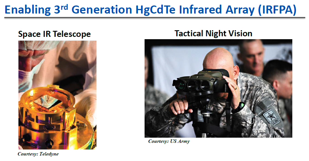
Applications for these sensors are for:
  • Space IR telescopes
  • Tactical night vision googles and binoculars etc.
Peter Sulick - Chairman, President & CEO has this to say about the application (Seeking Alpha call transcript LINK)

"Another exciting area for research that is going on at RMD is its activation of the mercaptal infrared arrays, third-generation infrared arrays, and as people in the optic suite are well aware, this mercaptal infrared arrays require stabilization on the surfaces because of the semiconductor bonds being open at the surfaces. And one of the ways to do that is through activation layer of mercaptal films, and RMD has developed a proprietary technology using atomic layer deposition to deposit this mercaptal films. And the important advantage that our technology brings is that these are controllable films, which can be deposited at much lower temperatures than currently thought, and that can have a big impact in the yield and in the utility of these infrared sensors. So we are excited about where this area is going."


RMD has developed an ALD process for passivating HgCdTe sensors with semiconductor-grade CdTe layer. The ALD coating is conformal, continuous and pinhole-free. (Dynasil 2018 Annual Meeting Management Presentation LINK


Recent metal oxide ALD publications in JVSTA for free download

Here is a list of recent ALD Papers published in JVSTA on the topic of metal oxides. The best of all The following articles are free to download for next 30 days!

Source: JVSTA News Letter


High-k oxides by atomic layer deposition - Applications in biology and medicine
Marek Godlewski, Sylwia Gierałtowska, Łukasz Wachnicki, Rafał Pietuszka, Bartłomiej S. Witkowski, Anna Słońska, Zdzisław Gajewski, and Michał M. Godlewski | Read More

Toward plasma enhanced atomic layer deposition of oxides on graphene: Understanding plasma effects
Christie J. Trimble, Trevor Van Engelhoven, Anna M. Zaniewski, Manpuneet K. Benipal, and Robert J. Nemanich | Read More
 
Al2O3/SiOnanolaminate for a gate oxide in a GaN-based MOS device
Daigo Kikuta (菊田大悟 ), Kenji Itoh (伊藤健治 ), Tetsuo Narita (成田哲生 ), and Tomohiko Mori (森朋彦 ) | Read More

Aluminum oxide/titanium dioxide nanolaminates grown by atomic layer deposition: Growth and mechanical properties
Oili M. E. Ylivaara, Lauri Kilpi, Xuwen Liu, Sakari Sintonen, Saima Ali, Mikko Laitinen, Jaakko Julin, Eero Haimi, Timo Sajavaara, Harri Lipsanen, Simo-Pekka Hannula, Helena Ronkainen, and Riikka L. Puurunen | Read More

Atomic layer deposition of tin oxide thin films from bis[bis(trimethylsilyl)amino]tin(II) with ozone and water
Jere Tupala, Marianna Kemell, Miika Mattinen, Kristoffer Meinander, Sanni Seppälä, Timo Hatanpää, Jyrki Räisänen, Mikko Ritala and Markku Leskelä | Read More

Atomic layer deposition of molybdenum oxide using bis(tert-butylimido)bis(dimethylamido) molybdenum
Adam Bertuch, Ganesh Sundaram, Mark Saly, Daniel Moser, and Ravi Kanjolia | Read More

Spatial atomic layer deposition on flexible porous substrates: ZnO on anodic aluminum oxide films and Al2O3 on Li ion battery electrodes
Kashish Sharma, Dmitri Routkevitch, Natalia Varaksa, and and Steven M. George | Read More

Come meet the German ALD Industry next week in Dresden - everybody will be there!

A topical workshop with focus on industrialization and commercialization of ALD for current and emerging markets

Atomic Layer Deposition (ALD) is used to deposit ultrathin and highly conformal thin films. ALD is unique in the sense that it employs sequential self-limiting surface reactions for growth in the monolayer thickness regime. According to market estimates the equipment market alone is currently at an annual revenue of US$ 1.5 - 1.7 billion (2017) and it is expected to double in the next 4-5 years.

In a European context ALD was invented independently twice in Europe (Russia & Finland) and since the last 15 years Germany has grown to become one of the strongest European markets for ALD in R&D, chemicals, equipment and end users. Here, Dresden and Saxony isa unique ALD hotspot due to a strong semiconductor and equipment industry.

The Event will focus on the current markets for ALD, besides the leading edge semiconductor industry, applications in MEMS and Sensors, Display, Lightning, Barriers and Energy Devices will be addressed.


Location: HYPERION Hotel Dresden am Schloss, Dresden (Deutschland)

Program: LINK

Regsitration: LINK


Tuesday, March 13, 2018

Thermal ALD of aluminum metal at low temperature

Aluminum metal is important in semiconductor devices and as a metal itself in metallization and as an alloy in e.g. TiAl metal gates or TiAlN electrodes. Prof. Winter and his team at Wayne State have previously published new paths to thermal ALD of titanium, here they published their recent achievement for thermal ALD of aluminum!

Atomic Layer Deposition of Aluminum Metal Films Using a Thermally Stable Aluminum Hydride Reducing Agent

Kyle J Blakeney and Charles H. Winter
Chem. Mater., Just Accepted Manuscript

The thermal atomic layer deposition of aluminum metal films at temperatures as low as 100 °C is described using AlCl3 and a new aluminum dihydride complex that is supported by a bulky amido-amine ligand. A growth rate of about 3.5 Å/cycle was observed within a 120-160 °C ALD window and self-limiting growth was established for both precursors. Resistivities as low as 3.03 Ω·cm were obtained for the aluminum metal films. Root mean square surface roughnesses were 19-23% of the film thicknesses, as determined by atomic force microscopy. Films grown on TiN substrates were crystalline by X-ray diffraction. X-ray photoelectron spectroscopy of films grown at 100 and 140 °C showed Al (> 94 at%) with C and Cl impurities below the detection limit (< 1 and 0.5 at%, respectively). Accordingly, this process affords high purity, low resistivity aluminum metal films.


SoLayTec ships new ALD order to Asia for PERC cell manufacturing

North American Clean Energy reports (LINK): Amtech Systems, Inc. (NASDAQ: ASYS), a global supplier of production equipment and related supplies for the solar, semiconductor, and LED markets, announced its solar subsidiary, SoLayTec B.V., has shipped a next generation solar Atomic Layer Deposition (ALD) to an Asian customer. While the PV market is shifting towards high efficiency cell designs, production with high yield, A-grade cells, is getting increasingly important. 
 

Fokko Pentinga, CEO and President of Amtech, commented, "For this project we are delivering the equipment for the PERC line upgrade and assisting the customer with the PERC ramp-up and line integration. PV manufacturers are experiencing extreme price pressure, resulting in an increasing need for higher cell quality with narrow cell efficiency distribution. The highest line yield possible of A-grade cells is essential to ensure good margins for these advanced production lines. Al2O3 wrap-around during deposition will result in reduction of the cell efficiency by as much as 0.2%, as well as front side color variations. Our ALD equipment addresses PV manufacturers' challenges, by delivering the highest PERC cell efficiency using Al2O3,, highest A-grade cells, and stable deposition process without any wrap around. Another challenge we address for A-grade cells is scratch free manufacturing of SiNx deposition for rear-side capping and front-side ARC. Our scratch free solution using our direct-plasma PECVD equipment is gaining momentum, with shipments and order backlog totaling more than 1GW."

Wednesday, March 7, 2018

NCD Contracted with Risen Energy to supply 1.8GW solar cell ALD equipment

NCD recently signed the largest contract with Risen Energy, a Chinese solar cell manufacturer, to provide ALD equipment in the next six months. This agreement is to supply 1.8GW solar cell manufacturing equipment, so it indicates that the superiority and reliability of NCD’s ALD equipment has been fully proven to the customer.

This system is (Lucida GS Series + Automation), the main product of NCD's solar division, to increase the efficiency of solar cells by depositing high quality Al2O3 ALD thin films. Lucida GS Series is batch type ALD deposition equipment that forms backside passivation of Al2O3 on multiple wafers and can process more than 4.500 wafers (@ 4nm thickness) of 156mm x 156mm size per an hour. By applying Lucida GS Series in the production of solar cells, customers can dramatically lower the production cost of high efficiency solar cells due to the high-volume productivity, high yield, efficient gas consumption and low maintenance cost compared to competitors.

Lucida GS Series has become the first choice for ALD process in high efficiency solar cell manufacturing, based on its advantages and excellence. NCD expects to record the best sales by the rapid sales growth in the solar sector in 2018. 


(Lucida GS Series + Automation)

Tuesday, March 6, 2018

Training School on the Chemistry of ALD 19 and 20 march in Luxembourg

HERALD COST action (MP1402: Hooking together European research in Atomic Layer Deposition) and MASSENA doctoral program (Materials for Sensing and Energy harvesting) co-organize a Training School entitled “Chemistry of Atomic Layer Deposition” (https://www.list.lu/en/event/belux3/ ) the 19 and 20 march in Luxembourg.

Experts from ALD-complementary fields animate a two days’ interactive training school about aspects associated with the chemistry behind the ALD process.
The following aspects will be addressed:
1-ALD opportunities and challenges by Dr. Elisabeth Blanquet, Univ. Grenoble Alps, Research Director, SIMAP, France
2- Precursor design and its impact on the ALD chemistry and kinetics  by Dr. Jean-Marc Girard, CTO and Head of R&D at Air Liquide Advanced Materials, France
3- Modelling aspects and tools by Dr. Alain Estève, Research Director, Head of NEO group “Nano-Engineering and integration of metal-Oxide-based nanostructures and their interfaces” LAAS-CNRS, France
4- In situ investigation of the ALD process by Dr. Martin Knaut, Institute of Semiconductors and Microsystems, Dresden, Germany
5- Approaches for area-selective ALD by Dr. Christophe Vallée, CEA – LETI - MINATEC, Grenoble, France. Head of the material department of Polytech Grenoble, Professor at Grenoble Alpes University and at Tsukuba University (Japan).
 

Limited number of travel grants (650 €/participant) will be given upon evaluation of applications. Participation from ITC countries is strongly encouraged. Thank you to inform us of your application in the registration form.

COST Action MP1402 - HERALD
Hooking together European research in Atomic Layer Deposition

Monday, March 5, 2018

ISAC Research - South Korean ALD OEM

Today I came across a South Korean ALD OEM that I have not descovered previously. Possibly this company is well knwon elsewhere - ISAC Research. According to their web they supply a full range of ALD equipment covering all wafer sizes up to 300 mm, batch processing for CIGS and also powder processing.
  •  
  •  
  •  
  •  
  •  


SEMICONDUCTOR  
  • Patterning spacer (SiO, SiON, SiOC, SiN)  
  • Gate high-k (HfO)
  • Capacitor high-k (ZrO)
  • Diffusion barrier (TiN,TaN)
OLED
  • Moisture barrier (AlO)
  • ITO etching barrier (AlO)
  • Transparent conducting oxide (ZnO, Al:MgO, SnMgO)
PV
  • AlO passivation for c-Si solar cell
  • ZnOS buffer layer for CIGS thin film solar cell
MEMS/NEMS

Powder

  • ALD coating on micro- and nanosized particles (Pt, Ru)
  • Functional coating
Flexible
  • LiBS coating (AlO)
  • Moisture barrier (AlO)
Surface protection
  • Anti-corrosion coatings for metal


Beneq Roll-to-roll for continuous ALD film deposition

Roll-to-roll for cost-effective ALD

[From Beneq Blog] The implementation of roll-to-roll is important for cost-effective ALD in several areas. One of the most important applications areas is ALD coatings as barriers for polymer substrates. The barrier films are critical for encapsulation and moisture barrier protection for flexible organic light emitting diodes (OLED) displays and thin film solar cells.

Internal Beneq results confirmed by independent laboratories have shown that Al2O3 ALD coatings using TMA and ozone form excellent gas barriers with WVTR values of about 1x10⁻⁵ g/m2/ at 38C/85% relative humidity.

Beneq WCS 600

The Beneq WCS 600 is the ideal option for customers looking for a large and cost-effective ALD roll-to-roll system. Typical non-uniformities are less than 2% across the web width for a typical Al2O3 coating.  A WVTR of 10-4 g/m2 day can be expected at a web speed of 0.25 meters/minute.

The Beneq WCS 600 a large and cost effective ALD roll-to-roll system (Beneq.com)
 
 
Learn more

EQP for the analysis of positive and negative ions, neutrals, and radicals from plasma processes

The Hiden Analytical EQP system is a combined mass spectrometer and energy analyser for the analysis plasma ions, neutrals and neutral radicals. The EQP instrument includes operating modes for positive ion, and negative ion analysis. Threshold ionization and electron attachment ionization modes are available for detailed neutral radical studies, for analysis of both electro-positive and electro-negative plasma radicals.

EQP Product page : LINK


The EQP system is now available with integrated MCS – multi channel scalar data acquisition with time resolution to 50 nano seconds providing for fast data acquisition in pulsed plasma applications.


Understanding ALD, MLD and SAMs as they enter the fab


[Solid State Technology LINK]As the world of advanced manufacturing enters the sub-nanometer scale era, it is clear that ALD, MLD and SAM represent viable options for delivering the required few-atoms-thick layers required with uniformity, conformality, and purity.

BY BARRY ARKLES, JONATHAN GOFF, Gelest Inc., Morrisville PA; ALAIN E. KALOYEROS, SUNY Polytechnic Institute, Albany, NY

Device and system technologies across several industries are on the verge of entering the sub-nanometer scale regime. This regime requires processing techniques that enable exceptional atomic level control of the thickness, uniformity, and morphology of the exceedingly thin (as thin as a few atomic layers) film structures required to form such devices and systems.[1]


 Full article : Solid State Technology LINK

Friday, March 2, 2018

Call for Abstracts - 3rd Area Selective Deposition Workshop (ASD 2018)

Call for Abstracts
Extended to March 5, 2018
The principal chemical processes and mechanisms that enable Area Selective Deposition (ASD) are rapidly becoming critical in several areas of materials and technological advancement. Most notably, the semiconductor industry will likely need new ASD processes to enable “chemical alignment” to complement traditional physical alignment (i.e. lithography) to allow transistors to scale to less than 10 nm dimensions. Other fields are also exploring chemical selectivity in materials to achieve precise targeted performance. Catalytic materials, for example, which are commonly employed to promote chemically selective reactions, are now being designed and constructed using site-selective deposition reactions. In addition, the growing complexity of energy generation and storage materials are also driving the need for new site- or area-selective processes to control heterogeneous material structures.

To share advances in these areas, the 3rd Area Selective Deposition Workshop (ASD 2018), will be held on April 29 – May 1, 2018, at North Carolina State University in Raleigh North Carolina USA. The Workshop will bring together leading international scientists and engineers from academia and industry from all regions to share results and insights into: 1) fundamental principles and barriers to area selective deposition; 2) technological needs and challenges of ASD; 3) new chemical approaches and processes to address the expanding needs; and 4) surface characterization techniques and metrology innovation for ASD.

Based on successful workshops at the Eindhoven University of Technology in 2017 and at IMEC in Leuven Belgium in 2016, ASD 2018 will consist of two days of presentations and discussions, preceded by a welcome reception at North Carolina State University on April 29. The program will include a series of invited and contributed speakers, a panel discussion, as well as a poster session reception on the evening of April 30.
Topics:
  • Chemical selectivity in surface reactions
  • Mechanisms and surface-dependent thin film nucleation and growth
  • Surface passivation for controlled nucleation and growth
  • Patterned deposition resists, including organic monolayers, for selective deposition
  • Chemical activation for nucleation enhancement
  • Selectivity in thin film etching, including atomic layer etching (ALE)
  • Processes and mechanisms for area-selective chemical vapor deposition (CVD)
  • Processes and mechanisms area-selective atomic layer deposition (ALD)
  • Metrology for Area-Selective Deposition
  • Applications for area-selective deposition in electronics manufacturing
  • Applications for area-selective processing in catalysis, energy generation and storage, and other emerging areas
  • Surface characterization techniques for defects formation and mitigation
Invited:
  • Rohan Akolkar, Case Western University, USA
  • Silvia Armini, IMEC, Belgium
  • Sean Barry, Carlton University, Canada
  • Yves Chabal, University of Texas, Dallas, USA
  • Steve George, University of Colorado at Boulder, USA
  • Jessica Kachian, Applied Materials, USA
  • Joerg Lahann, University of Michigan, USA
  • Junling Lu, University of Science & Technology of China, China
  • Adrie Makus, Eindhoven Technical University, The Netherlands
  • Chuck Winter, Wayne State University, USA

Panel Discussion:
As area selective deposition becomes critical for multiple uses, loss of selectivity and defect formation continue to be obstacles to practical implementation. New surface characterization and metrologies are needed for better mechanistic understanding of defect formation and mitigation. This panel will bring experts from academia, industry and consortia to discuss these challenges and potential solution paths.
Key Deadlines:
Abstract Submission Deadline Extended to: March 5, 2018
Author Acceptance Notifications: March 26, 2018
Early Registration Deadline: April 6, 2018
Hotel Reservation Deadline: April 6, 2018

Program Chair

Gregory Parsons
North Carolina, State Univ., USA
Organizing Committee

Adrie Mackus
Eindhoven University of Technology,
The Netherlands (ASD 2017 Chair)

Annelies Delabie
IMEC, Belgium (ASD 2016 Chair)

Dennis Hausmann
Lam Research, USA


AVS | 125 Maiden Lane, 15th Floor, New York, NY 10038