%20(1).png)
According to the new report, “Atomic Layer Deposition Market - By Type (Equipment & Materials); By Application (Gate Dielectrics, Gate Electrodes, Metal Interconnects, Diffusion Barriers, Memory Chips, Multilayer Capacitors, OLED Layers, Solar Cells, Fuel Cells, MEMS and Others); By Geography – Forecast (2016-2022)”, published by IndustryARC, the atomic layer deposition market to cross USD 5 Billion by 2022 at a high CAGR.

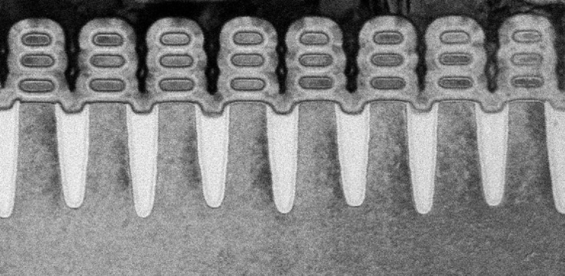
Atomic Layer Deposition in increasingly being used in manufacturing of electronic products where thickness of the film is absolutely imperative such as; smart phones, printers, data storage devices, displays, different types of small electronic components and many others products. It is mainly responsible for semiconductor fabrication and nanomaterial synthesis. Growing application of thin film coatings is the major driving factor for atomic layer deposition market. Through atomic layer deposition, ultra-thin films can be created in a sequential and self-limiting way depending on the material or product, which needs the layer to be applied on. Atomic layer Deposition process is especially favored because of its ability to control the film thickness in nanometer thickness regime. Atomic layer deposition is a perfect deposition method for applications where the surface area of the base material is very small.
According to a recent study from IndustryARC the global market value of atomic layer deposition was $910 million in 2015. Atomic layer deposition instruments are expensive as compared to conventional techniques such as MOCVD and PVD, consequently the equipment used for atomic layer deposition accounted for more than 60% of the global market revenue share.
Inquiry before Buying Report @ http://www.industryarc.com/inquiry-before-buying.php?id=15340