Wednesday, January 4, 2017

Rasirc to present New ALD chemistries for low temperature oxide and nitride films at ALD4Industry

We are very happy to announce that have received a late news abstract from RASIRC out of San Diego, USA, for a presentation to be given at the EFDS Workshop "ALD for Industry" entitled New ALD chemistries for low temperature oxide and nitride films”. RASIRC is also sponsoring the workshop and will have a stand the the exhibition.

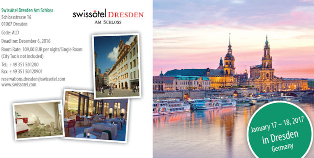
There are still room for some delegates to attend - so please consider to come to Dresden 17-18th of January and participate!


I have met Rasirc many times in Dresden and around the world. Here is a picture from Rasirc sponsoring and presenting the CMC Conference 2016 in Hillsboro USA organized by TECHCET, "Hydrazine as a Low Temperature Nitride Source: Materials Challenges for High Volume Manufacturing " at the event posing Dan Alvarez CTO and Jeff Spiegelman President and Founder.

Link to ALD fro Industry Program HERE

#ALD4Industry (follow in Twitter)

In an European context ALD was invented independently twice in Europe (Russia & Finland) and since the last 15 years Germany has grown to become one of the strongest European markets for ALD in R&D, chemicals, equipment and end users. Here, Dresden and Saxony is a unique ALD hotspot due to a strong semiconductor and equipment industry.  
 
As you can see we have managed to put together a fantastic program with 
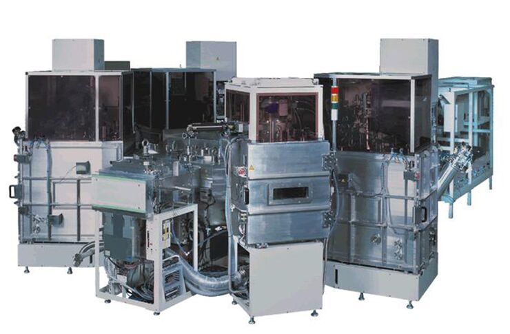
representatives from the European ALD Equipment Industry : Picosun (FIN), Beneq (FIN), Sentech (GER), FHR Anlagenbau (GER), Encapsulix (FRA), ASM International (NL) and special guests from the USA  - Ultratech CNT! 
 
In addition, representatives from the chemical industry (Air Liquide), customers (Robert Bosch) and research institutions from Germany (Fraunhofer) and Finland (Aalto University and VTT Finland) will make invited and contributing talks. Topics will cover industrialization of ALD beyond the semiconductor industry:
 
▪ MEMS & Sensors ▪ Display ▪ Lightning ▪ Barriers ▪ Photovoltaics

Please visit EFDS for all information for this event and how to register HERE!


Platinum Sponsors:

logo_picosun
logo_beneqlogo_asm
logo_air-liquide

logo_fhr


Gold Sponsors:

logo_leskerlogo_strem-chemicals
logo_pegasuslogo_sentechlogo_modularflow
logo_rasirclogo_eurislogo_ultratech-cntlogo_cs-cleanlogo_ebera

Tuesday, January 3, 2017

AUO introduced bi-directional foldable AMOLED display with less than 4 mm folding radius

OLED Net reports: Taiwanese company, AU Optronics(AUO) introduced bi-directional foldable AMOLED display at IDW(International Display Workshoops) 2016 opened in Japan Fukuoka from last December 7th through 9th, which both internal and external displays can be bent 180 degrees.

The Display has an impressivily small folding radius of less than 4 mm and can endure folding cycle of more than 1.2 million times. There are no reports yet of which encapsulation technology that has been employed.

Monday, January 2, 2017

Safe garnet-based solid-state Li metal batteries using conformal ALD

COLLEGE PARK, Md. — A team of researchers at the University of Maryland Energy Research Center and A. James Clark School of Engineering have announced a transformative development in the race to produce batteries that are at once safe, powerful, and affordable. 


The researchers are developing game-changing solid-state battery technology, and have made a key advance by inserting a layer of ultra-thin aluminum oxide between lithium electrodes and a solid non-flammable ceramic electrolyte known as garnet. Prior to this advance, there had been little success in developing high-performance, garnet-based solid-state batteries, because the high impedance, more commonly called resistance, between the garnet electrolyte and electrode materials limited the flow of energy or current, dramatically decreasing the battery's ability to charge and discharge.

The University of Maryland team has solved the problem of high impedance between the garnet electrolyte and electrode materials with the layer of ultrathin aluminum oxide, which decreases the impedance 300 fold. This virtually eliminates the barrier to electricity flow within the battery, allowing for efficient charging and discharging of the stored energy.

A new paper describing the research was published online December 19 in the peer-reviewed journal Nature Materials.

“This is a revolutionary advancement in the field of solid-state batteries—particularly in light of recent battery fires, from Boeing 787s to hoverboards to Samsung smartphones,” said Liangbing Hu, associate professor of materials science and engineering and one of the corresponding authors of the paper. “Our garnet-based solid-state battery is a triple threat, solving the typical problems that trouble existing lithium-ion batteries: safety, performance, and cost.”

LEGO-style nanolayer self assembly for future logic and memory devices


Self-assembly of molecules that spontaneously form ordered phases exhibiting well-defined nanoscale periodicity and shapes may be used for future Logic, Memory and intreconnects. However, until to day these have been limited to lamellae or hexagonally packed cylinders.

A team of researchers at Brookhaven National Laboratory have recently showed how soft self-assembling materials—block copolymer thin films—can be manipulated to form a diverse library of previously unreported morphologies. The processes s modules can be repeated as an iterative self-assembly as described in the figure below.

You can read all about these exciting results it in the Open Source publication in Nature Communications: Rahman, A. et al. Non-native three-dimensional blockcopolymer morphologies. Nat. Commun. 7, 13988 doi: 10.1038/ncomms13988 (2016). 

(a) The responsive assembly strategy begins by depositing a neutral brush on the substrate of interest. A block copolymer (BCP) film is then spin-coated on the substrate and annealed to yield a well-defined morphology. Selective infiltration synthesis (SIS) is used to load one of the BCP domains with alumina; this process ‘fixes’ the thin film, making it robust and insoluble, and generates height variation between the domains. The fixed BCP film can be used as the substrate in a subsequent round of ordering. The height variation (which remains after depositing the neutral brush) templates the subsequent BCP layer, causing it to align and register in a well-defined way. Single-layer, bi-layer or multilayer inorganic replicas can be formed by ashing the film (exposure to O2 plasma), as shown in the right-most column. (b) Cross-sectional scanning electron microscopy (SEM) of an exemplar single-layer infiltrated nanostructure before and after ashing (lamellar-forming BCP, L36). (c) Cross-sectional SEM of an exemplar four-layer nanostructure. False-colour applied to highlight layers (from bottom to top): L104, L74, L36, C132. Scale bars are 100 nm. Released unde Creative Commons 4.0 from Rahman, A. et al. Non-native three-dimensional blockcopolymer morphologies. Nat. Commun. 7, 13988 doi: 10.1038/ncomms13988 (2016). 

Gallium nitride thin-film transistors produced in 200°C process by hollow cathode PEALD

Hollow cathode plasma sources, are an alternative to ICP and CCP sources and has been successfully introduced for PEALD by Meaglow Ltd. Semiconductor Today reports: Bilkent University in Turkey has developed a low-temperature process to create gallium nitride (GaN) back-gated thin-film transistors (TFTs) on flexible and rigid substrates [S. Bolat et al, Appl. Phys. Lett., vol 109, p233504, 2016]. The team reports that the "overall fabrication thermal budget is below 200°C, the lowest reported for the GaN-based transistors so far." 

According to the article in Applied Physics Letters, the GaN thin films were grown by hollow cathode plasma assisted atomic layer deposition (HCPA-ALD) at 200 °C using the popular Ultratech Cambridge Nantech Fiji PEALD system equipped with an HCP source from Meaglow. 

More information on can be found here:


Wednesday, December 28, 2016

Picosun sweeps through China with over 20 new customers

ESPOO, Finland, 28th December, 2016 – Picosun Oy, the leading supplier of advanced industrial ALD (Atomic Layer Deposition) solutions, reports winning more than 20 new customers in China for its ALD systems since December 2015.


According to SEMI, out of 62 front-end fabs that will open worldwide over the next three years, 26 are in China, representing 42% of the global total. (Data from SEMI)

Amongst these customers are many of China’s leading companies in LEDs, III-V semiconductors, and new energy. Thanks to the high technical level of PICOSUN™ ALD equipment and the excellent customer support, Picosun has become the supplier of choice for ALD technology in China.

Chinese semiconductor manufacturing and the number of planned fabs in the country are booming, making China the new key market for semiconductor processing equipment. This is the most excellent news considering Picosun’s prominent position as the advanced ALD solutions provider. Collaboration with the leading Chinese research institutes is further supporting Picosun’s sprint in the market.

“We are extremely happy with the development of our ALD business in China. Our achievements are based on solid ALD knowhow, high-level support and proprietary designs, which give the best value for our Chinese customers and ensure our steady progress in the Chinese market. We are committed to our customer satisfaction by providing the newest and the best ALD solutions and systems in the market,” states Mr. Xiaopeng Wu, CEO of Picosun China.

Thursday, December 22, 2016

Applied Materials reportedly missing out on ALD for OLED encapsulation

Applied Materials is world leading in CVD processing for wafer and display. However, i big part of the CVD equipment market today is the booming segment of ALD where Applied only have single digit percentage of the revenue. According to a recent report by Seeking Alpha, "Applied Materials is facing strong competition as its deposition technology is being supplanted by Atomic Layer Deposition at Samsung Electronics and LG Display". Other applications where Applied Materials did not enter with ALD include:
  • DRAM High-k MIM Capacitors
  • Logic High-k Metal Gate Stack 
  • Double Patterning 
However, Applied Materials has reported strong revenue in Selective Etch and Olympa ALD (>USD 230M) Possibly they have some advanced Spatial ALD technology up the sleeve also for OLED encapsulation.

 Watch For Big Display Equipment Cancellations Coming From Applied Materials

  • Tight supply of a critical piece of OLED equipment from Canon Tokki will limit OLED production in 2017 and impact Applied Material's sales of supplemental equipment.
  • Applied Materials also is facing strong competition as its deposition technology is being supplanted by Atomic Layer Deposition at Samsung Electronics and LG Display.
  • As much as $1 billion in display equipment from Applied Materials could be cancelled in 2017.
Full report

More details on the Canone Tokki and Apple OLED roll out story here from Bloomberg:

Apple's Search for Better iPhone Screens Leads to Japan's Rice Fields [Bloomberg TV]

The ELVESS OLED mass production system. Source: Canon Tokki Corp.


ALD for Industry Get toghether at Freiberger Schankhaus 17 January 2017

The ALD for Industry workshop is coming up in Dresden 17-18th of January 2017 organizes by EFDS and ALD Lab Saxony - IHM TU Dresden & Frauhhofer IKTS with support from NaMLab, von Ardenne and Globalfoundries and very many sponsors from the ALD industry!

Frohe Weihnachten und ein gusundes Neues Jahr aus Dresden


On the first day after the tutorials there will be an opportunity to visit ALD labs and cleanrooms and labs at the Technical University Dresden and Fraunhofer Institute for Ceramic Technologies and Systems IKTS. After the tours we will have a get to gether "ALD Fest" at Freiberger Schankhaus in Dresden Altstadt. Her you can read about the History of this former Pharmacy starting in 1756 under the intriguing original name  »Zum König Salomon« (The King Solomon) : LINK


Platinum Sponsors:

logo_picosun
logo_beneqlogo_asm
logo_air-liquide

logo_fhr


Gold Sponsors:

logo_leskerlogo_strem-chemicals
logo_pegasuslogo_sentechlogo_modularflow
logo_rasirclogo_eurislogo_ultratech-cntlogo_cs-cleanlogo_ebera


Wednesday, December 21, 2016

Beneq reports on record-breaking black silicon solar cells


Beneq reports that their equipment has been used in the creation of record-breaking black silicon solar cells, and we have over the years been involved in many projects developing high power solar cells. Lately, we have been working mostly with rear surface passivation of solar cells.

PERC solar cells are a type of high efficiency solar cells where the electron gain of the cell is improved with a passivating film on the rear side of the cell structure. The complete term is Passivated Emitter Rear Cell. The PERC manufacturing technology has become more mature and cost effective, and PERC cells are now causing a buzz in the industry.
In a recent article, 20.8% industrial PERC solar cell: ALD Al2O3 rear surface passivation, efficiency loss mechanisms analysis and roadmap to 24%, which was published in Solar Energy Materials and Solar Cells, the authors present a cost-efficient PERC roadmap at industrial level. In the paper, key processes of ozone based ALD Al2O3 rear surface passivation are presented, resulting in 20.8% PERC cells made with an industrial process. The equipment used in the study was Beneq’s P800 industrial ALD reactor. 

Full Story in Beneq Blog: LINK

Beneq is looking for talent to strengthen their ALD sales in USA, UK and Finland


Beneq is a leading supplier of Atomic Layer Deposition (ALD) equipment and thin film coating services. Beneq equipment and thin film experience is used for example for improving the performance and durability of electronics, optics and solar cells, and protecting materials humidity and corrosion, as well as in many emerging thin film applications.

We employ a wide range of professionals as well as work tightly with for example sales agents and distributors. We offer a possibility to be part of an ambitious team of professionals and a chance to work in a company doing truly international business. At Beneq you can utilize your competences and learn more every day! 

Currently we are especially interested in finding talent to strengthen our ALD sales: 

To get more information and to apply, please visit Beneq Careers http://beneq.com/careers.html

Tuesday, December 20, 2016

NCD enables ALD decorative coatings with high productivity and low expense

Usually, most of people want to make their costly articles and valuable electric devices more unique and more outstanding. In order to meet these requirements, ALD technology could provide goods with higher quality and more functions like anti-tarnishing, anti-wear and anti-biotic effects as well as more conspicuous colors by thin film interference phenomena. NCD, a next generation technology leader of solar cell, display and semiconductor manufacturing systems, demonstrated several precise color coatings on various samples with multi laminating metal oxide thin films prepared by atomic layer deposition. 
Various color coating simulations using Essential Macleod software

The Essential Macleod software was used to estimate various color coating results, and most full visible range of colors could be obtained by controlling thicknesses of metal oxides with their light interferences and reflections. The various structures of five nano-laminated thin films of Al2O3 and TiO2 were designed in advance and the evaluated colors corresponded well with the simulated color spectrum results.

Various ALD decorative color coatings on watch bands


Different colors on the back cover of a smart phone by ALD (a) with incident angles at 0° and (b) with incident angle at 90°

The parts of a watch band that were coated at a low growth temperature of 100°C using Lucida series ALD, show different, bright, warm, metallic and mirror-like colors of purple, blue, green, yellow, orange and red, that are presenting nearly full rainbow colors.


Video of the decorative color coating on the back cover of a smart phone by ALD

The back cover of a smart phone deposited by ALD shows the decorative red color with incident angles at 0° and gold one with incident angle at 90°. Also the colors are changed with various view angles, because the relative thicknesses of the layers are varied with the incident angles of light and then the light waves traveling through the thicknesses characterize their own colors matching the wave lengths.

ALD technology is a great method to provide various functions like anti-tarnishing, anti-wear and anti-bacterial effects as well as tailed decorative coatings on very complicated figures like 3D objects at low temperatures and the dominant film quality without particles and pinholes and also the application of ALD decorative coating has huge markets such as automotive, electronics, jewelry, medical device, sporting goods, watch and other advanced coating products. Even though there are these many advantages and potentials of ALD decorative coatings, ALD technology has not been well industrialized until now because of its low productivity and high product cost. However, NCD has developed the highest throughput and the largest-area ALD technology such as Lucida GS and GD Series ALD, so enables to easily provide remarkable ALD systems for economic decorative mass production coatings for customers who want to make their products to be outstanding and different.

Previous news from NCD


Aug 31, 2016 ... NCD reports today (8/31 2016) :The OLED market is going to prospect fast gigantic growing in the near future because OLED has the ...
Mar 28, 2016 ... As announced some weeks ago I am happy to have NCD as sponsor for the BALD Engineering ALD News blog. Here a review of the company ...
Dec 12, 2015 ... "NCD has recently contracted with HYUNDAI HEAVY INDUSTRIES(HHI) to supply 200MW of solar cell manufacture equipment which would be ...
Jul 21, 2016 ... NCD has just contracted with Chinese DMEGC to supply solar cell manufacturing equipment which would produces over 100MW.

Aug 9, 2016 ... NCD CO., LTD. NCD CO., LTD .... NCD to deliver Lucida GD series ALD system for OLE... Ultra-High Aspect Ratio InP Junctionless FinFETs b.
 
Apr 12, 2016 ... Check out the video in the supplemntary information linked below! The Al2O3 was deposited using a LUCIDA D100 ALD reactor form NCD.

Monday, December 19, 2016

Registration EuroCVD-Baltic ALD 2017 in Sweden

Registartion Opens 2 January 2017 and the registration fee includes admission to the conference Monday 12 June to Wednesday 14 June, conference material, lunch, coffee/tea breaks, welcome mixer Sunday 11 June, pub night on Monday 12 June and conference dinner on Tuesday 13 June.


Please find all details here: LINK

Accomidation for pre-booked Hotels are available here: LINK

Abstract Deadline is 10 January 2017


Umicore's pioneering approach to ethical cobalt sourcing for CVD/ALD precursors

Cobalt is one of the most  important metals for leading edge BEOL Copper interconnects used for the processor chips in Smartphones, Tablets, PCs and Servers. In a modern highly scaled copper interconnect there are numerous opportunities for electromigration (EM) failure in the narrow copper lines, starting at line edges, at contact and via interfaces, and at CMP damaged surfaces. In addition, since grain growth is retarded in the smaller lines grain boundaries are becoming an increasingly significant electromigration failure mode. The focus is on very thin barriers that also act to inhibit EM at surfaces as well as alloy additions that can improve grain boundary EM. Of course, there are always tradeoffs, e.g. alloying the copper with something like Mn improves EM, but results in higher RS. Co as barrier and cap may also improve EM. Introduction of a Co liner and selective cobalt capping layer has demonstrated improved copper gap fill and an order-of-magnitude reduction in electromigration.  [TECHCET ALD/CVD Metal precursor report]

More details on the introduction of Co for Cu BEOL can be found in this article by Applied Materials published in Semicondtuctor Engineering [LINK].


According to news released by Umicore: Umicore is the first company in the world to have introduced a Sustainable Procurement Framework for Cobalt and is the first to obtain external validation for its ethical procurement approach in this area. It aims to minimize the risk of any connection between the cobalt in its supply chain – and subsequently that of its customers – and human rights abuses or unethical business practices. The framework builds on the specific approach to sustainable and ethical cobalt sourcing that Umicore introduced in 2004. Since then it has evolved to address specific risks linked to unethical mining practices, such as child labour and poor health and safety conditions. 

For CVD/ALD Umicore is offering two of the most used cobalt precursors within the  Sustainable Procurement Framework for Cobalt :

CCTBA : Hexacarbonyl(3,3-dimethyl-1-butyne)dicobalt [LINK]
CPCOCO : Dicarbonylcyclopentadienylcobalt(I), Co(CO)2Cp [LINK]


Why is a Sustainable Procurement Framework for Cobalt important?

Cobalt is classified as a so called conflict resource and these are natural resources extracted in a conflict zone and sold to perpetuate the fighting. In the case of Cobalt that is the ever ongoing conflict in Congo.
According to USGS 2016 Cobalt fact sheet the total identified world terrestrial cobalt resources are about 25 million tons. The vast majority of these resources are in sediment hosted stratiform copper deposits in Congo (Kinshasa) and Zambia ; nickel-bearing laterite deposits in Australia and nearby island countries and Cuba; and magmatic nickel-copper sulfide deposits hosted in mafic and ultramafic rocks in Australia, Canada, Russia, and the United States.

 
Besides the the Semiconductor industry and According to USGS : Cobalt is a metal used in numerous diverse commercial, industrial, and military applications, many of which are strategic and critical.  On a global basis, the leading use of cobalt is in rechargeable battery electrodes.  Superalloys, which are used to make parts for gas turbine engines, are another major use for cobalt.  Cobalt is also used to make airbags in automobiles; catalysts for the petroleum and chemical industries; cemented carbides (also called hardmetals) and diamond tools; corrosion- and wear-resistant alloys; drying agents for paints, varnishes, and inks; dyes and pigments; ground coats for porcelain enamels; high-speed steels; magnetic recording media; magnets; and steel-belted radial tires.

Sunday, December 18, 2016

Assessment of the Producer® Selectra™ etch system Applied introduced in June

Semiconductor industry analyst and CEO of VLSIresearch Inc., G. Dan Hutcheson published a video assessment of the Producer® Selectra™ etch system Applied introduced in June.


New Tech: Applied Materials' new etcher (embedded from www.youtube.com)

Summary: "Applied Materials' new Producer® Selectra™ Etcher is reviewed. It's billed as a Radically Different Etch Technology. Does it stand up to the claims? It this video, we examine why it really is radically different from a technical standpoint and is arguably the most innovative new etcher to be introduced since the early 1980s. The focus is on these questions: Why is Applied's Selectra important? What problems do Applied's Selectra attempt to solve? Does it enables next generation devices?"

Embedded Presentation from VLSI Research:


Applied Materials on Atomic Level Selective patterning technologies for 7 & 5 nm

Here is an interview with Prabu Raja, group vice president, fellow at Applied Materials and general manager for the Patterning and Packaging Group at Applied Materials, by Mark Lapedus at Semiconductor Engineering.


Prabu Raja, Group VP, Patterning & Packaging group, highlights Applied Materials Centris Sym3 Etch & Olympia ALD 2015 (Applied_Blog on Twitter)
The interview covers the upcoming hurdles like overlay and edge placement error in patterning at the 7 and 5 nm node and technologies to solve them:
  • Extreme ultraviolet (EUV) lithography
  • Self-aligned octuple patterning (SAOP)
  • Atomic Layer Etching (ALE)
  • Selective removal
  • Atomic Layer Deposition (ALD)
  • Selective deposition

Saturday, December 17, 2016

Abstract submission is open for ALD 2017

Abstract submission is open for ALD 2017  and the Abstract Deadline is February 17, 2017. The conference will take place Saturday, July 15-Tuesday, July 18, 2017, at the Sheraton Downtown Denver in Denver, Colorado, USA.

LINK : https://aldconference.avs.org/abstract-submission/


LG Display partner with Apple, Google and Microsoft for foldable OLED displays

Previously this year there have been a number of rumors that OLED display manufacturers will start using ALD barriers in production of next generation smartphone display. Now recent reports suggest that LG Display will start supplying foldable OLED displays for tablet sized smartphones (see tweet below) that can be folded to a typical smartphone format. Until now there has been no reports on ALD barriers for this one but one can assume that it is a good opportunity for ALD to be developed for these type of extreme display applications.


ETN News Reports : It is confirmed that LG Display has partnered up with Apple and google and is developing ‘out-foldable’ displays for Smartphones. It is going to start mass-producing them in 2018 and supply them to Apple, Google, and Microsoft. It is predicted that Samsung Display and LG Display will compete against each other in order to grab upper hands in markets for foldable displays.
According to an industry on the 15th, LG Display is currently developing out-foldable panels for Smartphones. Unlike how Samsung Display is working with Samsung Electronics’ Wireless Business Department, LG Display is developing foldable devices with outside businesses such as Apple, Google, and Microsoft.

Full story : LINK


Thursday, December 15, 2016

Fantastic industry support for the joint EuroCVD - Baltic ALD conference 2017 in Sweden

The joint EuroCVD - Baltic ALD 2017 in Sweden has got a fantastic interest form the industry with respect to sponsoring and exhibition so far.never seen before for the individual conferences. We hope that also all you highly devoted researchers submit awesome abstracts until 10th of January 2017.
God Jul & Gott Nytt År!
önskar
Henrik Pedersen, Sean Barry, Jonas Sundqvist and Mats Boman


Abstract Submission
Abstracts will only be accepted though the online abstract submission system, which will be available on November 10, 2016. The deadline for submission is January 10, 2017.

The abstract will consist of two parts: the extended abstract and the summary:
 
The extended abstract can be up to 2 A4 pages, and must follow the extended abstract template available below for download. Please download the template here (Word .docx format). Save the completed extended abstract as a .pdf for submission. Note: only .pdf files will be accepted in the online submission process.


"ALE has been lurking in the shadows for some time"

Following IEDM 2016 in San Fransisco - Here is a very nice overview of the leading ALE equipment supplier status and applications for FinFET & Gate-All-Around Transistors, 3DNAND, DRAM, Multiple Patterning by Jeff Dorsch, technology editor at Semiconductor Engineering. 

"ALE has been lurking in the shadows for some time. It was first patented in 1988, but even today it is not needed for many etch applications. Its key role is in 3D NAND flash memory devices, where high-selectivity etching is needed for the high-aspect ratios with the hard masks, along with the channel formation and the staircase contact."

OEMs covered:
  • Applied Materials
  • Lam research
  • Hitachi High Technologies
  • Tokyo Electron
Besides the Tier 1 OEMs you will also find ALE chambers from:
Having recently started ALE research myself  working with Plasway Technologies GmbH and Lund Nano Lab on some really cool stuff, it is a big mystery why the ALD OEMs does not move into this field. It can only be explained by that plasma processing is very difficult -  a lot of Voodoo! To start with you need wafer bias, which many PEALD chambers does not have and secondly ceramic chamber parts for plasma facing parts. Finally, reactive ion etching operates at much lower pressure and ALD OEMs does not typically integrate turbo pumps to their chambers. 
The next opportunity to learn all about ALE will be at the ALE2017 that is held in conjunction to ALD2017 : http://www2.avs.org/conferences/ALD/2017/

DATE & LOCATION:  July 15-18, 2017
Sheraton Denver, Denver, Colorado


Wednesday, December 14, 2016

High-Throughput, Cost-Effective Deposition via Atmospheric Pressure Spatial Atomic Layer Deposition

Here is a new paper on atmospheric Spatial ALD from Kevin Musselman and co-workers at University of Waterloo in Canada. According to information at The Waterloo Institute for Nanotechnology web: "Musselman helped pioneer the use of atmospheric pressure spatial atomic layer deposition (AP-SALD) thin films in optoelectronic devices. He used these films to address key questions in the field of energy conversion and to develop new optoelectronic devices. Musselman produced thin films of metal oxide alloys with tunable optoelectronic properties with which he probed loss mechanisms in colloidal quantum dot solar cells, ‘hybrid’ polymer-oxide solar cells and light emitting diodes, and all-oxide solar cells. These metal oxide films were also used to produce new, colour-pure “hybrid” organometal halide perovskite light-emitting diodes."

Nanomanufacturing: High-Throughput, Cost-Effective Deposition of Atomic Scale Thin Films via Atmospheric Pressure Spatial Atomic Layer Deposition

Kevin P. Musselman, Chukwuka F. Uzoma, and Michael S. Miller
Chemistry of Materials 2016 28 (23), 8443-8452
DOI: 10.1021/acs.chemmater.6b03077

Kick-off event HERALD ECI network at EuroCVD-BalticALD

Recently a network for Early Career Investigators (ECIs) has been formed within HERALD to help young ALD scientists to establish themselves and to stimulate collaborations. Our first event will take place at the joint EuroCVD-BalticALD conference, which will be held in Linköping, Sweden on June 11-14, 2017. At this conference there will be a section at the Tuesday poster session where the posters of ECIs will be grouped together, such that we can meet each other and discuss our work. Moreover, there will be a dinner for members of the ECI network on Wednesday evening (June 14) with time for more informal interaction. 

 
To sign up for this event, please submit an abstract at http://www.eurocvd-balticald2017.se/, and in the abstract submission system, tick the box “Abstract for the HERALD ECI poster session”. The poster can be a short overview of you and the projects you are working on, or a more conventional conference contribution. Even if you intend to give an oral presentation at the conference, we would appreciate it if you can also submit an abstract for the HERALD ECI poster section to introduce yourself to the network. The abstract deadline is January 10, 2017. Please register for the dinner by sending an email to ville.miikkulainen@helsinki.fi, and send any questions regarding the EuroCVD-BalticALD conference and the HERALD ECI poster session to henrik.pedersen@liu.se.

If you would not be able to join us in Linköping, but would like to be informed about other HERALD ECI events, please contact us using heraldeci@gmail.com.

The HERALD ECI committee is looking forward to your participation.