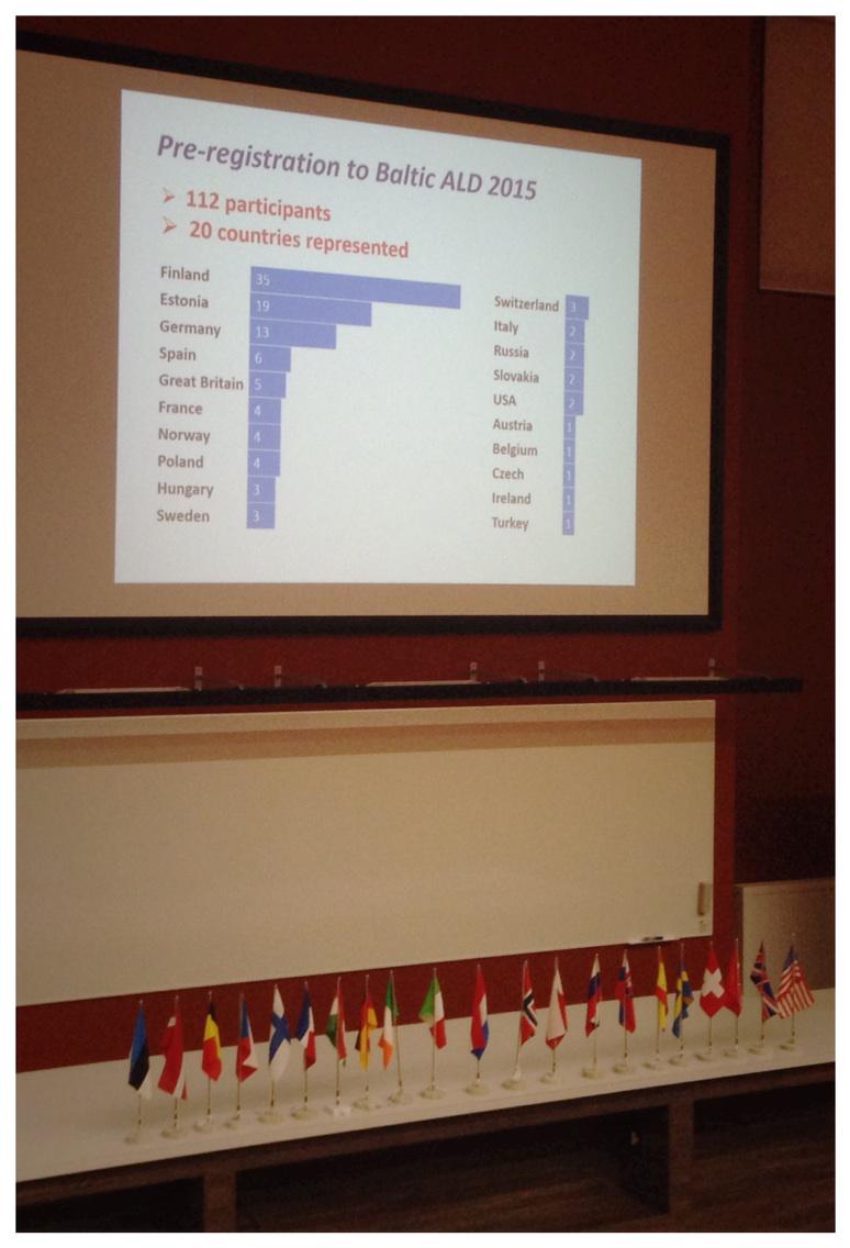
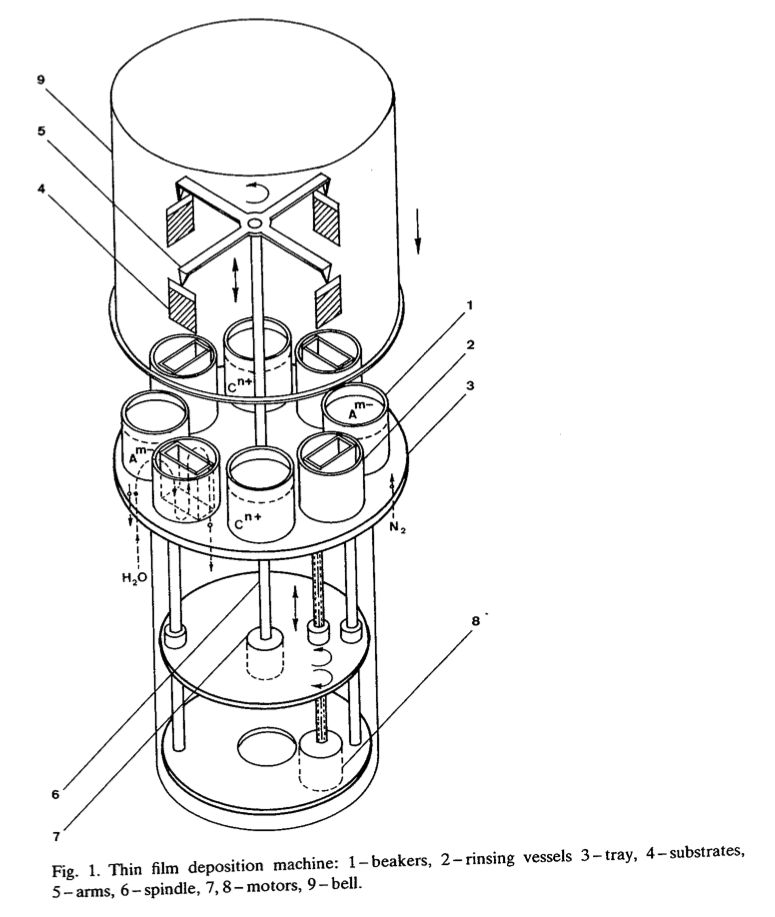
Saturday, October 3, 2015

Graphene as a front contact for silicon-perovskite tandem solar cells

As reported by HZB : HZB team develops elegant process for coating fragile perovskite layers with graphene for the first time. Subsequent measurements show that the graphene layer is an ideal front contact in several respects.

The perovskite film (black, 200-300 nm) is covered by Spiro.OMeTAD, Graphene with gold contact at one edge, a glass substrate and an amorphous/crystalline silicon solar cell. Credit: F. Lang / HZB

Silicon absorbers primarily convert the red portion of the solar spectrum very effectively into electrical energy, whereas the blue portions are partially lost as heat. To reduce this loss, the silicon cell can be combined with an additional solar cell that primarily converts the blue portions. Teams at HZB have already acquired extensive experience with these kinds of tandem cells. A particularly effective complement to conventional silicon is the hybrid material called perovskite. It has a band gap of 1.6 electron volts with organic as well as inorganic components. However, it is very difficult to provide the perovskite layer with a transparent front contact. While sputter deposition of indium tin oxide (ITO) is common practice for inorganic silicon solar cells, this technique destroys the organic components of a perovskite cell.
 

Graphene as transparent front contact:

Now a group headed by Prof. Norbert Nickel has introduced a new solution. Dr. Marc Gluba and PhD student Felix Lang have developed a process to cover the perovskite layer evenly with graphene. Graphene consists of carbon atoms that have arranged themselves into a two-dimensional honeycomb lattice forming an extremely thin film that is highly conductive and highly transparent.

Fishing for graphene:

As a first step, the scientists promote growth of the graphene onto copper foil from a methane atmosphere at about 1000 degrees Celsius. For the subsequent steps, they stabilise the fragile layer with a polymer that protects the graphene from cracking. In the following step, Felix Lang etches away the copper foil. This enables him to transfer the protected graphene film onto the perovskite. “This is normally carried out in water. The graphene film floats on the surface and is fished out by the solar cell, so to speak. However, in this case this technique does not work, because the performance of the perovskite degrades with moisture. Therefore we had to find another liquid that does not attack perovskite, yet is as similar to water as possible”, explains Gluba.

Ideal front contact:

Subsequent measurements showed that the graphene layer is an ideal front contact in several respects. Thanks to its high transparency, none of the sunlight’s energy is lost in this layer. But the main advantage is that there are no open-circuit voltage losses, that are commonly observed for sputtered ITO layers. This increases the overall conversion efficiency. “This solution is comparatively simple and inexpensive to implement”, says Nickel. “For the first time, we have succeeded in implementing graphene in a perovskite solar cell. This enabled us to build a high-efficiency tandem device.”
 

Perovskite Solar Cells with Large-Area CVD-Graphene for Tandem Solar Cells

Felix Lang, Marc A. Gluba, Steve Albrecht, Jörg Rappich, Lars Korte, Bernd Rech, and Norbert H. Nickel
J. Phys. Chem. Lett., 2015, 6 (14), pp 2745–2750
DOI: 10.1021/acs.jpclett.5b0117

Thursday, October 1, 2015

Photoshow Baltic ALD 2015 in Tartu Estonia

Here pictures in social media and that you send to me (jonas.sundqvist@baldengineering.com) will be publish to cover the scientific and social program of The 13th International Baltic Conference on Atomic Layer Deposition will be held in Tartu, Estonia, at the Institute of Physics of the University of Tartu on September 28–29, 2015.

Twitter Hash Tag : #BalticALD


Following the Baltic ALD 2015 Conference, the annual meeting of the COST project HERALD 
(http://www.european-ald.net) will be held at Dorpat Conference Center, Tartu, on September 30, 2015. Please also take picture at this event!


SCIENTIFIC PROGRAM:

http://bald2015.ee/program-baltic-ald-2015/schedule/

 Book of abstracts (Riikka Puurunen, VTT, Twitter)

A bus load of ALD scientists from Helsinki heading for the Helsinki-Tartu flight. Last time (2002) they took the bus all the way to Tartu.

Tartu as viewed from the conference Hotel on Sunday afternoon (Irina Kärkkänen, Sentech)

Conference bag - must be the best looking bag ever in the History of ALD (Riikka Puurunen, VTT, Twitter)

 The Russian ALD bag next to the Estonian ALD Bag below the VPHA Poster (Riikka Puurunen, VTT, Twitter)

 Participant distribution - Finland on top followed by Estonia and Germany (Riikka Puuronen, VTT, Twitter)

 View at the podium (Simon Rushworth, EpiValance, LinkedIn)

Modeling area-selective ALD, talk by Simon Elliott Tyndall (Riikka Puurunen, Twitter)

Timo Vähä-Ojala from Picosun talked about modelling of gas flow in ALD reactor (Tero Pilvi, Picosun)

Riikka Puurunen VTT -  Mechanical property mapping of ALD thin films (Christoph Hossbach, TU-Dresden) 

SOCIAL PROGRAM:

"Colours, colours! Physicum building at Tartu University" (Riikka Puurunen,  VTT, Twitter)


Welcome Reception September 27, 2015
Conference Dinner September 28, 2015

"Conference dinner at AHHAA science centre was memorable with the pyro show, good food, music, and company" (Riikka Puurunen, VTT, Twitter)

Guided City Tours September, 29, 2015 

SPONSORING


The conference venue showing the Exhibition area for a number of sponsoring companies: Armgate, Picosun, Oxford Instruments, Beneq, STREM Chemicals, SENTECH Instruments, Semilab, FAB Support.


Atomic Layer Deposition from Dissolved Precursors

Funny, I was just discussing an early french publication (see below) )from 1984 on Twitter with Riikka Puurunen with respect to the VPHA project and almost instantly I got an e-mail alert on this very cool publication in Nano Letter from Julien Bachmann and Lionel Santinacci (Hello again!) and co-workers on the same topic (liquid ALD) - hmm no early night tonight either... 

Atomic Layer Deposition from Dissolved Precursors

Yanlin Wu, Dirk Döhler, Maïssa Barr, Elina Oks, Marc Wolf, Lionel Santinacci, and Julien Bachmann

Department of Chemistry and Pharmacy, Friedrich-Alexander University of Erlangen-Nürnberg, Egerlandstrasse 1, D−91058 Erlangen, Germany
¥ CNRS, CINaM UMR 7325, Aix Marseille Université, F−13288 Marseille, France
‡ Departments of Chemistry and Physics, University of Hamburg, Sedanstrasse 19, D−20146 Hamburg, Germany
Nano Lett., Article ASAP
DOI: 10.1021/acs.nanolett.5b01424


Abstract

We establish a novel thin film deposition technique by transferring the principles of atomic layer deposition (ALD) known with gaseous precursors toward precursors dissolved in a liquid. An established ALD reaction behaves similarly when performed from solutions. “Solution ALD” (sALD) can coat deep pores in a conformal manner. sALD offers novel opportunities by overcoming the need for volatile and thermally robust precursors. We establish a MgO sALD procedure based on the hydrolysis of a Grignard reagent.


An amazing Spatial Liquid ALD machine from the mid 1980s (Nicolau1985, CEA, FRA) 


Wednesday, September 30, 2015

The fundamentals of CVD of boron-carbon thin films


Here is a great publication on the fundamentals of CVD of boron-carbon thin films from Henrik Pedersen and co-wokers at Linköping University, Sweden and Philipps-Universität Marburg. Such freedom they have, with respect to temperature... but then again it is rather cold in Sweden.

Gas phase chemical vapor deposition chemistry of triethylboron probed by boron–carbon thin film deposition and quantum chemical calculations

Mewlude Imam, Konstantin Gaul, Andreas Stegmüller, Carina Höglund, Jens Jensen, Lars Hultman, Jens Birch, Ralf Tonner and Henrik Pedersen

J. Mater. Chem. C, 2015, Advance Article
DOI: 10.1039/C5TC02293B

We present triethylboron (TEB) as a single-source precursor for chemical vapor deposition (CVD) of BxC thin films and study its gas phase chemistry under CVD conditions by quantum chemical calculations. A comprehensive thermochemical catalogue for the species of the gas phase chemistry of TEB is examined and found to be dominated by β-hydride eliminations of C2H4 to yield BH3. A complementary bimolecular reaction path based on H2 assisted C2H6 elimination to BH3 is also significant at lower temperatures in the presence of hydrogen. Furthermore, we find a temperature window of 600–1000 °C for the deposition of X-ray amorphous BxC films with 2.5 ≤ x ≤ 4.5 from TEB. Films grown at temperatures below 600 °C contain high amounts of H, while temperatures above 1000 °C result in C-rich films. The film density and hardness are determined to be in the range of 2.40–2.65 g cm−3 and 29–39 GPa, respectively, within the determined temperature window.

Ruthenium may take over from Copper for advanced Interconencts according to Imec

Here is an interesting report by Jeff Dorsch from SEMI’s annual Strategic Materials Conference, that was held September 22-23, at the Computer History Museum in Mountain View, California.

One of the most interesting things i find i that ruthenium is back on the table, at least according to Imecs Christoph Adelmann who presented that ruthenium my take over from copper in advanced interconnects one day. This is not the first time ruthenium is announced entering into semiconductor manufacturing. Many ruthenium R&D programs has started and eneded many times the last decade at IDMs, OEMs and materials suppliers especially at DRAM manufacturers looking to integrate SrTiO3 super high-k using ruthenium based electrodes in the capacitor module. So it is time again to have a look at the Ruthenium price development at Johnson Matthey.

Today the ruthenium price is actually as low (~150$/Oz.) as is was the first time I got involved in ruthenium ALD/CVD development in 2003 at Infineon. It will be very interesting to follow ruthenium this time  and if it would actually enter BEOL metallization the price should go up considerably since it does come again many times an an advance interconnect chip 12-16 depending on the design but not all layers may have to contain ruthenium so the upper layer will stay copper for a long time to come. Anotehr driver for sure is if ruthenium were to be used in 3D-stacing TSV technology - Maybe a good timing now to invest in some ruthenium!


Pt & Ru price chart generated at http://www.platinum.matthey.com/prices


Platinum, RutheniumMonthly Average prices between 30 Sep 2000 and 30 Sep 2015JM Base Price $/0zPlatinum average: $1,165.38, Ruthenium average: $150.59 - See more at: http://www.platinum.matthey.com/prices/price-charts#sthash.GMP3wwcI.dpuf


Platinum, RutheniumMonthly Average prices between 30 Sep 2000 and 30 Sep 2015JM Base Price $/0zPlatinum average: $1,165.38, Ruthenium average: $150.59 - See more at: http://www.platinum.matthey.com/prices/price-charts#sthash.GMP3wwcI.dpuf

The agenda for the ALD Lab Dresden Symposium at SEMICON Europa is now set!

The agenda for the ALD Lab Dresden Symposium is now set! If you are attending and representing a company or any organization with an offering in ALD or ALE - please brig alog your flyers, coffee mugs, hats and pensand I will sort out a table that is bug enought for displaying it.


AGENDA


 Tuesday, 6 October 2015

 09:00WelcomeOrganized by:


Supported by:

cost logo


Prof. Johann W. Bartha, TU Dresden

 09:15In situ monitoring of Atomic Layer Deposition in porous materials

Martin Knaut, TU Dresden

 09:40Passivation of MEMS by Atomic Layer Deposition

Matthias Schwille, Robert Bosch

 10:05Growth Monitoring by XPS and LEIS Investigations of Ultrathin Copper Films Deposited by Atomic Layer Deposition

Dileep Dhakal, TU Chemnitz/FhG ENAS

 10:30High-k dielectrics by ALD for BEOL compatible MIM

Wenke Weinreich, FhG IPMS-CNT


 10:55ALD coatings for applications as permeation barrier and protective layer in fiber-reinforced materials
Mario Krug, FhG IKTS


 11:20ALD for solar cell application
Ingo Dirnstorfer, NaMLab


 11:45Plasma enhanced ALD process for TiO2- and WO3- films

Alexander Strobel, FH Zwickau


 12:10Lunch Break (Conversation, Networking, Finger food)


 13:00Why do we need Atomic Layer Etching

Jonas Sundqvist, Lund University/TU Dresden


 13:25Spatial Atomic Layer Deposition and Atomic Layer Etching

Prof. Fred Roozeboom, TU Eindhoven/ TNO Eindhoven


 13:50Atomic Layer Etching: What Can We Learn from Atomic Layer Deposition?

Harm Knoops, Oxford Instruments/TU Eindhoven


 14:15Hardmask and side wall protection during dry etching with plasma enhanced deposition during dry etching for ALE purposes

Stephan Wege, Plasway


 14:40Industrial High Throughput Atomic Layer Deposition Equipment and Process for OLED Encapsulation

Jacques Kools, Encapsulix


 15:05Closing Remarks / Wrap Up

Prof. Johann W. Bartha, TU Dresden


 15:10End

Tuesday, September 29, 2015

ALD at The 228th ECS Meeting October 11-15, 2015 in Phoenix AZ

Here are some interesting sessions at the upcoming The 228th ECS Meeting October 11-15, 2015 in Phoenix Arizona. Looking forward to hear about the outcome of the panel discussion on ALE!


G01 Atomic Layer Deposition Applications 11

Lead Organizer: F. Roozeboom (Eindhoven University of Technology)
Co-organizers: Jeffrey W Elam (Argonne National Laboratory) , A. Londergan (Qualcomm Technologies, Inc.) , O. van der Straten (IBM Research) , Annelies Delabie (imec) and Stefan De Gendt (imec vzw)

Tuesday, October 13, 2015

08:30-10:00

Energy Applications I
Phoenix East
Chair(s): Jeffrey W Elam and Fred Roozeboom

10:00-12:20

Energy Applications II
Phoenix East
Chair(s): Jeffrey W Elam and Neil P. Dasgupta

14:00-16:40

Textile and Related Coatings
Phoenix East
Chair(s): J. W. Elam and Helmut Baumgart

16:40-17:20

Characterization
Phoenix East
Chair(s): Stefan De Gendt and Jesse S Jur

Wednesday, October 14, 2015

09:00-10:00

New Materials and Processes I
Phoenix East
Chair(s): Stefan De Gendt and Paul Raymond Chalker

10:00-12:20

New Materials and Processes II
Phoenix East
Chair(s): O. van der Straten and Stefan De Gendt

14:00-15:40

Metal Deposition and Applications I
Phoenix East
Chair(s): O. van der Straten and Sean Barry

15:40-16:40

Metal Deposition and Applications II
Phoenix East
Chair(s): O. van der Straten and Soo-Hyun Kim

18:00-20:00

G01 Poster Session
West Hall 1
Chair(s): Fred Roozeboom

Thursday, October 15, 2015

08:00-10:00

Atomic Layer Etching I
Phoenix East
Chair(s): Fred Roozeboom and Thorsten Lill

10:00-11:40

Atomic Layer Etching II
Phoenix East
Chair(s): Craig Huffman and Steven M. George

11:40-12:40

Panel Discussion on Atomic Layer Etching
Phoenix East
Chair(s): Craig Huffman

Monday, September 28, 2015

Gerogia Tech have demonstrated the first optical rectenna using CNTs and ALD

Using nanometer-scale components - carbon nanotubes and atomic layer deposition researchers at Gerogia Tech have demonstrated the first optical rectenna, a device that combines the functions of antennas and a rectifier diodes to convert light directly into DC current. This could be a future technology to make very efficient solar cells!


Georgia Tech associate professor Baratunde Cola measures the power produced by converting green laser illumination to electricity using the carbon nanotube optical rectenna. (Phys.org)


Youtube interview of Prof. Cola

Read more at: http://phys.org/news/2015-09-optical-rectennacombined-rectifier-antennaconverts-dc.html#jCp

Origin and History of Electro Luminescent Displays

As many of you know, Dr. Tuomo Suntola and co-workes invented many ALD technologies and processes and further developed Atomic Layer Deposition (ALD), then called Atomic Layer Epitaxy (ALE) to an industrial mass production process during the 70s and 80s. They did this in order to have a reliable manufacturing method with atomic level control of dopants and crystallinity of the individual thin film layers making up the EL device for producing Electro Luminescent Displays with reliable operation. Most ALD experts has com across this story numerous times and that is why it is interesting to read about it from a wider perspective. Here is an excellent article on the origin and history of EL Displays worth reading also including the early 20th century discoveries and work on electroluminescense and other big players like SHARP.

http://www.elwire.net/products/electroluminescent-displays/


For more ALD related information and History of they development that took place in Finland you should also visit the ADL 2014 Kyoto Tutorial by Riikka Puuronen (VTT, Finland) which is available at Slideshare: http://www.slideshare.net/RiikkaPuurunen/aldhistory-tutorial-in-kyoyo-al-dhistory-tutorialald2014riikkapuurunen20140615 (Slide above, Riikka Puurunen, VTT))

If you´re interest in more early history of ALD you should read about or join the VHPA Project - it is quite exciting!

Virtual Project on the History of ALD (VPHA)

VPHA is an open collaborative effort, whose goal is to clarify open questions related to the early history of the Atomic Layer Deposition (ALD) thin film deposition technique. VPHA was launched in July 2013. VPHA is based on voluntary efforts, and anyone interested in the history of ALD is welcome to join. All VPHA activities are made in an atmosphere of openness, respect and trust.

http://www.vph-ald.com

Sunday, September 27, 2015

UPDATE- Photo show from Baltic ALD 2015 September 28-29, Tartu, Estonia

Here pictures in social media and that you send to me (jonas.sundqvist@baldengineering.com) will be publish to cover the scientific and social program of The 13th International Baltic Conference on Atomic Layer Deposition will be held in Tartu, Estonia, at the Institute of Physics of the University of Tartu on September 28–29, 2015.

Twitter Hash Tag : #BalticALD


Following the Baltic ALD 2015 Conference, the annual meeting of the COST project HERALD 
(http://www.european-ald.net) will be held at Dorpat Conference Center, Tartu, on September 30, 2015. Please also take picture at this event!


SCIENTIFIC PROGRAM:

http://bald2015.ee/program-baltic-ald-2015/schedule/

 Book of abstracts (Riikka Puurunen, VTT, Twitter)

A bus load of ALD scientists from Helsinki heading for the Helsinki-Tartu flight. Last time (2002) they took the bus all the way to Tartu.

Tartu as viewed from the conference Hotel on Sunday afternoon (Irina Kärkkänen, Sentech)

Conference bag - must be the best looking bag ever in the History of ALD (Riikka Puurunen, VTT, Twitter)

 The Russian ALD bag next to the Estonian ALD Bag below the VPHA Poster (Riikka Puurunen, VTT, Twitter)

 Participant distribution - Finland on top followed by Estonia and Germany (Riikka Puuronen, VTT, Twitter)

 View at the podium (Simon Rushworth, EpiValance, LinkedIn)

Modeling area-selective ALD, talk by Simon Elliott Tyndall (Riikka Puurunen, Twitter)

Timo Vähä-Ojala from Picosun talked about modelling of gas flow in ALD reactor (Tero Pilvi, Picosun)

Riikka Puurunen VTT -  Mechanical property mapping of ALD thin films (Christoph Hossbach, TU-Dresden) 

SOCIAL PROGRAM:

"Colours, colours! Physicum building at Tartu University" (Riikka Puurunen,  VTT, Twitter)


Welcome Reception September 27, 2015
Conference Dinner September 28, 2015

"Conference dinner at AHHAA science centre was memorable with the pyro show, good food, music, and company" (Riikka Puurunen, VTT, Twitter)

Guided City Tours September, 29, 2015 

SPONSORING


The conference venue showing the Exhibition area for a number of sponsoring companies: Armgate, Picosun, Oxford Instruments, Beneq, STREM Chemicals, SENTECH Instruments, Semilab, FAB Support.


Friday, September 25, 2015

Zinc based transistor demonstrated by Korea University and Samsung


As reported by American Institute of Physics - Researchers set speed records for zinc-based transistors with argon plasma process


Researchers set speed records for zinc-based transistors with argon plasma process 


A cross-sectional high angle annular dark field scanning transmission electron microscopy (HAADF-STEM) image and nanobeam diffraction pattern of Ar plasma treated ZnON. Credit: E. Lee & S. Jeon/Samsung Advanced Institute of Technology & Korea University

Researchers at Korea University and the Samsung Advanced Institute of Technology have now developed a new type of thin film transistor that's significantly faster than its predecessors—an important step toward speeding up image display on devices like TVs and smartphone screens. The scientists made the transistor from zinc oxynitride, or ZnON, which they then plasma treated with argon gas.

More information: "Ar plasma treated ZnON transistor for future thin film electronics," by Eunha Lee, Teaho Kim, Anass Benayad, HeeGoo Kim, Sanghun Jeon and Gyeong-Sy Park, Applied Physics Letters on September 22, 2015. DOI: 10.1063/1.4930827

Powder Coating Industries Choose Picosun's ALD Solutions

Picosun Oy, leading supplier of Atomic Layer Deposition (ALD) thin film coating solutions for industrial manufacturing, reports delivery of multiple powder coating ALD systems to key production customers.


Picosun offers powder coating solutions for both industry and R&D. Our POCA™ 300 powder coating cartridge allows processing of large batches of materials and it can be directly integrated into the PICOSUN™ P-300 production-scale reactor frame. For smaller material volumes, our POCA™ 200 powder coating cartridge integrated into a PICOSUN™ R-series tool is a compact, versatile, and cost-efficient solution for top quality powder materials research. Picosun’s novel, innovative PICOVIBE™ feature improves the powder coating process even further by enhancing the distribution of the precursor vapors inside the powder batch, resulting in uniform film formation on every particle.
 
Surface modification of powder materials is a central requirement in various industry segments. Catalysts, novel battery materials, light-emitting phosphors, and medical substances are prime examples where Picosun's ALD technology enables completely new products or creates unparalleled added value to existing ones. Picosun's patented, highly successful POCA™ powder coating product family covers both research and pilot production tools and systems optimized for large scale batch manufacturing, all designed solely based on the requirements of the ALD method. All POCA™ systems can be equipped with Picosun's innovative Picovibe™ mechanism for optimal formation of highest quality ALD film throughout the batch.

"Staying constantly on the top of current and coming industrial trends is one of the cornerstones of Picosun's success. Functionalization of powder materials with ALD is one of our key application areas, and the market is huge. We are happy to see that the investment we have placed in development and optimization of our powder processing solutions now pays itself back in the form of repeat sales of our powder coating tools to our key industry customers, realizing their most advanced products in e.g. lighting device and medical industries," states Juhana Kostamo, Managing Director of Picosun.

Low temperature PEALD of SiN moisture permeation barrier layers from TU Eindhoven

This is really interesting! SiN is the fastest growing ALD film application in leading edge CMOS - for CVD it is I guess the opposite trend ;-) (originally posted by ALDPulse.com)

Low temperature plasma-assisted atomic layer deposition of silicon nitride moisture permeation barrier layers

Anne-Marije Andringa, Alberto Perrotta, Koen de Peuter, Harm C.M. Knoops, Wilhelmus M.M Kessels, and Mariadriana Creatore
ACS Appl. Mater. Interfaces, Just Accepted Manuscript
DOI: 10.1021/acsami.5b06801
Publication Date (Web): September 22, 2015


Encapsulation of organic (opto-)electronic devices, such as organic light-emitting diodes (OLEDs), photovoltaic cells and field-effect transistors, is required to minimize device degradation induced by moisture and oxygen ingress. SiNx moisture permeation barriers have been fabricated using a very recently developed low temperature plasma-assisted atomic layer deposition (ALD), consisting of half-reactions of the substrate with the precursor SiH2(NHtBu)2 and with a N2-fed plasma. The deposited films have been characterized in terms of refractive index and chemical composition by spectroscopic ellipsometry (SE), X-ray photoelectron spectroscopy (XPS) and Fourier-transform infrared spectroscopy (FTIR), respectively. The SiNx thin film refractive index ranges from 1.80 to 1.90 for films deposited at 80 °C up to 200 °C, respectively, and the C, O and H impurity levels decrease when increasing the deposition temperature. The relative open porosity content of the layers has been studied by means of multi-solvent ellipsometric porosimetry (EP), adopting three solvents with different kinetic diameter: water (~ 0.3 nm), ethanol (~ 0.4 nm) and toluene (~ 0.6 nm). Irrespective of deposition temperature and hence impurity content in the SiNx films, no uptake of any adsorptive has been observed, pointing out the absence of open pores larger than 0.3 nm in diameter. Instead, multilayer development has been observed, leading to type II isotherms which, according to the IUPAC classification, are characteristic of non-porous layers. The calcium test has been performed in a climate chamber at 20 °C and 50% relative humidity to determine the intrinsic water vapor transmission rate (WVTR) of SiNx barriers deposited at 120 °C. Intrinsic WVTR values in the range of 10-6 g/m2/day indicate excellent barrier properties for ALD SiNx layers as thin as 10 nm, competing with the state-of-the-art plasma-enhanced chemical vapor deposited SiNx layers of a few hundreds nanometers- thick.