Sunday, October 11, 2015

UK collaboration seeks to develop new ultra-barrier materials based on graphene interlayers & roll to roll ALD

As reported by New Electronics : The Centre of Process Innovation (CPI) has announced that it has joined a UK based collaboration called ‘Gravia’, to develop the next generation of ultra-barrier materials using graphene for the production of flexible transparent plastic electronic based displays for the next generation of smartphones, tablets and wearable electronics.


The graphene market is predicted to be worth more than £800million by 2023 and could transform the manufacturing landscape in the UK.The project, including the University of Cambridge, FlexEnable and the National Physical Laboratory (NPL), expects to deliver a feasible material and process system. It builds upon existing investments by Innovate UK and the EPSRC in this area.


CPI Cleanroom

“The collaboration brings together world class supply chain expertise across the UK to bridge the gap from Graphene research to the manufacturing of commercial flexible display screens,” said James Johnstone, business development manager at CPI. 

“CPI’s role in the project is to use roll-to-roll atomic layer deposition technologies to scale up, test and fabricate the ultra barrier materials.”


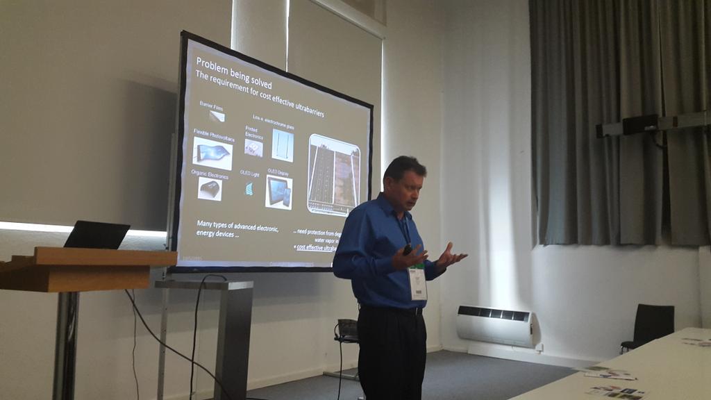
Beneq Roll to Roll Atomic Layer Deposition Tool - CPI offers a roll to roll atomic layer deposition (ALD) tool which is capable of handling films up to 600mm wide with thicknesses ranging from 20 – 200 µm and can produce an active coat width of 480mm.

The incorporation of graphene interlayers offers potential for flexible displays. Its gas blocking properties will enable barrier materials that are flexible, transparent, robust, and impervious to many molecules. Gravia will seek to accelerate product development, improving upon current ultra barrier performance and lifetimes by producing consistent barrier materials and processes on large area substrates by utilising specialist growth techniques. The key challenge will be to develop large-area poly-crystalline graphene films which maximise performance whilst mitigating process imperfections.

TEL signs $262 million deal with SUNY Poly to stay in Albany

As reported by Times Union : Tokyo Electron Ltd. has signed a five-year, $262.5 million extension of its research and development agreement with SUNY Polytechnic Institute in a deal that keeps the Japanese computer chip manufacturing equipment maker in Albany through 2020.


The agreement, which took effect Oct. 1 and will be officially announced Thursday, comes 12 years after the company, known in the industry as TEL, chose Albany for its first research lab outside of Japan.


The newly inked deal also is critical because TEL, which makes manufacturing equipment used in chip factories, or "fabs," is expected to play a key role in one or more manufacturing development programs in Albany involving at least $1 billion in spending by the semiconductor industry and hundreds of new jobs, the exact details of which have yet to be made public.


"New York continues to be a wonderful partner to TEL," Tetsuro Higashi, CEO of TEL said in a statement provided to the Times Union. "Through SUNY Poly, Gov. Cuomo has created one of the finest R&D centers in the world for creating next-generation chip technology, and we look forward to our continued collaboration and innovation."

Wednesday, October 7, 2015

3M licensing agreement with Lotus Applied Technology TransFlexALDTM spatial ALD

As reported today : 3M has entered into a licensing agreement with Lotus Applied Technology to access Lotus’s TransFlexALDTM spatial Atomic Layer Deposition (ALD) and barrier materials patent portfolio. TransFlexALD technology enables high-speed, low-cost deposition of single layer “ultra-barrier” coatings on rolls of polymer film using ALD. These coatings play a critical role in the encapsulation of moisture- and oxygen-sensitive electronics, such as OLED (organic light emitting device) lighting and displays, quantum dot films, photovoltaics, and flexible electronics.


“We are pleased to partner with Lotus AT and for the potential of their ALD technology to expand our ultra barrier film solutions portfolio as we integrate it with 3M’s proven technology strengths,” said John Banovetz, vice president of 3M’s Corporate Research Laboratory. “This licensing agreement and our continued product innovation will help 3M increase the performance of our ultra barrier films and offer cost-effective barrier solutions that will allow our customers to provide more competitive products in the flexible electronics markets they serve.”

3M is a leading manufacturer of flexible, transparent ultra barrier films providing encapsulation solutions for display (3M™ Flexible Transparent Barrier Film) and other sensitive electronic applications.


“We are excited to partner with 3M, a distinguished technology leader in the field of ultra barrier films,” said Eric Dickey, president of Lotus Applied Technology. “This technology offers the opportunity to radically improve the performance of single-layer barrier coatings, and 3M’s experience and expertise in this field will enable its rapid deployment in a field of applications that have been demanding higher performance at lower cost.”


(http://lotusat.com) Founded in 2007, Lotus Applied Technology was formed through a spinoff of the thin film process group within Planar Systems, Inc., a pioneer in Atomic Layer Deposition technology and manufacturing. Housed in a fully dedicated 20,000 square foot thin film processing and R&D facility in Hillsboro, Oregon, our team of technologists has been working together for over 20 years, developing innovative solutions to thin film processing challenges. Our equipment set includes a wide array of thin film deposition, lithography, and patterning equipment, including a versatile set of ALD equipment:

  • Six P400 Conventional Pulse-Based Batch ALD reactors
  • Roll to Roll ALD Research Scale Reactor
  • TransFlex Roll to Roll ALD Pilot Scale Reactor
  • Vortex Rotary Batch Reactor

Atomic Layer Processing at SEMICON Europa 2015

Here are some ALD related pictures from SEMICON Europa in Dresden. Not only ALD since this year ALE and RIE was also a hot topic in the afternoon of the ALD Lab Dresden Symposium on Tuesday (see previous post). Biggest news here is that Oxford Instruments has released new innovative hardware for ALE!


Oxford Instruments releasing new innovative hardware for ALE (Atomic Layer Etching). Harm Knoops (right) and Andreas Stamm (left)


Assuming Oxford Instrument have big success with selling ALE hardware we will definitely start seeing an increase in ALE publications in the future and maybe the upward trend of ALD will follow or the technologies will merge into one for "Atomic Layer Processing" or like some of  us like to call it - ALX. This was actually the message from many of the presenter in the ALD Symposium (Prof. Bartha, Prof. Roozeboom, and Stephan Wege from Plasway), including this one from myself. The OEM market for ALX will definitely be very innovative and interesting in the years to come.


The Sentech stand a German OEM selling both Etch, PECVD and ALD / PEALD equipment together with very powerful in-situ ellipsometry metrology.


Nice to see that there is a lot of new activities in the European precursor supplier business. Here the team from EpiValence. EpiValence is focusing on working in collaboration with organisations looking for advanced chemicals and materials. Starting with research and development through to full scale up. You may also notice the close collaboration with iCAM (see their stand futher below)


A cross section of the popular Japanese ALD valves from KTZ SCT


Plasma Therm makes very technological advanced ICP RIE tools (Versaline) with lamp heated (!) chambers. Why these guys don´t make a PEALD chamber I don´t know - fast gas switching they do master for their Plasma wafer dicing process, which seems to be their cash cow.


Quick stop at the STREM  to talk to Jamal Belgacem about some need for new precursor and to pick up the latest catalogues for ALD precursors


I had a nice chat with Peter Barlow at iCAM - The Bubbler Maters from Wales - about building a new flexible solid evaporator for precursor screening. 


Tuesday, October 6, 2015

Photoshow : ALD Lab Dresden Symposium at SEMICON Europa 2015

SEMICON Europa this year has turned out to be a major event for ALD and exciting nanoelectronic materials research. Here are photos taken from The ALD Day October 6th, 2015!

More details on this event you can find here : http://baldengineering.blogspot.de/2015/10/ald-ale-and-exciting-nanoelectronic.html

We are already looking forward to SEMICON Europa 2016 in Grenoble, France and to co-chair an ALD Sympoium there yet one more time!

SEMICON Europa ALD 2014, Grenoble : http://baldengineering.blogspot.de/2014/10/voila-3rd-ald-lab-dresden-symposium-at.html


Columbus, Tuesday Oct 6, 13:45, ALD / ALE Sympoium of The ALD Lab Dresden, Messe Dreaden, Germany


Waiting for the ALD Storm!


Welcome
Prof. Johann W. Bartha, TU Dresden


In situ monitoring of Atomic Layer Deposition in porous materials
Martin Knaut, TU Dresden


Passivation of MEMS by Atomic Layer Deposition
Matthias Schwille, Robert Bosch


Symposium is full - please help me throw out a PVD guy


Growth Monitoring by XPS and LEIS Investigations of Ultrathin Copper Films Deposited by Atomic Layer Deposition
Dileep Dhakal, TU Chemnitz/FhG ENAS


High-k dielectrics by ALD for BEOL compatible MIM
Wenke Weinreich, FhG IPMS-CNT


ALD coatings for applications as permeation barrier and protective layer in fiber-reinforced materials
Mario Krug, FhG IKTS


ALD for solar cell application
Ingo Dirnstorfer, NaMLab


Plasma enhanced ALD process for TiO2- and WO3- films
Alexander Strobel, FH Zwickau


Why do we need Atomic Layer Etching
Jonas Sundqvist, Lund University/TU Dresden


Spatial Atomic Layer Deposition and Atomic Layer Etching
Prof. Fred Roozeboom, TU Eindhoven / TNO Eindhoven


Atomic Layer Etching: What Can We Learn from Atomic Layer Deposition?
Harm Knoops, Oxford Instruments/TU Eindhoven


Hardmask and side wall protection during dry etching with plasma enhanced deposition during dry etching for ALE purposes
Stephan Wege, Plasway


Industrial High Throughput Atomic Layer Deposition Equipment and Process for OLED Encapsulation
Jacques Kools, Encapsulix


Monolayer controlled deposition of 2D transition metal dichalcogenides on large area substrates
Annelies Delabie, Imec


Selective Deposition as Enabler for Shrinking Device Dimensions

Suvi Haukka, Executive Scientist, ASM Microchemistry Ltd.


Saturday, October 3, 2015

TECHCET -Dielectric Precursors – NEW – Just Released!

The Dielectric Precursors Report provide detailed market, supply chain and technology trend information required for anyone developing strategy for their business, be it a materials supplier or semiconductor chip manufacturer. Precursor types include, gapfill, ILD, low K, and multi-patterning.


Click here for full table of contents:


Workshop Simulation of chemistry-driven growth phenomena for metastable materials

CECAM/Psi-k/HERALD Workshop
Simulation of chemistry-driven growth phenomena for metastable materials


The controlled growth of thin films based on metastable materials by chemistry-driven processes is of high technological importance for topics like semiconductor devices or optical coatings. Computational modelling of this inherently multiscale process is crucial for an atomistic understanding and enables a decoupling and separate optimization of the growth-determining factors of non-equilibrium materials. This workshop will result in a joint effort by experts from different modelling communities covering the necessary length and time scales.
The workshop will be held at

nearby Marburg in Germany from November 08-11, 2015.
 

Organizers

CECAM Psi-k HERALD
   

Sponsors

GRK 1782 ESFDock/Chemicals
 

ALD, ALE and exciting nanoelectronic materials research at SEMICON Europa, 6-8 October, Dresden

SEMICON Europa this year has turned out to be a major event for ALD and exciting nanoelectronic materials research. Here are I have have highlighted some of the events with respect to this.


Columbus, Tuesday Oct 6, 13:45, ALD / ALE Sympoium of The ALD Lab Dresden

09:00WelcomeOrganized by:


Supported by:

cost logo


Prof. Johann W. Bartha, TU Dresden

 09:15In situ monitoring of Atomic Layer Deposition in porous materials

Martin Knaut, TU Dresden

 09:40Passivation of MEMS by Atomic Layer Deposition

Matthias Schwille, Robert Bosch

 10:05Growth Monitoring by XPS and LEIS Investigations of Ultrathin Copper Films Deposited by Atomic Layer Deposition

Dileep Dhakal, TU Chemnitz/FhG ENAS

 10:30High-k dielectrics by ALD for BEOL compatible MIM

Wenke Weinreich, FhG IPMS-CNT


 10:55ALD coatings for applications as permeation barrier and protective layer in fiber-reinforced materials
Mario Krug, FhG IKTS


 11:20ALD for solar cell application
Ingo Dirnstorfer, NaMLab


 11:45Plasma enhanced ALD process for TiO2- and WO3- films

Alexander Strobel, FH Zwickau


 12:10Lunch Break (Conversation, Networking, Finger food)


 13:00Why do we need Atomic Layer Etching

Jonas Sundqvist, Lund University/TU Dresden


 13:25Spatial Atomic Layer Deposition and Atomic Layer Etching

Prof. Fred Roozeboom, TU Eindhoven / TNO Eindhoven


 13:50Atomic Layer Etching: What Can We Learn from Atomic Layer Deposition?

Harm Knoops, Oxford Instruments/TU Eindhoven


 14:15Hardmask and side wall protection during dry etching with plasma enhanced deposition during dry etching for ALE purposes

Stephan Wege, Plasway


 14:40Industrial High Throughput Atomic Layer Deposition Equipment and Process for OLED Encapsulation

Jacques Kools, Encapsulix


 15:05Closing Remarks / Wrap Up

Prof. Johann W. Bartha, TU Dresden


 15:10End

TECH ARENA, Tuesday Oct 6, 13:45- Emerging Research, Materials and Processes Session

Potential Solutions to Semiconductor Industry’s Challenges


Chair Hessel Sprey, Manager cooperative programs and university contacts, ASM International
13:45 Introduction
13:50
Next Generation Ferroelectric Field Effect Transistors enabled by Ferroelectric Hafnium Oxide
Thomas Mikolajick, scientific director, NaMLab Gmbh / TU Dresden
14:15
Large diameter GaN-on-Si epiwafers for Power Switching and RF Power electronics with enhanced efficiency
Marianne Germain, CEO, EpiGaN nv
14:40
Prospects of Emerging 2D Transition Metal Films for Applications in Electronics
Georg Duesberg, PI, CRANN, Trinity College Dublin
15:05
Monolayer controlled deposition of 2D transition metal dichalcogenides on large area substrates
Annelies Delabie, Professor, Imec
15:30
Selective Deposition as Enabler for Shrinking Device Dimensions
Suvi Haukka, Executive Scientist, ASM Microchemistry Ltd.
15:55
MOFs as Low-k Candidates for Future Technology Nodes
Christof Wöll, Director, KIT
16:20
Spin-based nanoelectronic devices for mobile Informaion-Communication Technology
Alina Deac, Group Leader, Helmholtz-Zentrum Dresden - Rossendorf
16:55 Closing Remarks

ARENA 2: Tuesday, 6 October 2015, Best of Advanced Process Control (APC)

12:25   In-Situ process control for Atomic Layer Deposition (ALD)
Johann W. Bartha, TU Dresden

IBM Research showcases Carbon Nanotubes (CNT) down to 9nm contact

Here is A breakthrough news from IBM Watson Research Center on integrating CNTs down to 9nm contacts. This section from a recent interview with one of the researchers, Shu-Jen Han, behind this work taken from The IBM Research Blog:


Silicon has offered many advantages as a transistor material for the last half century. One biggest perhaps was that it forms a great gate dielectric – SiO2. It also comes with a very pure and high quality substrate, silicon wafers, to start with. And over time we’ve used other materials and device structures to improve its abilities, such as transitioning to high-k metal gate transistors and FinFETs.

On the other hand, for carbonnanotubes, many material issues have to be solved to obtain similar high-quality carbon nanotube wafers for device fabrication. We can’t switch to an entirely new material over night, but silicon is reaching its scaling limits.
 
 
Dr. Qing Cao and my other teammates at [the IBM Watson Research Center] developed a way, at the atomic level, to weld - or bond – the metal molybdenum to the carbon nanotubes' ends, forming carbide. Previously, we could only place a metal directly on top of the entire nanotube. The resistance was too great to use the transistor once we reached about 20 nm. But welding the metal at the nanotubes' ends, or end-bonded contacts, is a unique feature for carbon nanotubes due to its 1-D structure, and reduced the resistance down to 9 nm contacts. Key to the breakthrough was shrinking the size of the contacts without increasing electrical resistance, which impedes performance. Until now, decreasing the size of device contacts caused a commensurate drop in performance.

For full details on this breakthrough research please see a recently published article in Science:

End-bonded contacts for carbon nanotube transistors with low, size-independent resistance

Qing Cao, Shu-Jen Han, Jerry Tersoff, Aaron D. Franklin, Yu Zhu, Zhen Zhang, George S. Tulevski, Jianshi Tang, Wilfried Haensch

Science 2 October 2015:
Vol. 350 no. 6256 pp. 68-72
DOI: 10.1126/science.aac8006 

Moving beyond the limits of silicon transistors requires both a high-performance channel and high-quality electrical contacts. Carbon nanotubes provide high-performance channels below 10 nanometers, but as with silicon, the increase in contact resistance with decreasing size becomes a major performance roadblock. We report a single-walled carbon nanotube (SWNT) transistor technology with an end-bonded contact scheme that leads to size-independent contact resistance to overcome the scaling limits of conventional side-bonded or planar contact schemes. A high-performance SWNT transistor was fabricated with a sub–10-nanometer contact length, showing a device resistance below 36 kilohms and on-current above 15 microampere per tube. The p-type end-bonded contact, formed through the reaction of molybdenum with the SWNT to form carbide, also exhibited no Schottky barrier. This strategy promises high-performance SWNT transistors, enabling future ultimately scaled device technologies.