Showing posts with label PEALD. Show all posts

Friday, March 24, 2017

Uniform ALD Al2O3 on graphene for future logic devices

TU Eindhoven and Philips Innovation Labs have just publishe a very intersteing paper on ALD of Al2O3 on prestine graphene inclusing various post deposition treatments to achive higher mobility. The trick to deposit uniform Al2O3 on graphene is by using reversible hydrogen plasma functionalization prior to ALD Al2O3 using a Oxford Instruments FlexAl PEALD reactor. Please check tha paper in Chemistrry of Materials below for more details.

Uniform Atomic Layer Deposition of Al2O3 on Graphene by Reversible Hydrogen Plasma Functionalization

René H. J. Vervuurt, Bora Karasulu, Marcel A. Verheijen, Wilhelmus (Erwin) M. M. Kessels, and Ageeth A. Bol

Chem. Mater., 2017, 29 (5), pp 2090–2100
DOI: 10.1021/acs.chemmater.6b04368


Saturday, February 25, 2017

Picosun and Hitachi MECRALD Process

Here are more details on the Picosun and Hitachi MECRALD Process in a recent article in Solid State Technology:  A new microwave electron cyclotron resonance (MECR) atomic layer deposition (ALD) process technology has been co-developed by Hitachi High-Technologies Corporation and Picosun Oy to provide commercial semiconductor IC fabs with the ability to form dielectric films at lower temperatures. Silicon oxide and silicon nitride, aluminum oxide and aluminum nitride films have been deposited in the temperature range of 150-200 degrees C in the new 300-mm single-wafer plasma-enhanced ALD (PEALD) processing chamber.


Cross-sectional schematic of a new Microwave Electron Cyclotron Resonance (MECR) plasma source from Hitachi High-Technologies connected to a single-wafer Atomic Layer Deposition (ALD) processing chamber from Picosun. (Source: Picosun)
 
 
By Ed Korczynski, Sr. Technical Editor
Full article: LINK 
 
 MECRALD online video (https://youtu.be/SBmZxph-EE0)  


Tuesday, January 31, 2017

Meaglow from Canada to exhibit Hollow Cathode Plasma ALD at EuroCVD/Baltic ALD 2017

We are very happy to have a Candian company exhibiting at the joint EuroCVD-Baltic ALD 2017 conference in Sweden. Pleas hurry up to book your exhibition table since we have only 9 left and we will most probably sell out theexhibition.


Since 2009, Meaglow has been manufacturing crystal growth research reactors and supplying Hollow Cathode Plasma Sources to upgrade ALD, MOCVD, MBE, and other custom systems. Notable achievements include growing yellow InGaN thin films in the green gap, featured in Compound Semiconductor, and Semiconductor Today. 

Meaglow was founded by Scott Butcher, with over 20 years of nitride semiconductor experience, more than 100 referred journal and conference papers published, Dr. Butcher is an expert and pioneer in the industry. Holding eight patent families globally and being involved in three prior start up companies in addition to Meaglow Scott’s prior technologies have attracted over $20 million in funding to bring multiple thin film systems to market

Meaglow is well known in the ALD community for a range of hollow cathode (HC) plasma sources that they offer for PEALD.


Hollow cathode (HC) plasma sources, are an alternative to ICP and CCP sources. They’ve been around for quite a number of years and have been adopted for cathodic sputtering in PV systems, but past designs have been overly complicated for many PECVD applications involving the traditional material sets.(meaglow.com).

Monday, January 30, 2017

Hitachi High-Technologies and Picosun Oy launch a collaboration in Plasma-enhanced ALD

Tokyo, Japan and Espoo, Finland - 30 January 2017 - Hitachi High-Technologies Corporation (TSE:8036, Hitachi High-Tech) and Picosun Oy announce a revolutionary technological co-operation in plasma-enhanced atomic layer deposition (PE-ALD). The aim of this co-operation is to bring thin film coating technologies to a completely new level. Hitachi High-Tech’s and Picosun’s joint breakthrough, the novel Microwave Electron Cyclotron Resonance (ECR) ALD technology will disrupt all advanced semiconductor industries. 
 

Promotion Video: MECRALD - novel, revolutionary plasma-enhanced ALD technology By Hitachi High-Technologies and Picosun. (youtube.com)

 
In the PE-ALD reactor, Hitachi High-Tech’s powerful ECR plasma generator is integrated with Picosun’s industry-proven, digitally controlled ALD system. Consequently, the quality of the deposited materials is substantially better, and the deposition process is much more precise than existing traditional ALD and plasma-enhanced ALD methods.

Some superior results for various nitride and oxide films have been confirmed with 300 mm semiconductor wafers so far and some other process applications are under evaluation.

About Hitachi High-Technologies Corporation

Hitachi High-Technologies Corporation, headquartered in Tokyo, Japan, is engaged in activities in a broad range of fields, including Science & Medical Systems, Electronic Device Systems, Industrial Systems, and Advanced Industrial Products. The company's consolidated sales for FY 2015 were approx. 629 billion [USD5.8 billion]. For further information, visit http://www.hitachi-hightech.com/global/.

About Picosun Oy

Picosun provides the most advanced ALD thin film coating technology to enable the industrial leap into the future, with turn-key production solutions and unmatched expertise in the field. Today, PICOSUN™ ALD equipment are in daily manufacturing use in numerous major industries around the world. Picosun is based in Finland, with subsidiaries in North America, Singapore, Taiwan, China, and Japan, and a world-wide sales and support network. For more information visit www.picosun.com. 


Friday, January 13, 2017

Hybrid Remote Plasma ALD / MLD process for OLED Encapsulation

Chinesse reserachers from Jilin University reports in Nature Scientific Reposts on Zircone PEALD/MLD encapsulation üprocess for OLED. Chen, Z. et al. published "Low-temperature remote plasma enhanced atomic layer deposition of ZrO2/zircone nanolaminate film for efficient encapsulation of flexible organic light-emitting diodes" Sci. Rep. 7, 40061; doi: 10.1038/srep40061 (2017).

They used a PEALD chamber from Kemicro (PEALD-150A, Ke-Micro) to deposit the hybrid ZrO2/zircone nanolaminate was deposited using a remote Plasma set up. The reaction mechanism of PEALD process was investigated using an in-situ quartz crystal microbalance (QCM) and in-situ quadrupole mass spectrometer (QMS). The precursors was tetrakis(dimethylamino)zirconium (TDMAZ) and the O2 remote plasma.


Monday, January 2, 2017

Gallium nitride thin-film transistors produced in 200°C process by hollow cathode PEALD

Hollow cathode plasma sources, are an alternative to ICP and CCP sources and has been successfully introduced for PEALD by Meaglow Ltd. Semiconductor Today reports: Bilkent University in Turkey has developed a low-temperature process to create gallium nitride (GaN) back-gated thin-film transistors (TFTs) on flexible and rigid substrates [S. Bolat et al, Appl. Phys. Lett., vol 109, p233504, 2016]. The team reports that the "overall fabrication thermal budget is below 200°C, the lowest reported for the GaN-based transistors so far." 

According to the article in Applied Physics Letters, the GaN thin films were grown by hollow cathode plasma assisted atomic layer deposition (HCPA-ALD) at 200 °C using the popular Ultratech Cambridge Nantech Fiji PEALD system equipped with an HCP source from Meaglow. 

More information on can be found here:


Monday, December 12, 2016

ALD of High-k using molecular oxygen at Stanford Nanofabrication Facility

The Stanford Nanofabrication Facility (SNF) is administarting a fantastic Wiki for their clean room equipment and processeses in nanofabrication. The Wiki is there for the SNF lab community as a resource and also as historical archive as stated in the Wiki description. For all us not part of SNF it is nice that a login is not needed to view public information available.

In the wiki you will find vast process archives for the tools operated and for us ALD people the ALD section is especially interesting to study. As listed SNF is operating 4 ALD Tools all from Ultratech CNT : one Savannah and three Fiji´s.

SNF ALD Wiki  : LINK

SNF list of available films : LINK

Recently SNF published a great review of their metal alkyl amide High-k PEALD processes and the good news is that it is open source easily available for all of us to study.
 

Atomic layer deposition by reaction of molecular oxygen with tetrakisdimethylamido-metal precursor

J Provine, Peter Schindler, Jan Torgersen, Hyo Jin Kim, Hans-Peter Karnthaler and Fritz B. Prinz

J. Vac. Sci. Technol. A 34, 01A138 (2016); http://dx.doi.org/10.1116/1.4937991

Tuesday, December 6, 2016

UC Berkeley invest in Ultratech CNT Plasma ALD for Ferroelectric High-k materials research

SAN JOSE, Calif., Dec. 6, 2016 /PRNewswire/ -- Ultratech, Inc. (Nasdaq: UTEK), a leading supplier of lithography, laser-processing and inspection systems used to manufacture semiconductor devices and high-brightness LEDs (HB-LEDs), as well as atomic layer deposition (ALD) systems, today announced that the Laboratory for Emerging and Exploratory Devices (LEED), led by Professor Sayeef Salahuddin, Ph.D. of the Electrical Engineering and Computer Sciences Department at UC Berkeley (EECS UC Berkeley), has chosen the Ultratech-CNT Fiji G2 PEALD system as its instrument of choice for its research activities. Professor Salahuddin was recently honored at the White House by President Barack Obama for his work in developing nano-scale electronic and spintronic devices for low power logic and memory applications.

"ALD provides an exciting way of accessing ferroelectric materials, which play a key role in these types of devices, by providing a means of controlling the film properties through the precise engineering of the composition," noted Professor Salahuddin. "This has led the way for us to explore the ferroelectric properties of metal oxides, such as Hafnium oxide, by adding a variety of dopants, such as silicon (Si), aluminum (Al), and yttrium (Y). Our decision in choosing the Fiji system was motivated not only by the system's performance, and flexibility but also because of the strong reputation that the Ultratech ALD team has for R&D expertise, coupled with its excellent support."

Adam Bertuch, senior thin film scientist at Ultratech-CNT, who has played a key role in the development of PEALD oxides at the company, said, "The Fiji is an extremely versatile instrument, which has been at the leading edge of the development of complex materials. Professor Salahuddin's work in the field of ferroelectric materials speaks for itself, and we are looking forward to having a strong collaborative relationship with him, as well as his scientific group at UC Berkeley."

The Fiji series is a modular, high-vacuum ALD system that accommodates a wide range of deposition modes using a flexible architecture and multiple configurations of precursors and plasma gases. The result is a next-generation ALD system capable of performing thermal and plasma-enhanced deposition (LINK).

Ultratech Fiji G2 ALD System

For advanced thin films, the Fiji series is a modular, high-vacuum ALD system that accommodates a wide range of deposition modes using a flexible architecture and multiple configurations of precursors and plasma gases. The result is a next-generation ALD system capable of performing thermal and plasma-enhanced deposition. Ultratech CNT has applied advanced computational fluid dynamics analyses to optimize the Fiji reactor, heaters, and vapor trap geometries. The system's intuitive interface makes it easy to monitor and change recipes and processes as required. The Fiji is available in several different configurations, with up to six heated precursor ports that can accommodate solid, liquid or gas precursors, and up to six plasma gas lines. Options include a built-in ozone generator, Load Lock as well as several in-situ analysis tools, which offer significant experimental flexibility in a compact and affordable footprint.

Ferroelectric HfO2 at IEDM 2016

Ferroelectric HfO2 was a hot topic today Tuesday at IEDM. At 10:45 AM - A 28nm HKMG Super Low Power Embedded NVM Technology Based on Ferroelectric FETs was presented by Globalfoundries, NaMLab and Fraunhofer.


Figure form the IEDM abstract shared on LinkedIn by Prof. Thomas Mikolajick, Scientific Director at NaMLab gGmbH, Dreden, Germany.
 

Monday, November 14, 2016

The Plasma ALD Guy presented the latest PEALD statistcs at AVS 63 in Nashville

The Mysterious Plasma ALD Guy presented the latest PEALD statistcs at AVS 63 in Nashville:

Thursday, November 10, 2016

Researchers at Lawrence Berkeley National Laboratory integrate water-splitting catalyst with a solar cell by PEALD

Meanwhile, a team of international researchers at Lawrence Berkeley National Laboratory have been very busy taking a major steps towards artificial photosystems employing PEALD processes performed at the Molecular Foundry at Berkeley Lab.

The CoOx catalyst films were deposited in a Oxford Instruments FlexAL PEALD reactor using CoCp2 (98% Strem Chemicals) and oxygen plasma was the oxidant.

Schematic of the multi-functional water splitting catalyst layer engineered using atomic layer deposition for integration with a high-efficiency silicon cell. (Credit: Ian Sharp/Berkeley Lab)


A multifunctional biphasic water splitting catalyst tailored for integration with high-performance semiconductor photoanodes [OPEN ACCESS]
Jinhui Yang, Jason K. Cooper, Francesca M. Toma,  Karl A. Walczak, Marco Favaro, Jeffrey W. Beeman, Lucas H. Hess,  Cheng Wang, Chenhui Zhu, Sheraz Gul, Junko Yano, Christian Kisielowski, Adam Schwartzberg & Ian D. Sharp
Nature Materials doi:10.1038/nmat4794
 
Artificial photosystems are advanced by the development of conformal catalytic materials that promote desired chemical transformations, while also maintaining stability and minimizing parasitic light absorption for integration on surfaces of semiconductor light absorbers. Here, we demonstrate that multifunctional, nanoscale catalysts that enable high-performance photoelectrochemical energy conversion can be engineered by plasma-enhanced atomic layer deposition. The collective properties of tailored Co3O4/Co(OH)2 thin films simultaneously provide high activity for water splitting, permit efficient interfacial charge transport from semiconductor substrates, and enhance durability of chemically sensitive interfaces. These films comprise compact and continuous nanocrystalline Co3O4 spinel that is impervious to phase transformation and impermeable to ions, thereby providing effective protection of the underlying substrate. Moreover, a secondary phase of structurally disordered and chemically labile Co(OH)2 is introduced to ensure a high concentration of catalytically active sites. Application of this coating to photovoltaic p+n-Si junctions yields best reported performance characteristics for crystalline Si photoanodes.


BENEQ ALD process beats PVD in speed, quality and cost of ownership

Readers of this blog has probably noticed that ALD is continuously taking market shares from PVD and is growing much faster than PVD. ALD is a disruptive technology in many ways especially in semiconductor manufacturing. Now BENEQ Spatial Plasma ALD process also beats PVD in speed, quality and cost of ownership for Anti Reflection coatings!
 
High-performance AR coatings for mass production 08.11.2016 | BENEQ Equipment :  Ever since we earlier this year announced the licensing of rotary spatial ALD technology and launched Beneq R11, our new rotary tool for plasma enhanced spatial ALD, we have received a steady flow of inquiries and questions about where we see the new equipment being the most useful. Plenty of things, we might say, but here is one prime example: fast low temperature optical coatings, such as anti-reflection (AR) coatings on polycarbonate.


The rotary spatial ALD technology and the Beneq R11 equipment solve two major challenges that have until now been associated with the use of ALD in optical coatings in high-volume manufacturing: the deposition rate and the deposition temperature. The new advanced spatial ALD technology has several advantages over traditional PVD coatings commonly used for optical coatings.

Ultra-fast ALD deposition rates with Beneq R11

Atomic layer deposition is well known for great thin film quality, but the low deposition rates of traditional ALD methods have prohibited its use in volume production. With Beneq R11, this is no longer an issue as we can reach deposition rates of over 1µm/h with common optical materials such as SiO2 and TiO2. This takes the technology from lab scale to high volume manufacturing in one giant leap. Some might even call the deposition rates revolutionary.

Please continue here at the Beneq ALD Blog.

Wednesday, November 2, 2016

NCD supplied Lucida GS100 ALD to KIER

2016/11/02 : NCD has recently launched and supplied Lucida GS100 ALD, new version of Al2O3-ALD passivation equipment for high efficiency crystalline silicon solar cell, to KOREA INSTITUTE OF ENERGY RESEARCH (KIER).

This batch wafer process equipment has the specification below.

1) Batch capability: > 200 wafers/hour

2) Substrate size: 156 x 156mm2

3) Dimension: Approx. 450W x 617D x 1000H mm

KIER, which is not only the largest but also the most prestigious national institute of Korea about energy, is using Lucida GS 100 to investigate what is the best with dielectrics and passivation layers for crystal silicon solar cell. So we expect that this system will contribute very much to the development of solar energy research. NCD will do all we can, to be the best ALD equipment company with continuous R&D efforts. 
 
Lucida GS100 ALD for Al2O3 passivation of solar cells running at > 200 wafers/hour.

Wednesday, October 5, 2016

CNR-IMM Italy employes Sentech SI PEALD LL for new high-k materials

SENTECH Instruments GmbH of Berlin, Germany says that the Institute for Microelectronics and Microsystems (CNR-IMM) in Catania – which is part of the Physics and Matter Technologies Department (DSFTM) of the National Research Council of Italy (CNR) - is using an SI PEALD LL plasma-enhanced atomic layer deposition tool with an 8-inch wafer configuration to investigate the integration of novel high-k gate dielectrics and passivating layers on devices based on gallium nitride (GaN) and other wide-bandgap semiconductors. 


The picture above shows the SI PEALD LL in the CNR-IMM cleanroom. (picture released by Sentech)

SENTECH says that its proprietary true remote CCP (capacitively coupled plasma) source is especially suited to such low-temperature and no-damage applications. The special design of the plasma source allows only radicals to reach the wafer surface, whereas high-energy photons and ions are completely blocked.

In conjunction, IMM and SENTECH have signed a joint development agreement (JDA) with the aim of the developing and characterizing laminated layers. The use of alternative high-k materials enables the shrinking of devices while maintaining their capacitance and reducing the leakage current density. In particular, the growth of Al2O3-HfO2 laminated layers is among the most often used combinations for such applications.


"The SENTECH SI PEALD LL reactor is a high-performance and flexible system, allowing the production of several high-quality dielectric thin films, whose physical properties can be tailored upon changing their chemical composition," says Dr Raffaella Lo Nigro, who is the scientist in charge of the SI PEALD LL tool and of cooperation with SENTECH. Nigro has wide-ranging expertise in the synthesis of binary and complex thin films by chemical vapor deposition (CVD) methods for several microelectronic applications. "Possible applications of this activity are related not only to the integration of novel gate dielectrics and passivating layers on wide-bandgap semiconductors but also for RF devices based on graphene," he adds.

The results of this work have already been published in scientific papers (Raffaella Lo Nigro, Emanuela Schilirò, Giuseppe Greco, Patrick Fiorenza and Fabrizio Roccaforte, Thin Solid Films, vol601, 2016, p68-72). Nanolaminated Al2O3-HfO2 and Al2O3/HfO2 bilayer thin films have been grown by PEALD on silicon substrates. Morphological, crystalline and electrical properties of the layer stacks were analyzed after low-temperature deposition and high thermal treatment. The highly stable deposition of single films and multi-layer laminates using SENTECH PEALD together with very good uniformity of the deposition process over the whole wafer are essential prerequisites for applications such as designing new high-k dielectrics, says the firm.

Wednesday, September 14, 2016

Oxford Instrument to present how to shape a Plasma in ALD at BALD2016 in Russia

Agnes Kurek from Oxford Instrument in collaboration with TU Eindhoven to present insights into how to shape a Plasma in ALD at BALD2016 in Russia. The BALD 2016 will be held at the Solo Sokos Hotel Palace Bridge in St. Petersburg (Russia) from October 2nd to 4th, 2016.

Plasma ALD of SiO2, NiO and HfO2 on the FlexAL System: Modifying Flow, Pressure and Plasma Parameters

Atomic layer deposition (ALD) of ultra-thin oxide films is interesting for many applications including photovoltaics [1], optics [2], and microelectronics [3]. For a robust plasma ALD process, the elements of flow, pressure and plasma conditions must be carefully balanced to achieve good reproducibility. In this work, the effects of these parameters on the following newly- developed ALD processes will be discussed.
Remote plasma & thermal ALD in one flexible tool
Silicon dioxide films have been demonstrated by plasma ALD using bis(tert-butylimino)silane (BTBAS) and oxygen plasma. The combination of a high working pressure controlled by a quick-action APC valve with the rapid pumping of a turbomolecular pump, has increased the film deposition rate (nm/min), and growth per cycle, without compromising film quality in terms of electrical and optical properties. This process is robust, repeatable and conformal on high aspect ratio structures, up to 30:1.

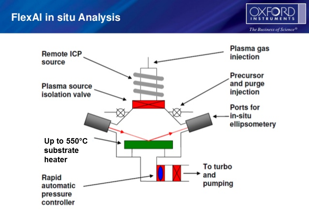
Basic set up of the FlexAL system including optional in-situ ellipsometry
Nickel oxide films have been demonstrated by plasma ALD, using nickelocene and oxygen plasma. Rapid bubbling of the precursor delivers efficient dosing, while low pressure O2 plasma allows for fast surface saturation and good uniformity.

Hafnium oxide films have been demonstrated by plasma ALD using tetrakis(dimethylamido)hafnium (TDMAH) and oxygen plasma. This results in improved deposition uniformity over tetrakis (ethylmethylamido) hafnium (TEMAH), even at short cycle times. Electrical characterisation of resultant HfO2 films will be discussed.

In general, the important parameters for plasma ALD of SiO2, NiO and HfO2 will be discussed, focusing on the effect of flow and pressure for each process step.

[1] G. Dingemans, C. A. A. van Helvoirt, D. Pierreux, W. Keuning, W. M. M. Kessels, E.C.S. 3 (2012) H277.
[2] T.S. Yang, W. Cho, M. Kim, K.-S. An, T.-M. Chung, C. G. Kim, Y. Kim, J. Vac. Sci. Technol. A 4 (2005) 1238.
[3] A. Colon, J. Shi, Solid-State Electronics 99 (2014) 25.

Tuesday, September 13, 2016

Plasma Electronic form Germany new sponsors of the BALD Engineering News Blog

I am very happy to announce that Plasma Electronic from Germany is now a sponsor of the BALD Engineering ALD News Blog. I met with Plasma Electronic during the ALD2016 Ireland conference end of July and hope to hear more about there progress with their wafer based PEALD reactor (see picture below) and other plasma processing technologies. One of the next chances to meet with Plasma Electronic will be at the Euro CVD-Baltic ALD 2017 Exhibition in Sweden next summer. Also you may check their news services here for additional announcements and exhibitions : http://www.plasma-electronics.com/news.html


Plasma Electronic at the ALD2016 Ireland exhibition demonstrating their PEALD technology to the conference delegates.

Plasma Electronic is specialized on the planning, design, construction and marketing of plasma treatment devices. The focus is the activation and fine cleaning of surfaces and the coating of surfaces with the technologies PECVD, PVD, PEALD and their combinations. In their laboratory they are able to measure and analyze properties of coatings like hardness, coating thickness, surface energy and surface tension.

The facility has a production area of 1000 m² enabling us to construct all sizes of plasma devices. The plasma chamber sizes vary from 10 liters in research and development devices up to 8000 liters in devices for mass production.

Plasma Electronic has developed a variety of processes for different applications. They can be used to remove residues of organic or silicone pollution (
Plasmaclean©), for better wettability and adhesion (Actiplas©), for permanently hydrophilic (Aquacer©) or hydrophobic (Lipocer©) coatings, for hard coatings with low wear and low friction (Carbocer©), for transparent protection and "anti-fingerprint" coatings (Clearprotect©) and for decorative coatings (Decocer©).

Plasma Electronics ALD Offerings

Sunday, September 11, 2016

Globalfoundries Fab 1 Dresden to start 12 nm FDSOI enabled by double patterning

Here is good news for the Globalfoundries Fab1 in Dresden and the many people I know working there! Fab1 has already successfully ramped 22 nm FDSOI by using Double Patterning in combination with Immersion lithography and will now according to a statement by Gregg Bartlett, senior vice president of the CMOS Platform Business Unit at GlobalFoundries continue with the same technology for 12 nm FDSOI:

When it comes to the patterning in lithography, “it’s very analogous on 22nm,” Bartlett said. The 22nm FD-SOI process involves double patterning, with two metal layers, and that’s the plan for 12nm, as well. “No triple patterning.” [Semiconductor Engineering]

PEALD is typically employed for double patterning this could mean some extra business for the OEMs supplying single wafer PEALD like ASM Internationals Eagle XP8 platform, which is also capable of PECVD that may be used for spacer/liner applications. Please find more details on the 12 nm FDSOI news below.

GLOBALFOUNDRIES unveiled a new 12 nm FD-SOI semiconductor technology, extending its leadership position by offering the industry’s first multi-node FD-SOI roadmap. Building on the success of its 22FDX™ offering, the company’s next-generation 12FDX™ platform is designed to enable the intelligent systems of tomorrow across a range of applications, from mobile computing and 5G connectivity to artificial intelligence and autonomous vehicles.

 Globalfoundries Fab1 in Dresden Germany (Wikipedia)

Thursday, September 8, 2016

Modular flow and Plasma Electronic from Germany to Exhibit at EuroCVD - Baltic ALD 2017

We are very happy to annonc that modular flow and Plasma Electronic from Germany to Exhibit at EuroCVD - Baltic ALD 2017 in Linköping Sweden 11-14 Junde 2017.

Please contatc us if you like to join the exhibition!

Henreik Pedersen (henrik.pedersen@liu.se)
Jonas Sundqvist (jonas.sundqvist@baldengineering.com)


Aug 15, 2016 ... modularflow launches mini ALD reactor with integrated QCM ... modularflow mini ALD Dimensions with 3 precursor sources: approx. 420 x 260 ...

Sunday, July 31, 2016

Trends in plasma-enhanced atomic layer deposition

The mysterious Plasma ALD Guy (PAG) had a great time at ALD 2016 this past week. PAG presented a poster on Tuesday evening that was enjoyed by many. If you missed it, you can check it out here.


Based on the review 2013 to 2015 South Korea is in the lead judging by the number of PEALD publications followed by USA and Germany. Striking is the lack of PEALD publications coming from the leading ALD centers of Helsinki University, VTT and Aalto University.

The other observation is that >75% of all PEALD is performed for pretty basic ALD materials (Al2O3, AlN, TiO2) using basic ALD precursors like TMA. The Finnish ALD community has a strong tradition of focusing on new precursor chemistries and new materials and that may be an explanation why PEALD is not in the focus there.

You also see that Turkey is very strong represented in this field. Unfortunately many of the Turkish Scientists were not allowed to participate in ALD2016.