Showing posts with label GAAFET. Show all posts

Friday, October 20, 2023

The Semiconductor Showdown: TSMC's GAA FETs vs. Intel's RibbonFET

The semiconductor industry is witnessing a fierce competition between TSMC and Intel, as they advance transistor designs with TSMC's Gate-All-Around (GAA) FETs and Intel's RibbonFET. Atomic Layer Deposition (ALD) plays an instrumental role in crafting these intricate designs. As the race to dominate the microelectronics realm heats up, the innovations from these giants foretell a transformative phase for technology between 2024 and 2026. This article dives into their respective technologies, comparing their strategies and highlighting the future implications for the semiconductor industry.

Both TSMC and Intel are pushing the boundaries of semiconductor innovation with advanced transistor designs. TSMC's GAA (Gate-All-Around) FET (Field-Effect Transistor) technology and Intel's RibbonFET are prime examples of this evolution. ALD is crucial for GAA FET production, ensuring precision and atomically thin, conformal or on purpose non-conformal or selectively deposited films. As transistors miniaturized, ALD replaced traditional silicon dioxide gate dielectrics with high-k materials, reducing gate leakage and offering enhanced uniformity. One of the challenges in GAA FETs is accurately aligning the gate material around the channel; ALD facilitates this through self-aligned processes. Additionally, in configurations with multiple gates or nanosheets, ALD accurately deposits spacer materials, preserving the necessary separation between nanosheets. ALD also offers precise doping for GAA FETs, including NMOS and PMOS. With atomic-level control, ALD introduces dopants like phosphorus for NMOS and boron for PMOS. Given the shrinking device dimensions, ALD's precision becomes vital, especially when considering techniques like solid-state doping to achieve ultra-shallow profiles.


TSMC's Gate-All-Around (GAA) FET technology represents a significant shift from the traditional FinFET transistor design. In a GAA FET, the gate material wraps entirely around the channel, unlike the FinFET where the gate is only on three sides of a vertical fin. This complete encirclement provides enhanced control over the current flow through the channel, reducing leakage current and allowing for lower voltage operation. The result is improved energy efficiency and performance.


TSMC's roadmap to N2. (Image: TSMC)

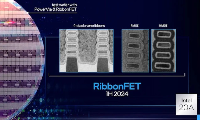
On the other hand, Intel's RibbonFET introduces a similar gate-all-around design but with a unique twist. Instead of a traditional vertical fin, RibbonFET uses nanosheet technology, where multiple flat nano-sheets are stacked to form the channel. This design offers even better control of the current flow, leading to significant gains in performance and efficiency. RibbonFET is one of Intel's flagship innovations for its advanced nodes, emphasizing the company's commitment to reclaiming technology leadership in the semiconductor space.


Intel 20A Ribbon FET (intel.com)

In a recent article Tom´s Hardware (Anton Shilow, link below) compares the advanced semiconductor technology nodes from industry TSMC and Intel, focusing on TSMC's N3P and N2 nodes against Intel's 20A and 18A nodes. Forecasted for release between 2024 and 2026, these nodes represent the forefront of semiconductor innovation. TSMC's N3P, a 3nm-class node, is set to be available by 2025 and offers performance comparable to Intel's 18A. Interestingly, TSMC's 2nm-class N2, expected in the second half of 2025, is anticipated to outpace Intel's 18A in terms of power, performance, and area advantages. Intel's 20A, arriving in 2024, promises significant advancements by introducing RibbonFET gate-all-around transistors and a backside power delivery network. The subsequent 18A will further refine these innovations. While TSMC leans on its proven FinFET technology for the N3P, it plans to introduce nanosheet GAA transistors in the N2. 

As the semiconductor race intensifies, both companies are heavily invested in outpacing each other, with TSMC focusing on technology maturity and cost-effectiveness, and Intel aiming to regain its technology leadership. The dynamics between these tech giants will shape the semiconductor industry's future.


Comparison of Advanced Semiconductor Technology Nodes: TSMC N3P & N2 vs. Intel 20A & 18A, highlighting the competitive landscape of the semiconductor industry for the years 2024-2026 based on Toms Hardware article below.

Sources: 

TSMC: Our 3nm Node Comparable to Intel's 1.8nm Tech | Tom's Hardware (tomshardware.com)

Intel and TSMC company web pages

Saturday, June 12, 2021

Applied Materials to present New Innovations Needed to Continue Scaling Advanced Logic (June 16)

Applied Materials (Santa Clara, USA): The semiconductor industry is at a crossroads. Demand for chips has never been greater as we enter the early stages of a new wave of growth fueled by the Internet of Things, Big Data and AI. At the same time, it’s become apparent that conventional Moore’s Law 2D scaling techniques are no longer able to deliver the consistent improvements in power, performance, area-cost and time to market (PPACt) that chipmakers have long relied on. This is particularly the case for logic chips, which serve as the main processing engine in nearly every electronic product and where power efficiency and performance are critical.

To shed light on this issue, Applied Materials is hosting an online Logic Master Class on Wednesday, June 16. I will be joined by other experts from Applied and the industry to discuss the logic scaling roadmap, including challenges and solutions for delivering continued improvements in PPACt. We will be exploring several different areas, including transistor and interconnect scaling, patterning and design technology co-optimization (DTCO). The common denominator underlying all of these areas is the need to supplement classic 2D scaling with a combination of approaches that includes new chip architectures, new 3D structures, novel materials, new ways to shrink features and new ways to connect chips with advanced packaging.

Source: Applied Materials Blog (LINK)


Primary modules of a FinFET are channel and shallow trench isolation (1), high-k metal gate (2) and transistor source/drain resistance (3). (Credit: Applied Materials)

Thursday, November 19, 2020

Intel to present 3D stacked Nanoribbon Transistors for Continued Moore’s Law Scaling at IEDM 2020

Intel to present stacked gate-all-around FET (GAA-FET) technology, i.e., a complementary FET (CFET) at IEDM2020. In CFETs, the idea is to stack both nFET and pFET wires on each other. A CFET could stack one nFET on top of a pFET wire, or two nFETs on top of two pFET wires. This ‘folding’ of the nFET and pFET eliminates the n-to-p separation bottleneck, reducing the cell active area footprint (LINK). Please find the announcement below:

Home-2020 - IEDM 2020 ieee-iedm.org IEDM Conference 2020. To Be Held Virtually December 12-18. The on demand portion of the conference will begin on December 5th. Intel to present 3D stacked Nanoribbon Transistors for Continued Moore’s Law Scaling: 

Stacked NMOS-on-PMOS Nanoribbons: From planar MOSFETs, to FinFETs, to gate-all-around (GAA) or nanoribbon devices, novel transistor architectures have played a critical role in driving performance predicted by Moore’s Law. Intel researchers will describe what may be the next step in that evolution: NMOS-on-PMOS transistors built from multiple self-aligned stacked nanoribbons. This architecture employs a vertically stacked dual source/drain epitaxial process and a dual metal gate fabrication process, enabling different conductive types of nanoribbons to be built so that threshold voltage adjustments can be made for both top and bottom nanoribbons. The approach combines excellent electrostatics (subthreshold slope of <75 mV/dec) and DIBL (<30mV/V for gates ≥30nm) with a path to significant cell size reduction due to the self-aligned stacking. These devices were used to build a functional CMOS inverter with well-balanced voltage transfer characteristics. (Paper #20.6, “3-D Self-Aligned Stacked NMOS-on-PMOS Nanoribbon Transistors for Continued Moore’s Law Scaling,” C.-Y. Huang et al, Intel) 

Paper #20.6, “3-D Self-Aligned Stacked NMOS-on-PMOS Nanoribbon Transistors for Continued Moore's Law Scaling,” C.-Y. Huang et al, Intel

Paper Information (IEDM 2020) : LINK

Figures from IEDM 2020 Press briefing Material -Press kit : LINK

In the images above:

·        (1) shows the evolution of transistor architectures from planar, to FinFETs, to nanoribbons and to a 3D CMOS architecture.

·        (2) (a) shows a 3D schematic diagram of stacked CMOS Si nanoribbon transistors with NMOS on PMOS, (b) describes the process flow; (c) is a TEM image of a stacked multiple-nanoribbon CMOS inverter with a 40-nm gate length and inner (Vss) and outer (Vcc) contacts, a common gate input (VIN) and an inverter output node (VOUT); while (d) is a TEM image of two Si NMOS nanoribbons atop 3 Si PMOS nanoribbons.

·       (3) (a) is a process flow of the vertically stacked dual S/D EPI process, while (b) shows P-EPI selectively grown on the bottom three nanoribbons, (c) shows N-EPI selectively grown on the top two nanoribbons, and (d) features TEM and EDS images showing selective N-EPI and P-EPI growth on the stacked nanoribbon transistors.

·       (4) (a) is a process flow of the vertically stacked dual metal gate process; (b) is a TEM image and (c, d) are EDS images of the dual metal gate with N-WFM (WFM = work function metal) on the top two nanoribbons and P-WFM on the bottom three nanoribbons.


Saturday, January 4, 2020

Samsung's 3 nm Gate-All-Around FET prototype

Samsung has succeeded in making the first strides towards the 3 nm process, as reported by the Korean Maeil Economy this week. According to the report, Samsung's goal is to become the world's number one semiconductor manufacturer by 2030.

Samsung's work on the 3 nm process is based on the Gate All Around (GAAFET) technology rather than FinFET. This supposedly reduces the total silicon size by 35% while using about 50% less power and allows for the same amount of power consumption and 33% performance increase over the 5 nm FinFET process.


Gate-All-Around FETs - Picture credit: Samsung

Source: Toms Hardware (LINK)

----------
By AbhishekkumarThakur