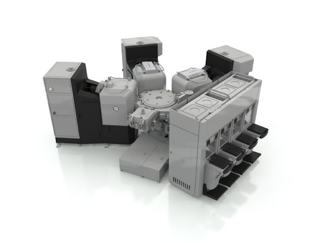
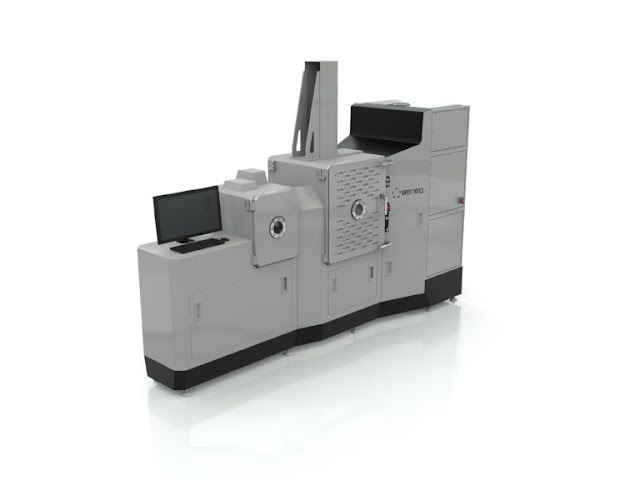
Showing posts with label Beneq. Show all posts

Wednesday, December 27, 2023

Exploring Ultrathin Solar Cells with Professor Carl Hägglund: A Journey from Stanford's ALD Techniques to Plasmonic Solar Cell Optimization

In this episode, Tyler is joined by Professor Carl Hägglund from Uppsala University. They discuss Carl’s motivations for pursuing ultrathin solar cells, how he learned ALD at Stanford in Stacey Bent’s lab, and an unlikely research connection through his child’s school. They also talk about why ALD is useful for plasmonic solar cells, optimization of SnS ALD and his planned path towards a fully realized ultrathin photovoltaic.


00:00 Introduction
01:45 Motivation for fabricating plasmonic solar cells
09:58 Learning ALD at Stanford
22:46 Optimizing SnS ALD process
30:33 Path towards an ultrathin solar cell

Tuesday, August 22, 2023

Beneq invites you to ALD TechDay during SEMICON Europa 2023

Beneq invites you to ALD TechDay during SEMICON Europa 2023 in Munich this November! Discover the latest trends and applications in Atomic Layer Deposition (ALD) for specialty semiconductors. Industry leaders and experts will share insights on ALD adoption and its impact.

Don't miss this exclusive forum brought to you by SEMI and Beneq. Register now!


Friday, June 2, 2023

Finnish ALD equipment manufacturer Beneq has entered a partnership with Lung Pien Vacuum Industry Co., Ltd. in Taiwan.

Finnish ALD equipment manufacturer Beneq has partnered with Taiwan's Lung Pien Vacuum Industry to promote ALD technology for optical applications. They held a seminar to exchange knowledge and explore ALD solutions for mass production challenges. ALD is a process that deposits atomic thin films with advantages like large-area coverage and precise film thickness control. Beneq, a global leader in ALD equipment, introduced AtomGrassTM ALD, a wide-angle broadband anti-reflective coating. Lung Pien will provide Beneq's equipment and services to its optics customers in the Asia-Pacific region. The partnership aims to actively promote ALD coating technology for high-end curved lenses in Taiwan's optical market.

Finnish ALD equipment manufacturer Beneq has formed a partnership with Lung Pien Vacuum Industry, a prominent vacuum coating equipment manufacturer based in Taiwan. The collaboration aims to promote ALD technology for emerging optical applications, such as camera lenses for mobile phones and automobiles. In April, the two companies organized an "ALD Optical Coating" seminar in Taiwan, inviting major optical manufacturers to exchange knowledge and explore ALD solutions for mass production challenges. ALD is a deposition process that involves the formation of self-limited reactions between precursor gases and a substrate surface, resulting in atomic thin films with advantages like large-area coverage, high step coverage, low-temperature processing, and precise film thickness control.


Peter Hsieh (left standing), Beneq’s Advanced ALD Sales Director, and Kalle Niiranen (right standing), Technical Sales Manager, hosting the ALD Optical Coating seminar on the 20th of April in Taichung, Taiwan.

Beneq has been a pioneer in industrial ALD production since 1984 and has established itself as a global leader in ALD equipment manufacturing. The company offers a wide range of technical products and R&D services, with a focus on finding industrial ALD solutions through collaboration and co-development. Beneq recently introduced AtomGrassTM ALD, an innovative wide-angle broadband anti-reflective (AR) coating. This solution provides exceptional anti-reflective properties with less than 0.07% average reflectance across a wide wavelength range and significantly improves performance at high angles of incidence.

According to Peter Hsieh, Sales Director of Beneq's Advanced ALD Business Unit, the demand for ALD is increasing in the nano-processes of the integrated circuit industry. ALD has replaced traditional methods like CVD and PVD for many key thin-film processes. Hsieh believes that ALD's development is now closer to industrial-grade 12-inch mass production equipment, opening up excellent application opportunities in various fields, including optoelectronics, automotive, medical materials, and more.

Lung Pien Vacuum Industry, founded in 1991, has a longstanding relationship with the optical industry. The company offers a comprehensive range of services, including product design, development, equipment manufacturing, production planning, operator training, and process design consulting. While Lung Pien primarily focuses on vacuum evaporation and sputtering equipment manufacturing, thin film process technology services, and other related products, their partnership with Beneq will enable them to provide Beneq's ALD equipment and services to their extensive network of optics customers in the Asia-Pacific region. The collaboration between Beneq and Lung Pien aims to actively promote ALD coating technology for high-end curved lenses in Taiwan's optical market, leveraging ALD's ability to provide uniform conformal thin film layers for complex structures.

Monday, September 26, 2022

Atomic Layer Deposition (ALD) - Compound Semiconductor magazine interview with Beneq

Richard Stevenson, Editor of Compound Semiconductor magazine, talks to Mikko Söderlund, Beneq's Head of Sales for its Semiconductor ALD Business Unit, about the phenomenal interest in this sector.


Compound Semiconductor Magazine: www.compoundsemiconductor.net
Beneq's Semiconductor ALD Business: www.beneq.com/en/products/semiconductors


Friday, June 10, 2022

Atomic Layer Deposition Expected to Grow to Meet Demand for More-than-Moore Devices and Applications

(Interview by SEMI) Atomic Layer Deposition (ALD) players are poised to seize a new growth opportunity after the chip shortage pushed manufacturers to announce fab capacity expansions worldwide. Geared toward 200mm market needs, 300mm ALD platforms have recently advanced to meet the demand of More-than-Moore (MtM) devices and applications for MEMS, sensors, power and RF devices, photonics. Driven by the wafer production volume increase, ALD solutions are now expected to grow and enter the MtM devices market.


SEMI spoke with Dr. Patrick Rabinzohn, Strategic Development Executive of Semiconductor ALD at Beneq, about the benefits of ALD and shared how Beneq is building a comprehensive ALD product portfolio – from Beneq Transform® to ProdigyTM – covering different device applications and wafer sizes. We also talked about Beneq solutions to customer challenges, thanks to its vision and future trends for MtM devices for ALD.

SEMI: Beneq is already a familiar name in the ALD equipment business. For those new to the brand, please introduce the company.

Rabinzohn: Beneq is the home of atomic layer deposition and has ALD in its DNA. In fact, the very first industrial application of ALD was done in 1984 here on electroluminescent displays – the same location where Beneq still is headquartered today! Beneq was formed in 1984 and today we are a leading provider of ALD solutions for More-than-Moore semiconductor device fabrication with the Beneq Transform®.

Beneq’s state of art applications lab enables proof-of-concept and customer adoption for new ALD processes. Our team of engineers and experts is dedicated to making ALD tools accessible to our customers and partners.

SEMI: Beneq introduced the first Beneq Transform® in late 2019. How has adoption been so far?

Rabinzohn: The Beneq Transform® has revolutionized ALD cluster tools for More-than-Moore semiconductor markets in the EU, the U.S. and Asia since its launch in 2019. As of November 2021, Beneq has seen higher than expected demand for both the Transform and Transform Lite product configurations across key customer regions such as Europe, Japan, China, Taiwan and the U.S. We are super excited to see more customers adopting ALD in their More-than-Moore applications.

Tuesday, April 5, 2022

Using Vapor Phase Infiltration for Fabricating Membranes with David Bergsman – ALD Stories Ep 11


From the corner of one continent to another, Professor David Bergsman joins Tyler from the University of Washington in Seattle. David discusses his use of vapor phase infiltration as a method of fabricating new membrane structures inspired by his work in Stacey Bent’s lab at Stanford and how he started an ALD lab during a pandemic. 
In this video: 
00:00 – Introduction 
02:01 – David’s Background & MLD 
08:02 – Membrane Fabrication and Property Challenges 
17:19 – Vapor Phase Infiltration 
37:36 – Starting an ALD lab 
48:30 – Ending & Outro 

Follow Professor David Bergsman on Twitter @DavidBergsman and learn about his research group in Seattle at www.bergsmangroup.com

Innovative Spatial ALD system at the LZH can precisely coat complex-shaped optics

New possibilities: The LZH can also coat curved optics uniformly with the innovative Spatial ALD system. This is interesting, for example, for applications in the automotive lighting sector. The system achieves high deposition rates.Thanks to the plasma-based Spatial ALD system, another application that is in high demand in industry has been made economical. Layer systems of uniform thickness can be developed and manufactured much faster than before on curved and structured optics.

The system was developed by the Finnish company Beneq together with the LZH.


Thursday, March 10, 2022

Beneq fulfills customer demand for tailored ALD equipment services and support with BeneqCareTM

Beneq, the home of Atomic Layer Deposition (ALD), has introduced BeneqCare, a new modular solution to offer support and maintenance services to organizations that own and operate Beneq ALD equipment.

Beneq leads the market with ALD products for R&D, semiconductor device fabrication, 3D and batch production, ultra-fast spatial ALD (C2R), and roll-to-roll ALD. Today, the company has launched BeneqCare to help customers in the EU, Asia and the USA maximize the value of their ALD tools throughout their equipment’s life cycles.


“We have been investing heavily in widening our service capabilities worldwide. Now, we offer service coverage in all regions. We have also established spare part hubs in every region at Beneq offices,” says Hans Fabritius, Vice President, Life Cycle Services at Beneq.

“BeneqCare simplifies ALD equipment ownership by helping our customers maximize uptime and gain access to the right support at every stage of their tool’s life cycle. We are ready to assist our customers in meeting their productivity requirements –from training personnel in using the equipment to meeting any unscheduled maintenance or spare parts needs,” asserts Fabritius.

BeneqCare provides Beneq customers who operate in the industrial and research sectors with a wide range of service modules to suit their operations, from extended warranty and training services to remote or onsite support.

“Our customers have high expectations for the performance of their Beneq ALD tools. BeneqCare brings them versatile support and service plans that grow with their businesses,” says Fabritius.

Companies and research facilities that have commissioned Beneq ALD equipment can avail of a variety of BeneqCare service modules to suit their unique requirements. Among the BeneqCare modules are technical support services, including remote support via Augmented Reality (AR); spare part services; extended warranties; preventive as well as unscheduled maintenance services; and training.

Learn more about BeneqCare.


Tuesday, December 7, 2021

Beneq unveils two new ALD products for 300mm and compound semiconductor device fabrication respectively

Beneq revolutionized ALD cluster tools for More-than-Moore device makers with the highly successful Beneq Transform® family of products. Today, Beneq broadens its product portfolio further with two new distinct solutions: the Transform® 300 and ProdigyTM.

The Beneq Transform 300 and Prodigy were each created in response to specific technology requirements in the semiconductor manufacturing sector.

“The Transform 300 is designed to meet the growing demand of emerging semiconductor applications at 300 mm for devices such as CMOS image sensors, Power Devices, Micro-OLED/LED, and Advanced Packaging, which call for a high degree of versatility,” explains Patrick Rabinzohn, Vice President, Semiconductor ALD at Beneq.

“We created Prodigy to address those market segments that need a simple solution supported by high-end technology. It inherits the ALD design and processing knowhow we at Beneq have developed over the last 15 years, packing advanced features in a simpler, targeted industrial form factor,” continues Rabinzohn.
Beneq Transform 300 is the only 300 mm ALD cluster tool that combines thermal ALD (batch) and plasma ALD (single wafer) technologies to provide a highly versatile platform for IDMs and foundries. It is dedicated to advanced thin-film applications in CIS, Power, Micro-OLED/LED, Advanced Packaging and other MtM applications.

Beneq Tranform 300 is a highly configurable platform that caters to multiple advanced thin-film applications ranging from gate dielectric including in high aspect ratio trenches, to anti-reflection coating, final passivation or encapsulation, Chip-Scale-Packaging and beyond.

Beneq Prodigy is the deal manufacturing solution for compound semiconductor including RF IC’s (GaAs/GaN/InP), LED, VCSEL, Light Detectors and for MEMS manufacturers and foundries looking to enhance device performance and reliability through an affordable stand-alone ALD batch tool. Beneq Prodigy provides best-of-breed passivation and encapsulation films across multiple wafer types and sizes.

To learn more, visit:


Friday, November 19, 2021

How Did Plasmas Change ALD? - w/ Erwin Kessels (ALD Stories Ep 8)

In Episode 8 of ALD Stories, Tyler chats with Eindhoven University of Technology professor, Erwin Kessels, about plasma-enhanced ALD, industry applications, and Erwin's Atomic Limits blog & teaching strategies. 

In this video: 
00:00 - Intro
  01:46 - PEALD Basics, Ions, & Applications 
20:56 - Semiconductor Industry Advantages 
28:05 - Photovoltaic Passivation 
36:43 - Atomic Limits Blog & Teaching 
45:25 - Outro 

Professor Erwin Kessels - https://www.tue.nl/en/research/resear... 
Atomic Limits Blog - https://www.atomiclimits.com/


Thursday, September 30, 2021

ALD Stories Ep 6 - ALD Precursor Design for Hard to Deposit Metals with Prof. Chuck Winter

Tyler sits down with Wayne State University’s Chuck Winter to talk about his approach to designing precursors for ALD. Chuck explains what makes a good ALD precursor and how elegant organic chemistry can enable ALD processes for hard-to-deposit metals, like cobalt and aluminum. 

Learn more about Chuck’s research here: http://www.clas.wayne.edu/wintergroup/ 

Papers mentioned in this episode: 


Friday, September 3, 2021

The world’s largest ALD system - The BENEQ P1500 is here!

Now it is here - The Beneq P1500 is the biggest ALD system and is built specifically to coat sizeable sheets and complex parts. It is also made to deliver increased throughput for batches of smaller components.


Beneqs customers use the P1500 for optical coatings on large diameter substrates, anticorrosive coatings of semiconductor equipment parts, and various applications where ALD is used on glass or metal sheets.


Large parts need large ALD tools. The Beneq P1500 can accommodate parts up to 1300 × 2400 mm in size, and enables the deposition of high-quality, functional optical coatings on wide area mirrors or lenses. It is also used to coat batches of parts in the 300 to 1000 mm size range.

More information: LINK


Thursday, April 15, 2021

BENEQ P800 coating batches of 300 mm showerhead plates for advanced semiconductor wafer processing equipment

How it is done - Here a cool video of a BENEQ P800 coating 300 mm showerhead plates for some advanced semiconductor wafer processing equipment.


Friday, April 9, 2021

BENEQ P800 Upgrade - Proven Batch ALD for High Volume Production

BENEQ has freshened up its true ALD workhorse the P800 Batch reactor, which probably has the biggest load size in the industry.


PDF Product description for download: LINK


Tuesday, March 9, 2021

ALD Stories podcast with Dr. Katja Väyrynen, Process Development Engineer at Beneq

On this episode of the ‘ALD Stories’ podcast, We speak to Dr. Katja Väyrynen, Process Development Engineer at Beneq. What is the latest ALD research on improving the performance of microchips? Will cobalt become a popular material in semiconductor manufacturing? Hear her journey from the video above and read more about ALD Stories here: https://beneq.com/en/podcast/


Tuesday, January 19, 2021

Webinar - Enhancing Yield by Minimizing Contamination with Beneq ALD coating solutions

Yet another Webinar with Beneq, this time about ALD coating solution for your equipment.

Regsitration: LINK


Semiconductor manufacturing involves corrosive gases in multiple processes. As we transition to each new technology node, e.g. from 10nm to 7nm and to 5nm, there are even more stringent fab requirements against metal and particle contamination. This poses challenges for existing coating methods such as anodization or plasma spray, which may not provide complete protection especially on critical chamber components with complex geometry. 

This webinar is particularly helpful for process engineers, equipment engineers and others, who are responsible for contamination control and equipment yield. 

Learn more about :
  • Common issues of metal or particle contamination on critical chamber components 
  • Common coating methods against corrosion, and how they compare 
  • What properties to look for e.g. purity, uniformity, when evaluating the optimal protective coating solution 
  • Unique benefits of ALD coatings with Al2O3 and Y2O3 
  • Working with your OEM partner to design, test and implement an ALD coating solution for your equipment

Thursday, December 17, 2020

Beneq completes new clean room facility

The new ISO 7 cleanroom will be dedicated to manufacturing ALD equipment for semiconductor and other markets with similar cleanroom requirements. The new Espoo, Finland facility includes a 350 m2 ISO 7 cleanroom and a 150 m2 ISO 5 semiconductor ALD application laboratory. 


Beneq, a supplier of atomic layer deposition (ALD) equipment for semiconductor and other industrial markets, has completed construction of a brand-new cleanroom and application laboratory at its corporate headquarters in Espoo, Finland. 

Built with the latest cleanroom design and construction technology, the new facility adds approximately 350 square meters of ISO 7 cleanroom floor space at Beneq's headquarters. It will be used for product and process development, equipment assembly, prototyping, and testing services. 
 

"Since the launch of the Beneq TransformTM last year we have seen great demand for our ALD equipment products from semiconductor customers,” stated Dr. Tommi Vainio, Vice President of ALD at Beneq. “Together with the semiconductor application laboratory the new cleanroom will be the engine for Beneq’s rapid growth in More-than-Moore markets, including power semiconductors, RF, image sensors, MEMS, compound semiconductors, LED & Micro-LED, OLED, and more.” 

The new cleanroom is part of Beneq’s ISO 9001 certified processes. It also houses a modern 150 square-meter semiconductor application laboratory, solely designed for developing and prototyping ALD solutions for More-than-Moore applications. Beneq has also expanded its existing cleanroom facility to ensure the highest availability and new safety features. 

The new cleanroom officially entered into production in December 2020. Prior to this facility the company had 1900 square meters of existing cleanroom capacity, which it will continue to operate for other customer markets.

Thursday, December 10, 2020

ALD Webinar - The Ultimate Anti-Corrosion Coating Solution presented by Beneq

Join this webinar featuring ALD (atomic layer deposition) pioneer Beneq to learn about the unique benefits of ALD for critical chamber components with complex geometry, and how the technology offers the ultimate anti-corrosion coating solution for semiconductor equipment parts.

Wednesday, January 27, 2021, 9:00 AM – 10:00 AM CET


If you can't attend the live session, register for access to a recording for later viewing.


Semiconductor manufacturing involves corrosive gases in multiple processes. As we transition to each new technology node, e.g. from 10nm to 7nm and to 5nm, there are even more stringent fab requirements against metal and particle contamination. This poses challenges for existing coating methods such as anodization or plasma spray, which may not provide complete protection especially on critical chamber components with complex geometry. 

Topics to be discussed:
  • Common issues of metal or particle contamination for critical chamber components
  • Common coating methods to protect against corrosion, and how they compare
  • What properties to look for – e.g. high purity and uniformity – when evaluating the optimal protective coating solution
  • Unique benefits of ALD coatings with Al2O3 and Y2O3
  • How to work with your OEM partner to design, test and implement an ALD coating solution for your equipment

Agenda and Speaker Information

Sponsored by


Tuesday, November 10, 2020

ALD and Nanotubes on Beneq ALD Stories

In Episode 3 of ALD Stories, we meet with Professor Jan Macak from the University of Pardubice. Hear and see his findings on ALD as an exceptional way to tailor the functionality of nanostructures, and the overlooked steps for making the perfect TiO2 nanotube.