Thursday, March 31, 2016

Precursor saving ALD Method from University of Alberta

Here is a clever paper from University of Alberta on how to save expensive ALD precursor in ALD processing by using a burst of  shorter multiple precursor pulses. I´ve seen this approached used in 3D conformal growth in extreme high aspect ratio structures before, but I just had a simple picture in my mind how it works. Here it is explained an proven by experimental work in great detail! 

The approach is also in one sense similar to the Genus process that ran the ALD pulses in undersaturation and was very much faster and precursor saving than "normal ALD". However not that good in extreme aspect ratio structures. The method developed by Triratna Muneshwar should not have this restriction since it works in saturation mode.


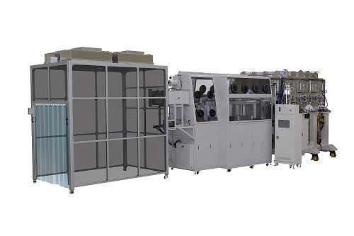
University of Alberta materials engineering postdoctoral fellow Triratna Muneshwar and materials engineering professor Ken Cadien have developed a new method for ALD that saves expensive precursors. The paper in Journal of Applied Physics is highlighted here in EurekAlert. On the picture the gentlemen stands in front of a ALD machine from Kurt J. Lesker, which I assume has been used for the experimental verification of the numerical method.

AxBAxB… pulsed atomic layer deposition: Numerical growth model and experiments

Triratna Muneshwar and Ken Caddie
J. Appl. Phys. 119, 085306 (2016); http://dx.doi.org/10.1063/1.4942439

Atomic layer deposition(ALD) is widely used for the fabrication of advanced semiconductor devices and related nanoscale structures. During ALD, large precursor doses (>1000 L per pulse) are often required to achieve surface saturation, of which only a small fraction is utilized in film growth while the rest is pumped from the system. Since the metal precursor constitutes a significant cost of ALD, strategies to enhance precursor utilization are essential for the scaling of ALD processes. In the precursor reaction step, precursor physisorption is restricted by steric hindrance (mA1) from ligands on the precursor molecules. On reaction,some of these ligands are removed as by-products resulting in chemisorbed species with reduced steric hindrance (mA1 → mA2, where mA2 < mA1) and some of the initially hindered surface reaction sites becoming accessible for further precursor physisorption. To utilize these additional reaction sites, we propose a generalized AxBAxB… pulsed deposition where the total precursor dose (ΦA) is introduced as multiple x (x > 1, x ∈ I) short-pulses rather than a single pulse. A numerical first-order surface reactionkinetics growthmodel is presented and applied to study the effect of AxBAxB… pulsed ALD on the growthper cycle (GPC). The model calculations predict higher GPC for AxBAxB… pulsing than with ABAB… deposition. In agreement with the model predictions, with AxBAxB… pulsed deposition, the GPC was found to increase by ∼46% for ZrN plasma enhanced ALD (PEALD), ∼49% for HfO2 PEALD, and ∼8% for thermal Al2O3ALD with respect to conventional ABAB… pulsed growth.

Wednesday, March 30, 2016

Picosun’s ALD solutions at Imec transform battery technology

ESPOO, Finland, 30th March, 2016 – Picosun Oy, the leading supplier of advanced ALD (Atomic Layer Deposition) thin film coating technology, now provides ALD equipment to transform battery manufacturing. 
 
The sustainable energy economy of the future, greener transportation, and the increasing number of portable, mobile and personal electronic devices all require improved means for local energy storage. Nanostructured, solid-state thin film batteries offer a disruptive solution for this. Replacing traditionally used liquid materials in the battery with all solid layers improves the battery safety and lifetime. Thin and flat geometry makes the batteries easily integrated in e.g. wearable electronics, whereas their nanoscale tailored internal structure enables high energy storage capacity.

ALD is an ideal way to prepare the highly conformal, dense, uniform, and structurally and chemically exactly controlled functional layers in the core of the battery stack. Using PICOSUN™ ALD equipment, imec, Belgium, has now developed a solution to deposit a novel, solid electrolyte for lithium ion thin film batteries.

“Our aim at Picosun is to utilize ALD technology for better tomorrow. For example, faster and smoother data handling and communications, and the increasing number of mobile, wearable personal health monitoring devices require compact, efficient, and reliable power delivery solutions. The ALD technology we have now developed with imec for manufacturing of safe and long-lasting thin film batteries is an important breakthrough into a huge market area still relatively new to ALD. We are happy to provide the latest manufacturing solutions to our customers in this field and to see their most advanced products powering our everyday electronics,” states Juhana Kostamo, Managing Director of Picosun.

Tuesday, March 29, 2016

Atomic/Molecular Layer Deposition of Lithium Terephthalate for Li-Ion Battery Anodes

EurekAlert.org reports: When microbatteries are manufatured, the key challenge is to make them able to store large amounts of energy in a small space. One way to improve the energy density is to manufacure the batteries based on three-dimensional microstructured architectures. This may increase the effective surface inside a battery- even dozens of times. However, the production of materials fit for these has proven to be very difficult.


Aalto University Researchers testing the material on coin cells. (Mikko Raskinen / Aalto University)

Researches at Aalto University, Helsinki Finland, has develooped a ALD/MLD deposition process for Li-terephthalate, which has been published in Nanoo Letters (below).

- ALD is a great method for making battery materials fit for 3D microstructured architectures. Our method shows it is possible to even produce organic electrode materials by using ALD, which increases the opportunities to manufacture efficient microbatteries, says doctoral candidate Mikko Nisula from Aalto University. (EurekAlert.org)

Atomic/Molecular Layer Deposition of Lithium Terephthalate Thin Films as High Rate Capability Li-Ion Battery Anodes

Nano Lett., 2016, 16 (2), pp 1276–1281


We demonstrate the fabrication of high-quality electrochemically active organic lithium electrode thin films by the currently strongly emerging combined atomic/molecular layer deposition (ALD/MLD) technique using lithium terephthalate, a recently found anode material for lithium-ion battery (LIB), as a proof-of-the-concept material. Our deposition process for Li-terephthalate is shown to well comply with the basic principles of ALD-type growth including the sequential self-saturated surface reactions, a necessity when aiming at micro-LIB devices with three-dimensional architectures. The as-deposited films are found crystalline across the deposition temperature range of 200–280 °C, which is a trait highly desired for an electrode material but rather unusual for hybrid inorganic–organic thin films. Excellent rate capability is ascertained for the Li-terephthalate films with no conductive additives required. The electrode performance can be further enhanced by depositing a thin protective LiPON solid-state electrolyte layer on top of Li-terephthalate; this yields highly stable structures with capacity retention of over 97% after 200 charge/discharge cycles at 3.2 C.

Monday, March 28, 2016

NCD, a fast growing Korean ALD Equipment manufacturer for High Volume manufactuiring


As announced some weeks ago I am happy to have NCD as sponsor for the BALD Engineering ALD News blog. Here a review of the company and its fantastic ALD products follows and you should check the recently updated web page (http://www.ncdtech.co.kr/). NCD Co., Ltd. from Daejeon in Korea is a young and growing company founded in 2010 and is specialized in ALD original equipment manufacturing, which has been covered here on the ALD blog previously (here).


NCD is focusing on equipment development, process development, coating services, and process consulting for advanced ALD technologies for four business areas:

1. Solar
2. Display
3. Semiconductor
4. R&D

NCD has already had quite some successful years in entering the ALD equipment market and has built a very impressive customer base in Asia with main focus on the Korean domestic market, Japan, China and Taiwan.

As you may know, one of disadvantages of ALD is slow growth rate at typically an Å / cycle or so, that is to say ALD has a low throughput. In order to solve this problem, NCD has applied for patents for the high-throughput, high-volume and large-area every year. Based on these patents, NCD have developed their high-volume and large-area ALD system.

Here follows an overview of the ALD technology and equipment offering by NCD

1) High-volume ALD
   - GS ALD : surface passivation for c-Si solar cell                                                                         
   - MC ALD : dielectric for capacitor and encapsulation for micro display (OLED)

2) Large-area ALD
   - TS ALD : buffer layer for CIGS solar cell
   - GD ALD : encapsulation for OLED
LucidaTM GS1200 ALD with automation system

NCD has paved the way for high volume manufacturing by a range of ALD systems (see above). Worth highlighting here is especially the Lucida™ GS1200 ALD system applied for high efficiency solar cells at both Hyundai Heavy Industries and LG Electronics etc. The GS series from NCD can realize Passivation for c-Si solar cell at an impressive through put of >3400 wph @ 10nm-Al2O3.

For the large area CIGS thin film soar and OLED display market, NCD has developed two main platforms - the TS and the GD series respectively. ALD chamber clustering is an approach used by many rather than large stand-alone batch tools. 
LucidaTM GD600 ALD in R&D Lab.

Lucida™ GD series already had been applied to R&D centers of Korean and other customers, and showed the excellent performance for thin film encapsulation (TFE) and barrier applications. NCD is currently possible to run customer demoes with the large size of panel (1500mm x 1800) for using LucidaTM GD600 in the demo room (see above). NCD is the only place to do superior ALD demoes with that size panel.

It will be very exciting to follow NCD the next years when the ALD market continues its growth in many high-volume and large-area ALD applications.

Sunday, March 27, 2016

UHV PEALD system from AdNaNoTek

Here is a company for ALD that I was not aware of before that I came across while surfing internet. AdNaNoTek's is building all types of UHV Deposition Systems for MBE, PLD, IBSD, Sputtering, E-beam Evaporatioon, Thermal Evaporatioon, etc. and are now also offering a PEALD system.  Below is some information available from their web: LINK


Plasma Enhanced Atomic Layer Deposition (PEALD - 6)

AdNaNoTek's Plasma Enhanced Atomic Layer Deposition (PEALD - 6) can deposit epitaxial thin-film with extremely high quality and repeatability. This PEALD system is specially equipped with microwave plasma generator which produces plasma from successive ionization, vibrational excitation, and collision. Sufficient precursor units are provided to introduce deposition materials unto the substrate using a sophisticated gas control panel. The deposition chamber and substrate manipulator provides precise control of vacuum condition and substrate temperature to ensure epitaxial deposition process.


In addition, precise control and high stability is achieved by making the process automated with the use of the FBBEAR control software. The FBBEAR control software, provides complete data logging, precise parameter tuning  which allows user to have easy operation and reliable experimental repeatability.

PEALD can be applied for thin layer deposition of materials like: Silicon, Silicon oxide, etc.

MAIN SPECIFICATIONS (under construction):
  • Cylindrical SS316L electropolised chamber (1E-10 Torr)
  • 8-inch quick access door
  • 4-axis (XYZR) Laser heating sample manipulator (20 mm xy motion, 100mm z motion, continuous 360° rotation)
  • 1-inch sample holder (size upto 6-in)
  • Heating temperature up to 1000°C ± 1°C (in 1 atm O2 or O3 process gas)
  • High pressure RHEED system (real-time epitaxy monitoring)
  • Turbo pump with rough pump
  • Metal leak valves
  • Full range vacuum gauge
  • Industrial computer with 23" touchscreen
  • Full system control software (FBBear)
  • Large space with many ports for versatile expansion/upgrades
  • HV Load lock SS304 electropolished chamber (1E-7 Torr) with full range vacuum gauge and turbo pump

Saturday, March 26, 2016

New cyclic azasilanes as volatile and reactive precursors for ALD of SiO2 from Gelest


Here is a very good publication brought to my attention by Henrik Pedersen on Twitter. It is a nice screening exercise of a new class Si precursors for ALD of SiO2 using ozone fom Gelest Inc. SiO2 is one of the most important materials today in the 2nd ALD boom besides silicon nitride. 

As reported earlier here the equipment market for ALD single and multi wafer tools is expected to reach $1.2 billion in the next 2-3 years. One of the reasons behind tremendous growth expectation  is that LPCVD and PECVD just can´t meet the requirements of conformal growth and low thermal budget required by the sub 20 nm Logic and Memory technologies and especially for multi-patterning and also due to the 3D path of 3DNAND. One additional challenge that has to be confronted is to have a stable process that is not affected by surface loading difference due to different chip designs - just imagine the issues with having one specific CVD recipe for each specific litho layer in each specific product in a foundry like TSMC or Globalfoundries.

Here is an excellent publication from Dina Triyoso at Globalfoundries explaining loading effects in the 28nm spacer module PECVD vs ALD SiNx that is free at Research Gate.


The excellent work is form Nicholas Strandwitz research group at the Department of Materials Science and Engineering and Center for Advanced Materials and Nanotechnology, Lehigh University, Bethlehem, USA and has been performed using a the well known workhorse in ALD - the Ultratech/Cambridge Nanotech Savannah S100. This one seems also to be a nice version with a Quartz crystal microbalance (QCM) integrated in the lid from Ultratech.

Cyclic azasilanes as volatile and reactive precursors for atomic layer deposition of silicon dioxide

Ling Ju and Nicholas C. Strandwitz 
J. Mater. Chem. C, 2016, Advance Article, DOI: 10.1039/C5TC03896K


A suite of four volatile aminosilanes, cyclic azasilanes, was used to deposit silicon dioxide (SiO2) films by atomic layer deposition (ALD) over the temperature range 100–300 °C by reaction with O3. The unstable Si–N bonding makes the cyclic azasilanes chemically reactive with hydroxyl surfaces through a ring-opening reaction. Subsequent oxidation with O3 affords silanol groups, which are amenable to further reaction with cyclic azasilanes. The influence of azasilane and O3 exposure times on the growth rate was examined in detail. The growth rates obtained by spectroscopic ellipsometry are 0.6–1.2 Å per cycle for various azasilanes under different ALD conditions, due to side chain structure variation of the precursors. Refractive indices (1.45–1.46) and band gaps (8.5–8.7 eV) are found to be similar to thermal oxide. X-Ray photoelectron spectroscopy (XPS) revealed 3–5 at% C and 0.2–0.4 at% N in the films and an O/Si ratio of ∼1.9 when deposited at 190 °C. The first silane pulse resulted in a surface coverage of ∼1.2 molecules per nm2 as determined by microbalance measurements. The O3 oxidation rate is faster for silanes with Si–OMe groups than those with Si–Me functionalities, and less effective at lower temperatures for some silane precursors. These cyclic azasilanes are promising precursors for ALD SiO2 and surface functionalization, and the variation in the structures provides possibilities to study reaction mechanisms and control surface chemistry.

ALD for Industry, 17-18 January 2017, Swissôtel Dresden Am Schloss

As you may have noticed, Dresden has developed to the German Hotbed for ALD and we want to make you aware of an ALD event in Dresden early 2017 that may be very interesting for your participation since it will have a strong Industrial focus for ALD and you will be able to reach out to the German ALD market and your potential & existing customers here.


Together with Christoph Hossbach at TU Dresden IHM I am Co-Charing this Workshop organized by EFDS (http://www.efds.org/) If you like to participate exhibit at the event please contatct.
 
contact: Grit Kotschenreuther
Gostritzer Straße 63 
kotschenreuther@efds.org
01217 Dresden Tel. +49 351 8718372


"This event provides the opportunity to learn more about fundamentals of ALD technology, to get informed about recent progress in the field and to get in contact with industrial and academic partners. Increase your visibility and present your company in our accompanying exhibition."


More information will be available soon!

Kind regards & greetings from Dresden,
Jonas & Christoph


Call for Abstract "Atomic Layer Deposition Applications" PRiME 2016/230th ECS Meeting Honolulu, Hawaii

Call for Abstracts

PRiME 2016/230th ECS Meeting (October 2-7, 2016)


  • Submission Instructions
  • Call for Papers PDF
  • ORCID - "Own" your published work: get an ORCID identifier. You are encouraged to create an ORCID ID here before beginning your abstract submission, and then link your record in the abstract system to your record in ORCID during the submission process.
  • Open Access - It's never too early to think about publishing your work in an ECS Journal. ECS Journals are now Author Choice Open Access, learn more.
Abstracts are due no later than Friday, 15 April 2016 at 11:59 PM Eastern Standard Time.
 

Friday, March 25, 2016

Recent Publications on ALD and ALE from JVST A and JVST B


JVST Publishes Fundamental and Applied Research Articles and Letters on Atomic Layer Deposition and Etching


Recent Publications on ALD and ALE from JVST A and JVST B

Spectroscopic investigation of the electronic structure of thin atomic layer deposition HfO2 films
Silma Alberton Corrêa, Simone Brizzi and Dieter Schmeisser
J. Vac. Sci. Technol. A 34, 01A117 (2016) | Read More

Atomic layer deposition by reaction of molecular oxygen with tetrakisdimethylamido-metal precursors
J Provine, Peter Schindler, Jan Torgersen, Hyo Jin Kim, Hans-Peter Karnthaler and Fritz B. Prinz
J. Vac. Sci. Technol. A 34, 01A138 (2016) | Read More

Standing and sitting adlayers in atomic layer deposition of ZnO
Zhengning Gao, Fei Wu, Yoon Myung, Ruixiang Fei, Ravindra Kanjolia, Li Yang and Parag Banerjee
J. Vac. Sci. Technol. A 34, 01A143 (2016) | Read More

Improvement of the thermal stability of nickel silicide using a ruthenium interlayer deposited via remote plasma atomic layer deposition
Inhye Lee, Jingyu Park, Heeyoung Jeon, Hyunjung Kim, Changhee Shin, Seokyoon Shin, Kunyoung Lee and Hyeongtag Jeon
J. Vac. Sci. Technol. A 34, 031502 (2016) | Read More

Growth per cycle of alumina atomic layer deposition on nano- and micro-powders
Kedar Manandhar, James A. Wollmershauser, Janice E. Boercker and Boris N. Feigelson
J. Vac. Sci. Technol. A 34, 021519 (2016) | Read More

Growth, intermixing, and surface phase formation for zinc tin oxide nanolaminates produced by atomic layer deposition
Carl Hägglund, Thomas Grehl, Jukka T. Tanskanen, Ye Sheng Yee, Marja N. Mullings, Adriaan J. M. Mackus, Callisto MacIsaac, Bruce M. Clemens, Hidde H. Brongersma and Stacey F. Bent
J. Vac. Sci. Technol. A 34, 021516 (2016) | Read More

Atomic layer deposition of two dimensional MoS2 on 150 mm substrates
Arturo Valdivia, Douglas J. Tweet and John F. Conley Jr.
J. Vac. Sci. Technol. A 34, 021515 (2016) | Read More

Initial evaluation and comparison of plasma damage to atomic layer carbon materials using conventional and low Tplasma sources
Ashish V. Jagtiani, Hiroyuki Miyazoe, Josephine Chang, Damon B. Farmer, Michael Engel, Deborah Neumayer, Shu-Jen Han, Sebastian U. Engelmann, David R. Boris, Sandra C. Hernández, Evgeniya H. Lock, Scott G. Walton and Eric A. Joseph
J. Vac. Sci. Technol. A 34, 01B103 (2016) | Read More

Fluorocarbon assisted atomic layer etching of SiO2 and Si using cyclic Ar/C4Fand Ar/CHF3 plasma
Dominik Metzler, Chen Li, Sebastian Engelmann, Robert L. Bruce, Eric A. Joseph and Gottlieb S. Oehrlein
J. Vac. Sci. Technol. A 34, 01B101 (2016) | Read More

At the edge between metal organic chemical vapor deposition and atomic layer deposition: Fast Atomic Sequential Technique, for high throughput conformal deposition
Fabien Piallat and Julien Vitiello
J. Vac. Sci. Technol. B 34, 021202 (2016) | Read More

Lund Univeristy in Sweden moves ahead with Phase 1 for the Nano Pilot Production facility - ProNano

Lund University, Sweden, is the largest university in the Nordic Countries situated across the bridge from Copenhagen. ProNano is a pilot study of the market potential for a pilot production facility for nanotechnology and nano materials in Lund. The facility is aimed at researchers and companies wants to develop pilot production and products with industry standard, without having to invest in expensive equipment by themselves.


The project was initiated by NanoLund at Lund University, Sweden and is conducted in collaboration with Lund University, Region Skåne, RISE and Medicon Village with representation from industry, academia and authorities and Yvonne Mårtensson, former CEO Cellavision AB is the project manager of ProNano. This week the next steps have been announced by a press release from Lund University.
Science Village Scandinavia will consist of buildings aimed at research facilities, research institutes, research institutes for Lund University and other universities, companies related to innovation and research, a Science Centre and Business Centre, premises for laboratories, administration, service and accommodation (http://sciencevillage.com/)
Prof. Lars Samuelson, founder of NanoLund and the nanowire growth research and also founder of a number of spin-off companies and the driver of commercialization of nano materials at Lund University stated: "An effort for the industrialization of nano materials in Lund is a natural result of the world leading materials research with the establishment of a number of companies where the research is channeled all the way to the market". As a note for the readers here, Prof. Samuelson is the Keynote Speaker of ALD 2016 in Dublin, Ireland 24-27th of July.

Prof. Lars Samuelson (left) and Prof. Heiner Linke (right), the founder resp. the Director of NanoLund.
Prof. Heiner Linke, Director of NanoLund added "The goal with ProNano is to create a vertical integrated system around Swedish nanotechnology that stretches from education through basic and applied research all the way to production. The vision is to realize the foundation for a Swedish industry based on advanced nano materials"


The regional authorities of Skåne (Region Skåne, Southern part of Sweden part of greater Copenhagen) has now decided to fund the project ProNano Phase 1 with additional funds of 4 million SEK for 2016 and 2017.

Pontus Linberg (regional conservative politician) put it in a context by saying: "The world class infrastructure of ESS and MAX IV currently being constructed in Lund has to be followed up by additional support for the foundation for business development and commercialization. ProNano will be the first bid establishment of infrastructure placed between MaxIV and ESS. ProNano will be targeting developing existing and new companies and is a natural and highly important part of the push for smart materials."

The Region of Skåne will except for financially supporting ProNano facilitate the process and connect the player on the nano materials and nano technology arena.

The recently published white paper can be downloaded here (in Swedish)

Wednesday, March 23, 2016

Aixtron soars after qualification with Taiwanese Epistar LED chipmaker

Press release from Aixtron:
AIXTRON SE (FSE: AIXA; NASDAQ: AIXG), a worldwide leading provider of deposition equipment to the semiconductor industry, announced today that Epistar Corporation, a global leading supplier of LED chip products, has successfully achieved all milestones in the internal qualification process of the AIX R6 beta-type MOCVD production system (“AIX R6” hereafter). 


In the course of the qualification process, the AIX R6 confirmed its value proposition in terms of throughput maximization, intrinsic yield and uniformity. Particularly designed for LED mass production, the AIX R6 also demonstrated its cost advantages through precursor efficiency and continuous run production modus. 

“We have been satisfied with the performance of AIXTRON’s Showerhead tool during the internal test phase, especially with its improved uniformity which is the basis for high-quality LED products. We are looking forward to benefit from the system’s low cost of ownership in the future”, says Dr. M. J. Jou, President of Epistar Corporation. 

“The AIX R6 is a state-of-the-art LED manufacturing system that recognizes the needs of the LED industry, especially with regard to output, efficiency and costs. Based on our longstanding and trustful business relationship with Epistar, we are looking forward to the further cooperation with one of the leading and most innovative players in the global LED market”, comments Dr. Bernd Schulte, Executive Vice President and COO of AIXTRON SE.“ 

Located at the Hsinchu Science-based Industrial Park, Taiwan, Epistar Corporation has been driving the development, manufacture and marketing of ultra-high brightness (UHB) LED products for over a decade. Via its proprietary MOCVD process technology, Epistar continues to successfully commercialize worldwide a full range of UHB LEDs having compact size, low power consumption and long operation life.

Tuesday, March 22, 2016

Beneq is looking for a Technical Sales Manager for ALD

Technical Sales Manager (ALD)

to support the sales of Beneq’s Thin as a ServiceTM offering, consisting of ALD-123TM Development Services, ALD Coating Services, and ALD Equipment. Customers comprise of industrial manufacturers and research organizations, both academic and industrial. Main tasks will include soliciting potential customers, processing inquiries and RFQ’s, preparing commercial quotations rich in technical content, and leading sales negotiations up to securing contracts. Extensive travelling will be required to succeed in the position.


Aixtron shows growth in silicon semiconductor equipment business due to ALD

Here are some interesting statements with respect for ALD from the latest Aixtron 4Q/2015 Earnings Call (2016-02-23):

"Demand for our power electronics equipment more than doubled to over €25 million last year. We also saw solid growth in our silicon semiconductor equipment business where revenues increased by 75% to just over €29 million. This was largely due to a strong demand for our ALD technology, which has become a key element of the DRAM production of our customer." Said Martin Goetzeler, CEO of Aixtron.


According to Bernd Schulte, COO: "For memory chip production, our QXP-8300 ALD deposition tool performs at the highest uptime levels in high volume manufacturing environment. It is production qualified by a major Korean producer with qualification ongoing at two other memory chip manufacturers."

I remember seeing the first PowerPoint version of this multi stage chamber and it impressed me a lot so I am happy to read that they have had success with it in the Korean DRAM industry. It is also interesting to see that Aixtron has integrated some of their technologies coming from their MOCVD reactors like the TriJet Vaporizer and the CCS (Shower head).


Full details on the here