


%20(1).png)
The future of highly scaled semiconductor devices is reaching oout in the third dimension like form DRAM, 3DNAND, 3D Stacking of chips. Recently also Logic made the move by the introduction of FinFETs at 22 nm. It wil be realy interesting to follow this progressing and there are just less limitations than for planar devices. Here is a recent report by AZO Nano on a novel dual layer nanowire transistor that looks like it can be produced by almost standard semiconductor processing methods.
A team of researchers, from the International Center for Materials Nanoarchitectonics of National Institute for Materials Science (NIMS) and the Georgia Institute of Technology, have developed a dual-layered nanowire that comprises a silicon (Si) shell and a germanium (Ge) core.
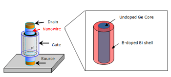
Schematic of a vertical transistor and an expanded view of its core-shell nanowire part. (AZONano.com)
Full story: here
No comments:
Post a Comment