


%20(1).png)
Here is A breakthrough news from IBM Watson Research Center on integrating CNTs down to 9nm contacts. This section from a recent interview with one of the researchers, Shu-Jen Han, behind this work taken from The IBM Research Blog:
Silicon has offered many advantages as a transistor material for the last half century. One biggest perhaps was that it forms a great gate dielectric – SiO2. It also comes with a very pure and high quality substrate, silicon wafers, to start with. And over time we’ve used other materials and device structures to improve its abilities, such as transitioning to high-k metal gate transistors and FinFETs.
On the other hand, for carbonnanotubes, many material issues have to be solved to obtain similar high-quality carbon nanotube wafers for device fabrication. We can’t switch to an entirely new material over night, but silicon is reaching its scaling limits.
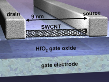
Dr. Qing Cao and my other teammates at [the IBM Watson Research Center] developed a way, at the atomic level, to weld - or bond – the metal molybdenum to the carbon nanotubes' ends, forming carbide. Previously, we could only place a metal directly on top of the entire nanotube. The resistance was too great to use the transistor once we reached about 20 nm. But welding the metal at the nanotubes' ends, or end-bonded contacts, is a unique feature for carbon nanotubes due to its 1-D structure, and reduced the resistance down to 9 nm contacts. Key to the breakthrough was shrinking the size of the contacts without increasing electrical resistance, which impedes performance. Until now, decreasing the size of device contacts caused a commensurate drop in performance.
For full details on this breakthrough research please see a recently published article in Science:
End-bonded contacts for carbon nanotube transistors with low, size-independent resistance
Qing Cao, Shu-Jen Han, Jerry Tersoff, Aaron D. Franklin, Yu Zhu, Zhen Zhang, George S. Tulevski, Jianshi Tang, Wilfried HaenschScience 2 October 2015:
Vol. 350 no. 6256 pp. 68-72
DOI: 10.1126/science.aac8006
Moving beyond the limits of silicon transistors requires both a
high-performance channel and high-quality electrical contacts.
Carbon nanotubes provide high-performance
channels below 10 nanometers, but as with silicon, the increase in
contact resistance
with decreasing size becomes a major performance
roadblock. We report a single-walled carbon nanotube (SWNT) transistor
technology
with an end-bonded contact scheme that leads to
size-independent contact resistance to overcome the scaling limits of
conventional
side-bonded or planar contact schemes. A
high-performance SWNT transistor was fabricated with a sub–10-nanometer
contact length,
showing a device resistance below 36 kilohms and
on-current above 15 microampere per tube. The p-type end-bonded
contact,
formed through the reaction of molybdenum with
the SWNT to form carbide, also exhibited no Schottky barrier. This
strategy
promises high-performance SWNT transistors,
enabling future ultimately scaled device technologies.
No comments:
Post a Comment