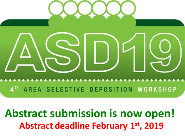
The 4th-annual Critical Materials Council (CMC) Conference will be held April 25-26, 2019 at the Saratoga Hotel and Casino in Saratoga Springs, New York. The public conference follows private CMC Fabs face-to-face meetings and Associate Members joint sessions April 23-24, at GlobalFoundries in Malta, New York.
Tuesday, February 5, 2019
Ultra-high on-chip optical gain in ALD erbium-based hybrid slot waveguides
Reliable on-chip optical amplifiers and light sources can enable integration of active functionalities on silicon based platforms.
Previously lasers integrated on silicon has been demonstrated with semiconductors by using methods such as wafer bonding or molecular beam epitaxy (MBE). These methods are however not that cost-effective in high volume manufacturing.
Now rearchers at Aalto University and Université Paris-Sud has now managed to significantly improve within chip data transmission using ALD Er:Al2O3 - a CMOS-compatible and scalable atomic-layer deposition process.
"The unique layer-by-layer nature of atomic-layer deposition enables atomic scale engineering of the gain layer properties and straightforward integration with silicon integrated waveguides. We demonstrate up to 20.1 ± 7.31 dB/cm and at least 52.4 ± 13.8 dB/cm net modal and material gain per unit length, respectively, the highest performance achieved from erbium-based planar waveguides integrated on silicon. Our results show significant advances towards efficient on-chip amplification, opening a route to large-scale integration of various active functionalities on silicon." [Nature Communications 2019, LINK]
Monday, February 4, 2019
Extended deadline for ASD 2019 Workshop
We are pleased to announce that the deadline for ASD abstract submission has been extended until Sunday 10 February. This means you have an extra ten days to finalize your abstracts and submit them at: abstract@asd2019-workshop.org
The workshop will feature the following invited speakers:
Rudy J. Wojtecki (IBM, USA), Katie Nardi (LAM Research, USA), Kanda Tapily (TEL, USA), Chi-I Lang (AMAT, USA), John Tolle (ASM, USA), Han-Bo-Ram Lee (Incheon National University), Gregory Parsons (NC State University, USA), Matthias Minjauw (University of Gent, Belgium), Necmi Biyikli (University of Connecticut, USA), Mohamed Saib (IMEC, Belgium), Efrain A. Sanchez (IMEC, Belgium), John G. Ekerdt (University of Texas, USA).
The workshop will cover a wide range of topics, including the following:
Area selective epitaxy and area selective chemical vapor deposition: processes and mechanisms, defects control
Intrinsic selectivity of ALD processes: nucleation and interface studies, chemical selectivity in surface reactions, competitive adsorption, precursors design, modeling of surface reactions
Methods for area selective activation / deactivation: use of inhibitors (self-assembled monolayers, polymers), plasma-/beam-induced activation
Processes and mechanisms for area selective atomic layer deposition: deposition of metals or dielectrics, thermal/plasma enhanced ALD, 3D or patterned substrates, substrates preparation, sequential deposition/etching,
Metrology and defects control: surface characterization techniques, selective etching of defects
Applications of area selective deposition: semiconductor industry (integration needs of device makers, solutions proposed by the equipment makers), catalysis, energy generation and storage, etc.
On behalf of the organizing committee, it will be our pleasure to welcome you in Leuven.
Andrea Illiberi Program Chair of the 4th ASD workshop
Sunday, February 3, 2019
Low temperature ALD of Rutheium using H2O as co-reactant
For those of you who were not surprised when Helsinki University published their Ru ALD processing using air as co-reactant please behold - Ruthenium ALD using H2O as co-reactant!
Self-catalyzed, Low-temperature Atomic Layer Deposition of Ruthenium Metal Using Zero-valent, Ru(DMBD)(CO)3 and Water
Zhengning Gao, Duy Le, Asim Khaniya, Charles L. Dezelah, Jacob Woodruff, Ravindra K. Kanjolia, William E Kaden, Talat S. Rahman, and Parag Banerjee
Chem. Mater., Just Accepted Manuscript
DOI: 10.1021/acs.chemmater.8b04456
Ruthenium (Ru) films are deposited using atomic layer deposition (ALD), promoted by a self-catalytic reaction mechanism. Using zero-valent, η4-2,3-dimethylbutadiene Ruthenium tricarbonyl (Ru(DMBD)(CO)3) and H2O, Ru films are deposited at the rate of 0.1 nm/cycle. The temperature for steady deposition lies between 160 ○C and 210 ○C. Film structure and composition is confirmed via x-ray diffraction, high-resolution transmission electron microscopy and x-ray photoelectron spectroscopy. The room temperature electrical resistivity of 10 nm Ru films is found to be 39 µΩ.cm. In situ quadrupole mass spectrometry and ab initio density functional theory are used to understand ALD surface reactions. The ligand, dimethylbutadiene dissociatively desorbs on the surface. On the other hand, the carbonyl ligand is catalyzed by the Ru center. This leads to the water gas shift reaction, forming CO2 and H2. Modulating deposition temperature affects these two ligand dissociation reactions. This in turn affects nucleation, growth and hence, Ru film properties. Self-catalyzed reactions provide a pathway for low temperature ALD with milder co-reactants.
Tuesday, January 29, 2019
An up-to-date and colorful ALD periodic table (to download)
Atomic Limits just published an overview of all materials prepared by atomic layer deposition (ALD) – An up-to-date and colorful periodic table (to download, LINK)
"As you might have noticed, we have just started a
year in which we celebrate the discovery of the Periodic System by
Dmitri Mendeleev: 2019 is the 150th anniversary of the
Periodic Table of Chemical Elements and has therefore been proclaimed
the “International Year of the Periodic Table of Chemical Elements (IYPT2019)” by the United Nations General Assembly and UNESCO."
The Importance of Atomic Layer Deposition (ALD) in Batteries
Here is a nice article on the importance of ALD in batteries by Dr. Arrelaine Dameron, Director of research and development at Forge Nano : "The Importance of Atomic Layer Deposition (ALD) in Batteries" [AZ Materials, LINK]
Forge Nano just recently recieved a USD 10 million invetsment by Volkswagen for new deveopment of ALD ofr lithium batteries [LINK].
Forge Nano ALD plant for coating tons of battery material required by the automobile industry (Picture: ForgeNano/AZ Materials)
Monday, January 28, 2019
Entegris and Versum Materials to Combine in $9 Billion Merger of Equals to Create A Premier Specialty Materials Company
BILLERICA, Mass. & TEMPE, Ariz.--(BUSINESS WIRE)--Entegris, Inc. (NASDAQ:ENTG), a leader in specialty chemicals and advanced materials solutions for the microelectronics industry, and Versum Materials, Inc. (NYSE:VSM), a leading specialty materials supplier to the semiconductor industry, today announced that they have agreed to combine in a merger of equals. The combined company will be a premier specialty materials company for the semiconductor and other high-tech industries.
Under the terms of the agreement, which was unanimously approved by the Boards of Directors of both companies, Versum Materials stockholders will receive 1.120 shares of Entegris for each existing Versum Materials share. Upon completion of the merger, Entegris stockholders will own 52.5 percent and Versum Materials stockholders will own 47.5 percent of the combined company1. The combined company will have a pro forma enterprise value of approximately $9 billion, based on the closing prices of Entegris and Versum Materials on January 25, 2019, and approximately $3 billion in revenue and approximately $1 billion in Adjusted EBITDA on a pro forma basis for calendar year 20182.
The combined company will retain the Entegris name and will be headquartered in Billerica, Massachusetts, and will maintain a strong operational presence in Tempe, Arizona.
Upon closing of the transaction, Entegris CEO Bertrand Loy will serve as Chief Executive Officer, Entegris CFO Greg Graves will serve as Chief Financial Officer, and Versum Materials General Counsel Michael Valente will serve as General Counsel of the combined company, supported by a highly experienced and proven leadership team that reflects the strengths and capabilities of both companies.
The combined company’s Board of Directors will have nine members, consisting of four directors from the existing Versum Materials board, including Seifi Ghasemi, Chairman of the Versum Materials Board, who will serve as Chairman of the Board of the combined company, and five directors from the existing Entegris Board, including Bertrand Loy.
Entegris President and Chief Executive Officer, Bertrand Loy said, “We are excited to combine with Versum Materials to create a premier specialty materials company for the semiconductor and other high-tech industries. The combined company will be ideally positioned to more effectively help our customers achieve higher yields and new levels of performance and reliability, and together, we will be well positioned to take advantage of long-term secular semiconductor growth, and to tackle new industry process challenges. I have great respect for the Versum Materials team and look forward to joining forces as we embark on this next chapter and create new value for our stockholders, employees and customers.”
Versum Materials President and Chief Executive Officer, Guillermo Novo said, “We could not ask for a better partner in Entegris. This merger will create greater benefits and growth opportunities than either company could have achieved on its own. It dramatically accelerates our goal of portfolio diversification – creating an end-to-end materials solutions provider across the entire semiconductor manufacturing process. With enhanced global scale and world class technical expertise, we’ll be poised to drive further innovation and support investments across our technology, infrastructure, and additional capabilities – enabling us both to better serve our customers and provide expanded opportunities for our employees.”
Compelling Strategic and Financial Benefits of the Merger
Enhanced product breadth and depth: Entegris and Versum Materials have highly complementary portfolios that combined will bring customers enhanced technical capabilities. This merger will create the world’s first comprehensive and effective end-to-end materials solutions provider across the entire semiconductor manufacturing process. The combined company is expected to have a full suite of diversified product offerings including Advanced Materials, Specialty Gases, Microcontamination Control, Advanced Materials Handling, and Delivery Systems and Services.World class technology: The combined company’s world class technology and R&D capabilities will better enable it to:
- Address customers’ evolving needs for new materials as device architectures become more complex;
- Capitalize on the increasing demand for purity and help drive improved yield; and
- Accelerate the development and time to market of new technologies that align with the industry technology roadmap.
- Global scale and operational excellence: A much broader, global scale will enable the combined company to reach additional customer touch points, and have increased relevance in key geographies. By combining its extensive global manufacturing network, the company will be able to improve delivery times and drive new levels of operational efficiencies and excellence.
- Increased financial strength and flexibility: The combined company will have approximately $3 billion in revenue and approximately $1 billion in Adjusted EBITDA on a pro forma basis for calendar year 20183. It will be well capitalized with a strong balance sheet and a pro forma net leverage ratio of 1.1x4. In addition, it will have flexibility to invest, make acquisitions, and return capital to stockholders, while enjoying greater earnings stability and margin growth potential.
- Significant stockholder value creation: The combination is expected to generate more than $75 million of annual cost synergies in manufacturing, logistics, procurement and SG&A rationalization within 12 months post close. In addition, the combined company is expected to realize significant revenue growth synergies from cross-selling opportunities, with further potential upside from capex and revenue synergies.
Saturday, January 26, 2019
Oxford Instruments Partners ITRI for Micro LED Development with Plasma Etch Solutions
[LED Inside, LINK]
Oxford Instruments Plasma Technology (OIPT) announced that it has
worked with Taiwan’s Industrial Technology Research Institute (ITRI) by
providing multiple PlasmaPro 100 systems including both etch and
deposition for ITRI’s Micro LED R&D program.
The
PlasmaPro 100 ICP process solutions are designed to support leading
edge device applications such as Lasers, RF, Power and advanced LEDs.
Thursday, January 24, 2019
Volkswagen invests USD 10 M in US ALD start-up Forge Nano for battery material research
The Volkswagen Group is investing US$10 million in the start-up Forge Nano Inc with a view to reinforcing its specialist knowledge in the field of battery research. Forge Nano is investigating a material coating technology that could further improve the performance of battery materials. As a partner, Volkswagen will provide support for industrial trials of this technology. The transaction is still subject to approval by the authorities.
(forgenano.com)
Volkswagen has been collaborating with Forge Nano on advanced battery material research since 2014. The startup with headquarters in Louisville, Colorado, is investigating processes for scaling atomic layer deposition (ALD) to create new core-shell materials, especially for battery applications. ALD is a chemical process for applying atomic scale coatings one atom at a time. With its specific ALD technology, Forge Nano aims to boost energy density of vehicle battery cells.
For example, a higher energy density would have positive effects on the range of electric vehicles. Volkswagen has been lending their automotive and battery expertise towards Forge Nano’s applied research efforts.
The Volkswagen Group is consistently forging ahead with its electric offensive and intends to offer more than 50 battery-electric models by 2025, accounting for about a fifth of its entire model portfolio. To safeguard this approach, Volkswagen is cooperating with strategic battery cell suppliers and developing its own specialist know-how in battery research. This also includes targeted venture investments. Volkswagen is increasingly investing in international start-ups to bring innovative technologies forward to production maturity together.
Dr. Axel Heinrich, Head of Volkswagen Group Research, said: “At Volkswagen, we want to be the world’s leading provider of e-mobility. We are continually expanding the battery technology know-how required for this purpose. We need to safeguard our technological competence for the future. Cooperation with start-ups is a key element in these efforts. We are acting as a partner to Forge Nano and intend to provide the team with opportunities to carry out industrial trials with its innovative technology.”
Dr. Paul Lichty, Founder and CEO of Forge Nano, said: “Our atomically precise surface engineering technology is ushering in a new era of high performance materials. We are excited to partner with a company that has such a strong commitment to commercializing innovation.”
Wednesday, January 23, 2019
ASM International enhances ALD productivity with new 300 mm XP8 Quad Chamber Module
ASM International enhances ALD productivity with new very competetive 300 mm XP8 Quad Chamber Module providing:
- High productivity platform for PEALD and PECVD Processing of up to 16 wafers at a time.
- Integrated processing using both the "old" Double (DCM) and new Quad Chamber Modules (QCM) for flexibility and productivity optimization.
- Earlier in 2018 ASM relaunched the two industry ALD workhorse chambers, Pulsar Thermal ALD and Emerald PEALD used for e.g. HKMG, as Double module on XP8 - this now means that all ASM ALD and PEALD chambers can be used on the high productivity platfrom XP8 eilter sa DCM or QCM or both.
Quad chamber modules (QCMs) 30, 32, 34, and 36 are connected to four side surfaces of the vacuum chamber 22. Each QCM is a module having four reactor chambers (RC1 to RC4). Processing such as plasma film forming processing is performed on a substrate in each reactor chamber. (ASM Patent application US20170278074A1)
"Across the board, customers are requiring increased throughput" said Tominori Yoshida, ASM's General Manager and Senior Vice President, Plasma Products Business Unit. "The XP8 QCM addresses advanced PEALD and PECVD films including silicon oxide for multiple patterning and silicon nitride for other applications, and relatively thick films where the tool's architecture enables higher throughput compared to other single-wafer configurations."
The new reactor architecture is well-suited for high-volume advanced-node memory and logic applications, which require the precise film control provided by the QCM's innovative reaction chamber. The QCM chambers use the same advanced reactor technology as ASM's original PEALD and PECVD XP8 Dual Chamber Modules (DCMs). Hundreds of these DCMs have been running for years in high-volume production globally at key logic, foundry and memory customers. This allows customers to easily transfer existing processes to the new QCM chamber. As a result, the XP8 QCM tool is already in high-volume manufacturing at multiple customers worldwide.
Furthermore, the XP8 architecture enables integrated processing using both DCMs and QCMs for flexibility and productivity optimization.
Strem Chemicals’ offers new La-FMD ALD precursor for future leading edge logic and memory products
Strem Chemicals’ offering of La-FMD is one of the most promising metal-amidinate ALD precursors for lanthanum (La) based ALD thin-films which are potentially strong candidates for high-k gate dielectric in the next generation of CMOS technology.
Rare earth elements have entered high volume manufacturing for advanced logic devices since the 32 nm node (IBM, Samsung and Globalfoundries – Chipworks 2010). Especially for Lanthanum (La) — the eponym of the lanthanide series in the periodic table has been implemented as a dopant in the high-k metal gate stack. Lanthanum oxide (La2O3, dielectric constant ~ 27), for example, has been explored for two decades as a high-k gate dielectric for the replacement of conventional silicon dioxide (SiO2) gate dielectric in the next generation transistors in logic as well as in dynamic random access memories (DRAMs).
Keyword
segmentation of patent applications the last 20 years for Lanthanum and “Atomic
Layer Deposition” [Patbase search 15 November 2018]
Atomic layer deposition is the most promising method for growing ultra-thin-films of La based gate dielectrics and has therefore been under extensive research and filing of patent applications in the last 20 years. The R&D effort has been focused on fields relating to dielectric and high-k dielectric applications in the semiconductor industry (see keyword segmentation above). The atomic layer-by-layer film growth facilitated by self-limiting surface reactions in ALD provides atomically precise film-thickness control, good uniformity across a large area substrate, and excellent conformality in case of high aspect ratio structures like modern FinFETs and memory capacitor type pillar structures. However, to work flawlessly it requires the ALD precursors that have specific properties (LINK):
1. Sufficiently volatile (at least ~ 0.1 Torr equilibrium vapor pressure at a temperature at which they do not decompose thermally).
2. Rapidly vaporizing and at a reproducible rate (conditions that are usually met for liquid precursors, but not for solids).
3. Not self-reacting or decomposing on the surface or in the gas phase (for self-terminating surface reactions).
4. Highly reactive with the other reactant previously attached to the surface, which results in relatively fast kinetics and thus lower ALD temperatures and cycle times.
5. Volatile byproducts that can be easily purged in order to prepare for the subsequent half-cycle.
6. Non-corrosive byproducts to prevent non-uniformities due to film etching and corrosion of the tool.
In 2007, Intel Corporation
incorporated HfO2 into high-k gate dielectric stack at 45 nm technology
node. However, pure HfO2 suffers from low-k interface layer problem
with Si, limiting lower equivalent oxide thickness (EOT) values. It also
readily crystallizes at temperatures as low as ~500°C. Therefore,
amorphous dielectrics with high thermal stability are still sought after
for no intrinsic defects (e.g. grain boundaries), provided they still
offer the advantages of HfO2, such as high dielectric constant, wide
band-gap, and low leakage current. Lanthanum-based ternary oxides,
such as lanthanum scandate (LaScO3) and lanthanum lutetium oxide
(LaLuO3), deposited by ALD process involving metal amidinate precursors
reportedly exhibit desirable structural and electrical properties. In
fact LaLuO3
is potentially the best amorphous phase gate dielectric with dielectric
constant k~32. It doesn’t form low-k interfacial layers with Si which
enables effective oxide thickness (EOT) values < 1 nm with
significantly low leakage current. Another factor contributing to the
low leakage current across ALD grown thin LaLuO3 gate dielectric is the
large band-offset (2.1 eV) with respect to Si; the symmetric conduction
and valence band offsets result into equal leakage currents in electron
driven NMOSFETs and hole driven PMOSFETs. It stays amorphous and doesn’t
form alloys with Si or Ge after respective source/drain activation
anneals.
As a very recent example of an actual high aspect ratio application on 300 mm wafers requiring all ALD precursor characteristics described above (1 to 6) we can see the paper that Imec presented at this famous IEDM conference, on using a LaSiOx layer as a dipole inserted in the HKMG stack. Imec succeeded in stacking the complete FinFET front end module on top of a "standard" bulk silicon FinFET module demonstrating also good threshold voltage tuning, reliability and low-temperature performance. Presumably it has most likely been deposited by an ALD process since it will have to conformally coat the fins and ensure precise thickness control and uniformity : IEDM2018 Paper #7.1, “First Demonstration of 3D Stacked FinFETs at a 45nm Fin Pitch and 110nm Gate Pitch Technology on 300mm Wafers,” A. Vandooren et al, Imec [LINK].
As in this case and many more, the stringent
qualifications for ALD precursors put them in the category of high quality
specialty chemicals — the performance or function specific materials or
molecules of choice. The deposited film properties are strongly influenced by
the physical and chemical properties of a single molecule or a formulated
mixture of molecules as well as its chemical composition. Therefore, it puts a
lot of pressure on the manufacturer and supplier of the high purity specialty
chemicals in terms of quality, purity, documentation procedures, customer
service etc.
Friday, January 18, 2019
ULVAC Inc. and Oxford Instruments Plasma Technology collaborate to bring Atomic Scale Processing solutions to the Japanese Power and RF markets
[Oxford Instruments, LINK] Leading semiconductor equipment solution providers, Oxford Instruments Plasma Technology (a trading name of Oxford Instruments Nanotechnology Tools Limited, Tubney, Oxford, UK) and ULVAC Inc., (Chigasaki, Kanagawa, Japan) are delighted to announce a key collaboration which will bring leading edge deposition and etch technology solutions to GaN and SiC based Wide Band Gap production customers in Japan.
“Oxford Instruments Plasma Technology is excited to be collaborating with ULVAC in order to bring its proven process solutions to the Japanese power and RF markets”, commented Mike Gansser-Potts, Managing Director, Oxford Instruments Plasma Technology. “This relationship, which will begin with ULVAC as our channel partner in Japan, will allow local production customers access to Oxford Instruments’ suite of Atomic Scale Processing solutions”
“This is indeed a very significant collaboration”, confirmed Tetsuya Shimada, General Manager for Advanced Electronics Equipment Division of ULVAC Inc., “Our new collaborator, Oxford Instruments Plasma Technology, has critical process technology and know-how which complements our own capabilities. Combined with our customer support infrastructure this will allow us to provide a complete solution to our Japanese customers.”
Oxford Instruments Plasma Technology’s Atomic Layer Deposition (ALD) and Atomic Layer Etch (ALE) are critical process steps for GaN and SiC based devices to enable functionality and reliable device manufacturing. With the critical know-how and expertise gained over the last ten years in Wide Band Gap applications, Oxford Instruments Plasma Technology is perfectly placed to serve the technology leading Japanese production customers in these markets.
Wednesday, January 16, 2019
Come to Berlin for the EFDS ALD for Industry - 3rd Workshop and Tutorial, March 19-20, 2019
Including Industrial Exhibition and Practical ALD Show
A topical workshop with focus on industrialization and commercialization of ALD for current and emerging market
Atomic
Layer Deposition (ALD) is used to deposit ultraconformal thin films
with sub-nm film thickness control. The method is unique in the sense
that it employs sequential self-limiting surface reactions for growth in
the monolayer thickness regime. Today, ALD is a key technology in
leading semiconductor technology and the field of application in other
leading-edge industries is increasing rapidly. According to market
estimates the equipment market alone is currently at an annual revenue
of US$ 1.5-1.7 billion (2017) and it is expected to double in the next
4-5 years.
In a European context ALD was invented independently twice in Europe (Russia & Finland) and since the last 15 years Germany has grown to become one of the strongest European markets for ALD in R&D, chemicals, equipment and end users.
The Event will focus on the current markets for ALD and addresses the applications in semiconductor industry, MEMS & Sensors, Battery Technology, Medical, Display, Lightning, Barriers and Photovoltaics.
Location: Fraunhofer-Forum Berlin
Tuesday, January 15, 2019
CALL FOR PAPERS - 4th Area Selective Deposition (ASD) Workshop will be held on April 4th – 5th, 2019 in IMEC, Leuven (Belgium)
Visit
our website:
ASM and IMEC are
proud to announce that the 4th Area Selective Deposition (ASD)
Workshop will be held on April 4th – 5th, 2019 in IMEC,
Leuven (Belgium).
This workshop will
bring together leading experts from both academia and industry to share their
vision and results on ASD. Based on a series of successful workshops at the:
North Carolina State University in 2018, Eindhoven University of Technology in
2017 and IMEC in 2016, the two-days program will include invited and
contributed speakers, a poster session and a reception on the evening of April
4th.
Area selective epitaxy and area selective chemical vapor deposition: processes and mechanisms, defects control
Intrinsic selectivity of ALD processes: nucleation and interface studies, chemical selectivity in surface reactions, competitive adsorption, precursors design, modeling of surface reactions
Methods for area selective activation / deactivation: use of inhibitors (self-assembled monolayers, polymers), plasma-/beam-induced activation
Processes and mechanisms for area selective atomic layer deposition: deposition of metals or dielectrics, thermal/plasma enhanced ALD, 3D or patterned substrates, substrates preparation, sequential deposition/etching,
Metrology and defects control: surface characterization techniques, selective etching of defects
Applications of area selective deposition: semiconductor industry (integration needs of device makers, solutions proposed by the equipment makers), catalysis, energy generation and storage, etc.
On behalf of the organizing committee, it will be our pleasure to welcome you in Leuven.
Andrea Illiberi
Program chair of the 4th ASD workshop
Thursday, January 10, 2019
Workshop, Tutorial & Practical Show „ALD for Industry“, 19. – 20. März 2019, Berlin
ALD – eine vielversprechende Technologie
Die Atomlagenabscheidung (ALD) verspricht mit ihrem besonderen Ansatz, Beschichtungen Lage für Lage geordnet abzuscheiden, zahlreiche Vorteile und Möglichkeiten. 2019 treffen wir uns nunmehr zum dritten Mal mit zunehmendem Teilnehmerkreis, um das Potential der Technologie und die aktuellen Fortschritte aufzuzeigen und zu diskutieren. In diesem Jahr stehen neben interessanten Vorträgen vor allem Praxistipps im Vordergrund. In der „Practical ALD Show“ geben Experten Tipps zur Durchführung und Prozessoptimierung. Einzelne Ausstellungs-Restplätze für Sponsoren sind noch buchbar.
Das Jahrestreffen der Plasma- und Vakuumexperten – V2019 + ALD
Das Jahrestreffen der Plasma- und Vakuumexperten – V2019
+ ALD (Vorlesung, Poster, Workshop)
Die Vorbereitungen laufen auf Hochtouren. Die V2019 wird in diesem Jahr wieder zahlreiche Experten, Anbieter, Nachwuchskräfte und Interessierte zur Vakuum- und Plasmaoberflächentechnik zusammenführen. Diesmal findet das Event in der Saalebene des Internationalen Congress Center Dresden (ICD) statt – welches gleich an die historischen, barocken Bauwerke der Altstadt anschließt. Die diesjährige V verbindet Bewährtes und Neues. Da sind neben Vorträgen und Fachgesprächen die zahlreichen Industrieaussteller aber auch neue Workshop-Themen, ein Fachkräfte-Scouting und Firmenbesichtigungen zu erleben. Seien Sie beim Branchentreff dabei. Zahlreiche Aussteller haben bereits Ihren Stand gebucht.
Sichern Sie sich rechtzeitig Ihre repräsentative Ausstellungsfläche.
Subscribe to:
Posts (Atom)