Tuesday, April 24, 2018

RASIRC to Present Anhydrous Hydrogen Peroxide Surface Preparation and Enhanced Nucleation for ASD at ASD2018

Area selective deposition is becoming increasingly important for the immense scaling effort continuously taking place in the semiconductor industry for Logic and Memory Devices. Today double and multiple pattering schemes using Plasma Enhanced ALD are in High Volume Manufacturing (HVM) for all sub 28 nm nodes and any moment now the industry expect to ramp EUV lithography, possibly at the 7 nm Foundry Node. Beyond that in a joint effort the researchers and the industry are looking for alternative patterning methods and many of them are based on so called bottom-up patterning.

To put things in perspective for ASD, one of the first area selective ALD processes in HVM was introduced in 300 mm DRAM manufacturing by Infineon Technologies in 2004 (90 nm Deep Trench DRAM presented in detail at IEDM 2004). This area selective ALD process relied on controlling the amount of hydroxyl groups in the upper part of a trench structure using the well-known TMA / H2O based process growing Al2O3. The goal was to let the process partially penetrate about 1 micron deep into very deep DRAM trenches to protect the silicon surface from a following isotropic etch that would widen the deep trench creating more surface and therefore allow a higher capacitance of the memory cell which is a key performance parameter in DRAM at about 25 fF/cell at that time.

In addition, the liner protected the collar region from dopant penetration keeping a well-defined dopant profile isolated from the wafer surface where the select transistor would later operate and it also defined a selective area for growth of Hemi-Spherical Grains (HSGs) another surface area expansion technology used in the DRAM industry. Please check the patent visualized below for many more details. This fascinating process was Self-Aligned and Area Selective in so many ways and kicked out a number of complex alternative integration paths saving a lot of $/wafer. By optimizing all process parameters it was possible to control the penetration depth of the liner, the transition region length down to the non-growth area, wafer uniformity and liner quality (density). This process was used until the end of the Deep Trench era which at this time had ~25% of the DRAM market but was killed at 65 nm when all companies had transitioned to stacked memory cells.

The Non-conformal ALD Al2O3 liner application as described in the US patent “Process for vertically patterning substrates in semiconductor process technology by means of inconformal deposition” (Figure from US7344953B2) 


Since then several things have happened. For one thing ALD has become a standard processing technology in Logic and Memory HVM forming its own Business Segment with an annual Equipment revenue >USD 1.5 Billion. Secondly, Atomic Layer Etching (ALE) has also entered HVM at the Logic 14 nm FinFET manufacturing. In parallel several efforts have begun to explore novel methods for ASD. These utilize Self-Assembled Monolayers, Patterned Photoresists, Selective CVD processes (e.g. Cobalt CVD), Plasma deposited films and other creative surface blocking agents and employing ALD and ALE in combination to trigger or block surface growth.  In parallel, reactive surfaces must be created for high nucleation and growth of metal oxide films.  An ideal surface treatment for the latter will:

                  Create high density surface functionalization
                  Have zero or minimal sub-surface oxidation
                  Lead to faster and more uniform nucleation versus H2O
                  Remain non-reactive with organic functionality or photoresist on adjacent surfaces

The use of the novel reactive chemistry, anhydrous hydrogen peroxide, has been largely ignored. This is due to: a lack of literature precedent; that H2O2 is typically delivered with H2O (multiple publications from K. Kukli et al at University of Helsinki and Tartu) where water dominates the reaction chemistry; and that only recently did this material become available by RASIRC (San Diego, USA) in an ampoule form that could be integrated into ASD process equipment.

Besides water, Ozone is an important co-reactant and oxidative precursor in ALD of metal oxides for, e.g., High-k dielectrics in DRAM Capacitors. Hydrogen Peroxide has similar oxidation properties to Ozone (oxidation potential O3 = 2.1V versus 1.8V for H2O2) while simultaneously having slightly stronger proton transfer properties than water (water pKa = 7.0 versus 6.5 for H2O2). According to Jeff Spiegelman (CEO and Founder of RASIRC) the key learning from early discoveries is the fact that H2O2 has a very weak O-O bond, where Bond Energy = 36 kcal/mole and you can imagine that it is thus much more readily available to conduct reactive surface chemistry in an ALD process than the oxygen atom in the water molecule.

RASIRC and their collaborative network of leading scientists and customers around the world have in recent years conducted exciting work with anhydrous hydrogen peroxide that demonstrates the following with regard to the required attributes for ASD:

                  Dry H2O2 creates 3-5 times higher nucleation surface density of hydroxyl groups
(-OH) versus water on metal surfaces
                  Monolayer hydroxyl (-OH) surface functionalization can be obtained by dry H2O2 on Si surfaces without sub-surface oxidation
                  Faster nucleation and growth of Al2O3  is observed utilizing dry H2O2 on Si-H surfaces versus H2O
Little to no Photoresist removal occurs from reaction with hydrogen peroxide at temperatures up to 300°C.

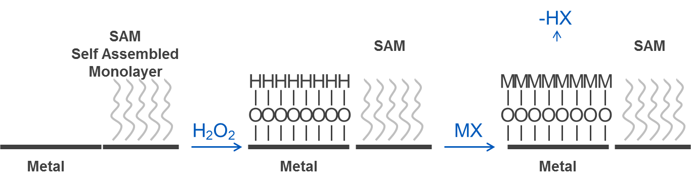
BRUTE Peroxide Ideal Chemistry for Area Selective Deposition yielding: High density surface hydroxylation, minimal sub-surface oxidation, faster and more uniform nucleation versus H2O, non-reactive with protecting groups on adjacent surfaces and Peroxide will grow a High Quality Metal Oxide
 

In addition, RASIRC has demonstrated that metal oxide films such as the most important ones; Aluminum oxide, Hafnium oxide, and Zirconium oxide have high quality film properties nearly identical to those grown by ozone methods.


In 3D-structures with extreme high aspect ratio (DRAM, 3DNAND) ozone will penetrate deep down the structure before reacting with the surface groups since the sticking coefficient is much smaller than H2O or preferably H2O2. This means that area selectivity employing ozone is difficult to achieve. You can imagine that Dry H2O2 would have been very beneficial back in 2004 for the non-conformal liner case described above by allowing use of a much thinner liner with higher density and therefore higher thru-put. Potentially also Dry H2O2 would allow for a sharper transition region – to be discovered!

RASIRC Chief Technology Officer Dan Alvarez will present additional details on the newly discovered reactivity of anhydrous hydrogen peroxide on several surfaces as well as outline some potential ASD pathways at AVS ASD2018, North Carolina State University, April 29 to May 1, 2018. (https://asd2018.avs.org/)

This is the 3rd time the ASD Workshop will be held. It is a fully supported AVS event and there has been a growing interest in ASD. In the future we can expect that it will form a solid business segment as ALD and ALE and bring in new players, both academic and industrial, in the exciting field of Atomic Level Processing!


Groundbreaking micromedicine with Picosun’s ALD solutions

ESPOO, Finland, 24th April, 2018 – Picosun Group, a leading industrial supplier of Atomic Layer Deposition (ALD) thin film coating technology, reports of groundbreaking results in ALD biobarriers for novel medical applications.

Picosun’s ALD biobarriers are developed specifically for hermetic encapsulation and passivation of critical electronics in implantable micromedical devices for e.g. cardiological and neurological treatments. The purpose of the biocompatible ALD barrier layers is to protect the microelectronic components of the devices without interfering with the device functionality. The results are excellent: Devices with the ALD biobarriers lasted for several months in accelerated aging tests, equaling at least ten years inside a human body, whereas non-protected devices started to deteriorate already in a matter of hours. (*)
Picosun’s ALD biobarriers are developed specifically for hermetic encapsulation and passivation of critical medical tools and electronics in implantable micromedical devices for e.g. cardiological and neurological treatments (left and center). Newly appointed CTO of Picosun Group, Dr. Jani Kivioja, (right), previously at NOKIA Digital Health lab (Espoo, Finland) and NOKIA Nanomaterials (Cambridge, UK).
Medical technology is one of the key industries that reaps the benefits of the on-going digitalization and miniaturization of electronics. Instead of heavy surgeries and clumsy, expensive machines that require frequent hospital visits of the patients, diagnostics and treatments can be performed remotely and with minimally invasive methods utilizing various minuscule devices that can be either implanted inside the body or attached to skin. Lab-on-a-chip devices which combine microfluidics and microelectronics allow fast and cost-efficient in-situ analysis of body fluid and tissue samples. Implantable sensors can monitor blood glucose, blood pressure, intraocular and intracranial pressure, and heart functions. Parkinson’s and potentially many other brain diseases can be treated with implanted probes that provide electrical stimulation to the critical regions of the brain. In cardiology, catheter ablation, the common treatment of cardiac arrhythmias, can be made safer and more precise with the help of state-of-the-art microelectronics and sensor technology. Especially the elderly population benefits from these solutions when remote monitoring of various physiological markers allows them to live longer at home and severe conditions can be detected before they require long and costly hospital treatments.

Saturday, April 21, 2018

ASM International N.V. Reports First Quarter 2018 Results

ASM International N.V. (Euronext Amsterdam: ASM) reports its first quarter 2018 operating results (unaudited) in accordance with IFRS. (Almere, The Netherland April 19, 2018 FinanzNachrichten.de LINK)

From the ASMI Q1/2018 investor presentations : LINK
  • New orders at €206 million were at the highest level ever and 2% above the Q4 2017 level and 1% above the level of Q1 2017.
  • Net sales for the first quarter 2018 were €159 million, a decrease of 12% compared to the restated previous quarter.
  • Gross profit margin was 37.8% in Q1 2018. The margin was beside the effects of new product introductions impacted by sales mix and preparation for anticipated higher activity levels.
  • Operating result decreased to €12 million compared to the previous quarter. The decrease is mainly the result of the lower sales level.
  • Normalized net earnings for the first quarter 2018 decreased by €18 million compared to the fourth quarter 2017.

Versum Materials Celebrates the Grand Opening of Its R&D Facility in Hometown, PA

TEMPE, Ariz. (April 19, 2018) Versum Materials, Inc. (NYSE: VSM), a leading materials supplier to the semiconductor industry, announced today the grand opening of its new research and development (R&D) facility at its semiconductor materials manufacturing site in Hometown, Pennsylvania. The ribbon-cutting ceremony took place April 10, 2018. Versum employees, members of the community, local government, customers and strategic partners attended the event.

The state-of-the-art R&D laboratory is dedicated to new materials used in the manufacture of semiconductors. Scientists in the facility will synthesize and purify new molecules down to parts per billion impurity levels and below using the latest technologies available in the industry. The researchers can assess the applications for these new molecules and scale up the molecules to larger quantities for customer evaluation. These new organometallic compounds will be deposited on semiconductor wafers through cutting-edge technologies to test their performance for semiconductor applications. Additionally, the facility is capable of small-volume manufacturing and advanced analytical and quality assessment.
 
 
State Senator Dave Argall commended Versum for being the region’s third largest employer and for the company’s investments in the local community. Approximately 30 employees, half of which hold advanced degrees in chemistry or chemical engineering, are based in the new facility. The company’s Hometown campus now totals 250 highly-skilled employees.

Thursday, April 19, 2018

Curious2018 - Merck 350th Anniversary Scientific Flagship Conference & Research Grant July 16th-18th

On the occasion of its 350th anniversary Merck is initiating the scientific flagship conference, the Curious2018 – Future Insight Conference on July 16th-18th in Darmstadt, Germany. The conference brings together some of the greatest scientists, including five Nobel laureates, and most accomplished entrepreneurs of the world to discuss the future of science and technology. 
 
For a list of speakers see: https://curious2018.com/speakers/

You or anyone in your network are cordially invited to apply for a free ticket, deadline May 1st, 2018, at: https://curious2018.com/attend/application-tickets/
 

350 Research Grants:

Finally, In celebrating its 350th anniversary, Merck offers a series of research grants to stimulate innovative research in challenging areas of future importance. Merck intends to provide several research grants of up to EUR 350,000 per year for 3 years in various the areas of Drug Discovery, Synthetic Biology, Materials and Solutions, and Digitalization with the option of extension or expansion. 


Monday, April 16, 2018

NCD Contracted with TIANMA to supply 6G half ALD equipment for flexible OLED encapsulation

NCD recently signed a contract with TIANMA, one of Chinese leading display manufacturers, to provide 6G half ALD equipment for encapsulation of flexible OLEDs in the next six months to Wuhan TIANMA. This is a follow-up order to purchase NCD's 6G half (1500mmX925mm) ALD equipment, which is based on the superior performance evaluation of earlier installed 5.5G class ALD equipment in Shanghai TIANMA.

The performance of ALD encapsulation by the existing equipment showed excellent film uniformity as well as excellent moisture permeability and step coverage, compared to that by PECVD, and was qualified by the customer's flexible OLED products.

This proves that NCD's ALD core technology and the reliability of equipment have been recognized by its customer.
 
It is challenging to realize device reliability using current encapsulation technology deposited by PECVD for the next generation flexible OLED devices, since it requires bending, folding and rolling, ALD technology will be an essential choice for future flexible OLED products with its excellence and competitiveness.

NCD will make the Lucida GD series become the standard ALD equipment for all flexible OLED encapsulation based on these needs, and continue to grow into the world's most professional ALD Company with new challenges and developments. 
 
 
Cluster system for Lucida™ GD series

Saturday, April 14, 2018

The Material Discovery Funnel: A Six-Step Process for Advanced Material Development

The forward march of technology relies on continuous improvement of critical components such as semiconductors, batteries, fuel cells, and the like. In time, every component runs up against performance constraints established by fundamental physics and chemistry. Overcoming those restrictions requires the development of unique advanced materials that circumvent such limitations. Discovering and optimizing these types of new materials is difficult because the range of variables creates an enormous design space that is difficult to explore efficiently. Combinatorial deposition refers to a process of creating many advanced material candidates on a single substrate without removing that substrate from the chamber during the deposition process. The technique is not new in concept, but the remarkable advancements in deposition chamber capabilities and controls are making combinatorial deposition easier to implement. We refer to the process of developing advanced materials using combinatorial deposition as the "material discovery funnel."
 
The material discovery funnel - PVD Products
 
As described by PVD Products this is a six step process. You can visit their Blog and get the download link to the excellent white paper!

Source: PVD Products Blog LINK

Thursday, April 12, 2018

Biologically inspired ALD:ed nanomembrane purges coal-fired smoke of greenhouse gases

(Nanowerk News) A biologically inspired membrane intended to cleanse carbon dioxide almost completely from the smoke of coal-fired power plants has been developed by scientists at Sandia National Laboratories and the University of New Mexico. The patented work, reported recently in Nature Communications ("Ultra-thin enzymatic liquid membrane for CO22 separation and capture"), has interested power and energy companies that would like to significantly and inexpensively reduce emissions of carbon dioxide, one of the most widespread greenhouse gases, and explore other possible uses of the invention. 


Enzymatic liquid membrane design and mechanism of CO2 capture and separation. a The membrane is fabricated by formation of ~1-µm-deep oriented arrays of 8 nm diameter cylindrical silica [SiO2] mesopores within the larger 50–150-nm pore channels of a 50-μm-thick porous alumina [Al2O3] Whatman© Anodisc support. b Using atomic layer deposition and oxygen plasma processing (described in text and Fig. 4) the silica mesopores are engineered to be hydrophobic (trimethylsilyl (Si(CH3)3) surface groups) except for an 18-nm-deep region at the pore surface, which is hydrophilic (≡Si-OH surface groups). Via capillary condensation, CA enzymes and water spontaneously fill the hydrophilic mesopores to form an array of nano-stabilized CA enzymes with an effective CA concentration >10× of that achievable in solution. CA catalyzes the capture and dissolution of CO2 as carbonic acid (HCO3) moieties at the upstream surface and regeneration of CO2 at the downstream surface (see Fig. 1c). The high concentration of CA and short diffusion path length maximizes capture efficiency and flux (Nature Communications article LINK)

Full article: LINK

Beneq C2 wins the High-Volume Manufacturing Award in the CS International Conference

 
Beneq C2 wins the High-Volume Manufacturing Award in the CS International Conference. Beneq C2, the automated wafer ALD solution in Beneq’s cluster-compatible equipment portfolio, is the winner in the High-Volume Manufacturing category of the CS Industry Awards, where the industry experts have been able to vote for their favorites. 
 
Dr Mikko Söderlund receives CS Industry Award for Beneq

Beneq's Mikko Söderlund with the High-Volume Manufacturing Award in the CS Award ceremony.
 
Source : Beneq Blog

Tuning PEALD film propperties by substrate biasing for planar and 3D applications

After having worked with dry etch people etching deep into silicon and advanced HKMG stack and other challenging and amazing things like longitudinal splitting of nanowires my experience is that they have a totally different level of insight to plasma processing technology than me the typical ALD guy. Substrate biasing is such a technology that we the usual suspects in ALD have limited insights to. You can almost hear how they laugh at us loud when we turn on our funky PEALD chambers and let the wafer float in an undefined potential state - it´s like taking a shower up in the international space station without any special precautions.

The TU Eindhoven Plasma Pro´s and their friends from Oxford Instruments, prove it time after time buy pushing out these great publications explaining to us who thinks plasmas are some sort of voodoo, They show us how it all really works in PEALD. Here is one of the most recent ones and next (April 19th) you may tune in to the Oxford Instruments Webinar and listen to Harm Knoops telling us how it really works (LINK).

Tuning Material Properties of Oxides and Nitrides by Substrate Biasing during Plasma-Enhanced Atomic Layer Deposition on Planar and 3D Substrate Topographies

Tahsin Faraz, Harm C. M. Knoops, Marcel A. Verheijen, Cristian A. A. van Helvoirt, Saurabh Karwal, Akhil Sharma, Vivek Beladiya, Adriana Szeghalmi, Dennis M. Hausmann, Jon Henri, Mariadriana Creatore, and Wilhelmus M. M. Kessels

ACS Appl. Mater. Interfaces, Article ASAP
Publication Date (Web): March 19, 2018

Merck 350th Anniversary Research Grants

On the occasion of its 350th anniversary, Merck is offering a series of research grants to stimulate innovative research in challenging areas of future importance. One of the topics is surface chemistry and atomic layer processes, which may be of interest to HERALD members. Merck is looking for innovative research proposals from scientists worldwide and intends to provide several research grants of up to €350,000 per year for 3 years in the various topic areas with the option of extension or expansion. A detailed description of the challenges and the application process is available at:

350researchgrants.merckgroup.com

Online application deadline: August 15th, 2018.

COST Action MP1402 - HERALD
Hooking together European research in Atomic Layer Deposition


Wednesday, April 11, 2018

RASIRC Presents Alternative Method for Aperture Oxidation in VCSELs

San Diego, Calif – April 11, 2018–RASIRC announced today that the company will present at VCSEL Day 2018, held April 12-13, 2018 in Ulm, Germany. Jeffrey Spiegelman, RASIRC President and Founder, will present an alternative method for aperture oxidation. The annual event provides a European forum to discuss the state of the art and latest research. “Wafer to wafer and batch to batch oxidation uniformity are difficult challenges in VCSEL manufacturing,” said Mr. Spiegelman. “The use of an additional and stronger oxidant such as hydrogen peroxide gas with or without water vapor is an attractive approach. This can provide an additional control parameter in order to optimize uniformity for higher yields.” 


RASIRC Peroxidizer® for High Concentration H2O2 Gas (left) and RASIRC BRUTE™ Peroxide for Ultra-Dry H2O2 Gas (right) please find more information here (LINK)
VCSELs are specialized laser-emitting semiconductors that are used in a wide variety of applications. VCSEL yield is directly related to the control during oxidation of aperture structure. Researchers have been challenged to identify additional methods to ensure uniformity. RASIRC has developed an innovative alternative that can provide better control of oxidation rate by adjustments in hydrogen peroxide concentration as well as lower process temperatures.

RASIRC’s Peroxidizer® and Hydrogen Peroxide Steamer (HPS) products provide high volumes of reactive H2O2/H2O mixtures for high throughput oxidation processes. These reactive gas generators are ideal for batch furnaces by providing the ability to vary concentration and flow rate, with or without the use of a carrier gas. Delivery into sub-atmospheric conditions is an additional feature.

RASIRC products also include the RainMaker Humidification System (RHS) that generates high precision water vapor for oxidation applications. This product has already proven to be useful in VCSEL manufacturing.

About RASIRC

RASIRC specializes in products that generate and deliver gas to fabrication processes. Each unit is a dynamic gas plant in a box—converting common liquid chemistries into safe and reliable gas flow for most processes. First to generate ultra-high purity (UHP) steam from de-ionized water, RASIRC technology can now also deliver hydrogen peroxide gas and hydrazine gas in controlled, repeatable concentrations. RASIRC gas delivery systems, humidifiers, and closed loop humidification systems are critical for many applications in semiconductor, photovoltaic, pharmaceutical, medical, biological, fuel cell, and power industries. Call 858-259-1220, email info@rasirc.com or visit http://www.rasirc.com.

Contacts:
RASIRC
Jeffrey Spiegelman
Phone: 858-259-1220
E-mail: jeff@rasirc.com

Tuesday, April 10, 2018

AVS Short Course Webinar on Atomic Layer Etching (ALE) June 13,2018


Atomic Layer Etching (ALE):
June 13,2018
REGISTRATION DEADLINE: June 11, 2018
The AVS Short Course Webinar focusing on Atomic Layer Etching (ALE) will be held on Wednesday, June 13, 2018 from 1:00-5:00 p.m (EDT). This webinar will be taught by Steven M. George, Professor in the Dept. of Chemistry & Biochemistry and Dept. of Mechanical Engineering, University of Colorado at Boulder. This AVS Webinar on ALE will provide the training required to understand plasma-assisted ALE and thermal ALE. The webinar will explain the process strategies for plasma-assisted ALE and thermal ALE. Important ALE approaches for many materials including Si, SiO2, Al2O3, TiN and W will be described that are useful for advanced semiconductor processing.

Who should attend: Scientists, engineers and technicians who use or plan to use atomic layer etching for atomic scale fabrication.

Syllabus: Learn More

Date: June 13, 2018

Time: 1:00-5:00 p.m. (EDT)

Cost: $200/person

REGISTRATION DEADLINE: June 11, 2018


Questions: E-mail heather@avs.org or call 530-896-0477.