Tuesday, June 21, 2016

IMI Labs formed to accelerate chip materials selection

As reported by EE Times: Intermolecular Inc. (San Jose, Calif.) has divided its business into two halves; IMI Discovery, which licenses out intellectual property, and IMI Labs, which provides a service based business to find material systems.

 
IMI Labs, which has a 300mm wafer fab in San Jose, makes use of Intermolecular’s high-throughput experimentation platform, materials expertise and analytics to speed exploration, discovery, characterization and selection of advanced materials.

The use of atomic layer deposition and physical vapor deposition and up to hundreds of experiments on a each wafer means that IMI Labs can optimize and bring up material systems rapidly. Bruce McWilliams, who took over as CEO of Intermolecular in October 2014, pointed out that while 300mm wafer fabs are plentiful in industry they are devoted to mass production and not usually available to run experimental wafers. 
 
Full story here in EE Times by Petter Clarke "IMI Labs formed to accelerate chip materials selection"
 
 
IMI ALD 300 mm process chamber with four separate ALD processes can be performed in different regions of the same substrate, simultaneously enabling faster ALD process development [intermolecular.com]
 

ALD Technology at Intermolecular

"IMI can deliver results that require materials control at the atomic scale. Atomic Layer Deposition (ALD) is one of the tools used extensively to engineer materials and devices at this elemental level. IMI adds the speed and flexibility of high-throughput processing to ALD with its site-isolated, quad combi ALD reactor technology. Four separate ALD processes can be performed in different regions of the same substrate, simultaneously enabling faster ALD process development and device evaluations."

 
IMI High-Throughput Experimentation uses state-of-the art deposition equipment and thin film metrology to meet the materials needs of our customers in semiconductors, displays, glass and coatings and other industries. PVD and ALD methods are primarily used to perform the experiments needed to rapidly analyze materials. Multiple PVD and ALD equipment can be combined for in-situ development and annealing enabling deposition to be carried without vacuum break. Example: Configuration including two PVD chambers and two ALD chambers and in-situ anneal. [intermolecular.com]

ALD Materials at Intermolecular

IMI has built extensive capabilities to process a wide variety of periodic table elements  and material systems using its PVD and ALD equipment. Complex multinary material systems can be deposited in a controlled environment. here you can find further information : http://intermolecular.com/materials/


Monday, June 20, 2016

Picosun are sponsoring and attending the ALD 2016 Conference in Ireland

Picosun is the leading provider of high quality Atomic Layer Deposition (ALD) thin film coating equipment and solutions for global industries and R&D will be participating at ALD2016 in Ireland as well as providing a Platinum Sponsorship of the event.

The 16th International Conference on Atomic Layer Deposition (ALD 2016) will be a three-day meeting dedicated to the science and technology of atomic layer controlled deposition of thin films.  In every year since 2001, the conference has been held alternately in United States, Europe and Asia, allowing fruitful exchange of ideas, know-how and practices between scientists. This year, the ALD conference will incorporate the Atomic Layer Etching 2016 Workshop, so that delegates at the two events can interact freely.  The conference will take place on 24-27 July 2016 at the Convention Centre Dublin, Ireland.


Come meet Picosun Team at the ALD 2016 Dublin!
For the latest and the brightest from The ALD Powerhouse visit
BOOTH #40

Tyndall National Institute Tour after ALD 2016

Tyndall National Institute Tour

AR2013 cover Girls in lab
Tyndall-Logo-RGB-Large


Food for thought!
What better way to complete your experience of ALD 2016 Ireland than with a tour of Cork, the gourmet capital of Ireland and the home of Irish ALD.

Join us on Thursday 28th July 2016 for a tour of the state-of the-art facilities at Tyndall National Institute, a top European research centre for integrated ICT hardware, including world-leading ALD capabilities.

We will then immerse ourselves in the sights and sounds of Cork with a guided tour of the city taking in highlights such as the historic food market and Shandon. All this activity will whet your appetite for a true ‘Taste of Cork’ experience. You will enjoy the finest local dishes and get the opportunity to learn more about the local producers, all washed down with some local beers.

The price for this excursion includes return rail travel Dublin-Cork, transfers in Cork city, guided tours, lunch and refreshments.

Times:

The tour will depart Dublin Heuston by train at 09:00.  Delegates will return to Dublin at approx. 21:15.

Price: €125

Tour is limited to 80 delegates which will be confirmed on a first come first served basis. 

Booking:
To book your place on the tour:
  1. Go to the conference registration page
  2. Enter your email address (and password, if you set this up) when you made your conference booking
  3. Go to agenda items and select “Tyndall National Institute Tour”
  4. Go to check out and make the payment of €125.00
Please note that there is no need to make a separate booking, you are only required to update your existing booking.
Should you have any difficulties booking your place, please do not hesitate to contact the conference secretariat on 00353 1 531 4118 or email ald@happeningcreative.com

Sunday, June 19, 2016

Samco opens second production center in Kyoto

As reported by Semiconductor Today : Semiconductor process equipment maker SAMCO Inc has held a completion ceremony for its second production center (a two-floor steel-framed building adjacent to the headquarters in Kyoto, Japan), which began construction in January and is expected to begin operation in the fall. The new center boosts Samco's original shipment capacity of 6-7 billion yen per year to a total of 10-11 billion yen per year).

 
The SAMCO AL-1 is a highly flexible open-loaded thermal ALD system for R&D use. This system is the result of SAMCO’s ALD technology development since 80’s.  [source : https://www.samcointl.com]


Samco offers systems and services that revolve around three major technologies, namely thin-film deposition with plasma-enhanced chemical vapor deposition (PECVD), metal-organic chemical vapour deposition (MOCVD) and atomic layer deposition (ALD) systems; microfabrication with inductively coupled plasma (ICP) etching, reactive ion etching (RIE) and deep reactive ion etch (DRIE) systems; and surface treatment with plasma cleaning and ultraviolet (UV) ozone cleaning systems.

"We expect to see an increased demand for dry etching and CVD systems due to the the Internet of Things' [IoT's] rapid expansion, as well as anticipated growth in the medical and robotics industries," says president, chairman & CEO Osamu Tsuji. "With the completion of our newest production center, Samco is prepared to meet those demands."

Containing a total land area of 1260m2, the second production center's total floor space is 1130m2 (including a 217.612 cleanroom). It will mainly be used to assemble and modify processing equipment for mass production. The 600 million yen investment also included renovation of the existing production technology building.

The new production center's eco-friendly design utilizes LED lighting, as well as an energy-efficient air conditioner and large-scale solar panel that spans the roof and provides a portion of the building's electricity (up to 50kW/h). Additionally, the roof is coated with high-insulation paint.

Previous posts on Samco:

Friday, June 17, 2016

ALD 2016 Final day for reduced conference registartion today!


Conference Registration


16th International Conference on Atomic Layer Deposition (ALD 2016 Ireland) incorporating Atomic Layer Etching 2016 Workshop:

Early Registration: closed on 31 March 2016
Standard: 1 April to 17 June 2016
Late Registration: 18 June to 18 July 2016
button-register

Delegate Student
Early Stnd Late Early Stnd Late
ALD 2016 Full Conference Pack
  • Entry to Tutorial on Sunday 24 July 2016
  • Conference attendance Monday 25 to Wednesday 27 July 2016
  • Access to all oral and poster sessions
  • Attendance at Atomic Layer Etching Workshop on Monday 25 July
  • Lunch and refreshments at CCD
  • Conference material
  • Welcome Reception in the Guinness Storehouse on Sunday 24 July 2016
  • Gala Dinner on Wednesday 27 July 2016
n/a €730 €770 n/a €545 €575
ALD 2016 Conference Delegate Rate  
  • Conference attendance Monday 25 to Wednesday 27 July 2016
  • Access to all oral and poster sessions
  • Attendance at Atomic Layer Etching Workshop on Monday 25 July
  • Lunch and refreshments at CCD
  • Conference material
  • Welcome Reception in the Guinness Storehouse on Sunday 24 July 2016
  • Gala Dinner on Wednesday 27 July 2016
n/a €580 €620 n/a €435 €465
3rd International Atomic Layer Etching 2016 Workshop
  • Attendance at the Welcome Reception at the Guinness Storehouse on Sunday 24 July 2016
  • Attendance at Atomic Layer Etching 2016 Workshop as well as the full conference programme on Monday 25 July 2016
  • Refreshments and conference materials
n/a €260 €300 n/a €195 €225
One Day Delegate (Monday 25 – Wednesday 27 July 2016)
  • One day conference attendance
  • Access to all oral and poster sessions
  • Lunch and refreshments
  • Conference material
  • Welcome Reception in the Guinness Storehouse on Sunday 24th July 2016 (for delegates registered for Monday 25 or Tuesday 26 July)
  • Gala Dinner on Wednesday 27 July 2016 (for delegates registered for 27 July)
n/a €260 €300 n/a €195 €225
Sunday Tutorial – 24 July 2016
  • Attendance at tutorial
  • Conference materials
  • Refreshments
n/a €150 €175 n/a €110 €130
Exhibitor
  • Access to Exhibition only on Monday 25, Tuesday 26 and Wednesday 27 July 2016
  • Refreshments and lunch
€350
(Please note that the exhibitor pass is only applicable to organisations that have booked and have received confirmation of an exhibition stand at the conference)
To register for ALD 2016 please click here to select your attendee type and to complete the online registration form. At the end of the registration process you will be required to make payment by credit card and once complete, you will receive an email confirming your booking at the conference. You will be asked to create a username and password as part of the registration process and this will enable you to make amends to your booking if required in the lead up to the conference.
Early Bird Conference Registration:
The early bird conference rate closed on the 31 March 2016.
Atomic Layer Deposition and Atomic Layer Etching:
You can register for ALD2016 (one day or three days, 25-27 July) and the Atomic Layer Etch workshop (one day, 25 July), as well as for the joint ALD/ALE tutorial (half-day, 24 July). As part of the registration process and for tracking purposes, we ask that you indicate your primary interest in Atomic Layer Deposition or Atomic Layer Etching.
Student identification:
Please note that students will be required to show their current student identification card at registration onsite at the conference. If no card is shown, the outstanding balance for the full conference fee will be taken before admission to the conference.
Abstract submission:
Please note that abstract submission is a separate online form. Author/s who have submitted abstracts must register their place/s too.
Visa application / invitation letters:
Information regarding visa application / invitation letters can be found on venue, accommodation, travel and visas page of this website.

Registration Cancellations:

Cancellations received 30 days prior to the conference will be charged an administration charge of 20% of the Conference fee plus the service charge.
Cancellations made 29 days prior to the start of the conference or later, as well as ‘no shows’, are liable for the full registration fee. Name changes to existing bookings are permitted up until close of registration on Friday 15th July 2016.

Thursday, June 16, 2016

Imec Demonstrates Gate-All-Around MOSFETs with Lateral Silicon Nanowires at Scaled Dimensions

LEUVEN, Belgium – June 16, 2016 – Today, at the 2016 Symposia on VLSI Technology & Circuits, nano-electronics research center imec presented gate-all-around (GAA) n- and p-MOSFET devices made of vertically stacked horizontal silicon (Si) nanowires (NWs) with a diameter of only 8-nm. The devices, which were fabricated on bulk Si substrates using an industry-relevant replacement metal gate (RMG) process, have excellent short-channel characteristics (SS = 65 mV/dec, DIBL = 42 mV/V for LG = 24 nm) at performance levels comparable to finFET reference devices.

TEM images of an NMOS GAASiNWFET(LG=70nm):(a)overview of the SiNW array; (b)detailed view of two stacked SiNWs.

 
GAA devices architectures offer optimal electrostatic control, thereby enabling ultimate CMOS device scaling. In addition, horizontal NWs are a natural extension of RMG finFETs, in contrast to vertical NWs which require more disruptive technology changes. Furthermore, stacking of NWs maximizes the drive current per footprint. Imec successfully combined these three aspects, and, for the first time, demonstrated vertically stacked horizontal Si NWs at scaled dimensions: 8-nm-diameter wires, 45-nm lateral pitch, and 20-nm vertical separation.

Compared to the conventional bulk FinFET flow, imec implemented two major differences in the process flow. First, shallow trench isolation (STI) densification at 750°C resulted to preserve sharp silicon-germanium (SiGe)/Si interfaces, which is essential for well-controlled Si NW release. Second, a low-complexity ground plane doping scheme was applied, suppressing the bottom parasitic channel.

“By demonstrating stacked nanowires with solid electrostatic control, at scaled dimensions, and using an industry-relevant RMG process on bulk silicon substrates, imec has achieved breakthrough results that can pave the way to realizing sub-10nm technology nodes,” stated Dan Mocuta, Director Logic Device and Integration at imec. “The upcoming research phase will focus on achieving even denser pitches and on leveraging this knowledge to develop gate-all-around lateral nanowire CMOS devices.”

Imec’s research into advanced logic scaling is performed in cooperation with imec’s key partners in its core CMOS programs including GlobalFoundries, Intel, Micron, SK Hynix, Samsung, TSMC, Huawei, Qualcomm and Sony.

Wednesday, June 15, 2016

ALD Market Growing in 2016 - Get TECHCET's ALD Report Here!

ALD Market Growing in 2016
The combined revenues for all high-k and metal precursors (inorganic and organic) used for front end of line (pre-interconnect) and back end of line (interconnects) device fabrication of logic and memory is estimated to have totaled over $258M in 2015 and could approach $399M by 2020 (a CAGR of 9.11%). This includes the revenues for all high-κ metal precursors for metal oxides (Al, Zr, Hf, Nb, Ta & Sr - inorganic and organic) used for logic and memory, estimated to have been over $132M in 2015. More details can be found in TECHCET's 2016 ALD & High K Metal Precursors Report.

 
In the report, TECHCET's Sr. Analyst, Jonas Sundqvist, Ph.D., provides a great technology review of the use of ALD/CVD materials in both Memory and Logic devices; including many pictures of current device technology in relationship to materials AND equipment platforms.  This, in addition to detailed information on the Precursor Business & Supply Chain, make this an extremely valuable Critical Materials Reports.


For more information, please contact cmcinfo@techcet.com or call 1-480-382-8336

* Interested in learning more about China's supply chain? *
Don't miss out on October's CMC Seminar in China!

The Future Paths for 3DNAND and ALD Opportunities

Here are brief summary of a recent interesting article in Semiconductor Engineering by Mark LaPedus on the topic of future paths for NAND Flash Memory, which is a big market for ALD with strong competition between ASM, Lam Research and others and high aspect ration Etch Technology from Applied Materials and Lam Research. I also and added some stuff that I found elsewhere.

What’s Next For NAND?

May 19th, 2016 - By: Mark LaPedus
http://semiengineering.com/whats-next-for-nand/

Scaling standard 2DNAND technology is coming to an end and all major NAND manufacturers are ramping 3DNAND today.  The NAND market leader (34%, see below) Samsung is in the lead a shipped their first 24 layer 128 gigabit chip in 2013 and have since then introduced a 32 layer are now since last year shipping the 3rd generation 48 layer chip offering a 256 gigabit storage capacity.

Intel and Micron has joined forces in NAND (joint 22% market share) and recently started shipping a 32 layer 3DNAND chip. The other duo, SanDisk (16%) and Toshiba (19%) as well as SK Hynix (10%) are trailing Samsung with their most current 48 layer chips.


Current NAND Flash Market share - Source: Semiconductor Engineering.

3DNAND Technology - Floating Gate vs. Charge Trap Flash

Floating Gate - Micron and Intel, currently uses the floating gate architecture


2015 Micron Presentation explaining the advantages with their 3D NAND floating gate technology shared with Intel.

Here you can read more about the Intel/Micron floating gate technology in an article by Dick James at Chipworks. I am not sure if ALD is used for the oxide and nitride layers but it is a possibility for sure due to high aspect ratio sttructures..


Charge Trap - Samsung, SK Hynix and the SanDisk/Toshiba are all steaming up the layers using charge trap NAND.


Samsung Promo video: Samsung's 3D V-NAND flash memory is fabricated using an innovative vertical design. Its vertical architecture stacks 32 cell layers on top of one another, rather than trying to decrease the cells' length and width to fit today's ever-shrinking form factors. [youtube.com]


A Look Ahead at IEDM 2015, Solid State Technology, By Dick James, Senior Technology Analyst, Chipworks

Many available cross sections of available on the internet show high-k material (Al2O3) and a metal nitride (TiN) gate being used for the to connect to the tungsten control gate. I can only assess it as ALD being used in these extreme aspect ratios. 

According to a statement in the article made by Applied materials 3DNAND will make the step from 48 to 64 layers in 2016 and if it can be scaled further will be limited at some point by high aspect ration etch capability of 96 or 128 layers. However, I am a bit doubtful here that actually the technology will be limited by etch unit process engineers. As a comparison, many think that deep trench DRAM scaling was killed by high aspect ratio etch but it was not, it was rather the impossibility to scale the memory cell down from 8F2 , via 6F2 down ti a most compact 4F2 cell design. In any, case these are not extreme aspect ratios for ALD so either the etchers or the device physics will have to throw in the towel for 3DNAND momentarily. - to conclude there are two possible paths according to Mark LaPedus:

The first path:
"So going forward, NAND suppliers will simultaneously follow two parallel paths. The first path is to wait for the etch tools and other manufacturing techniques to arrive. And if they arrive on time, vendors could scale today’s 3D NAND device from 32- and 48-layers, to 64 layers, to 96 and then to 128."

The second path:
"The second path is to move towards string stacking technology. This involves stacking two or more individual devices on top each other. Each device is separated by an insulating layer. String stacking is already in the works. Recently, Micron presented a paper on a new 64-layer chip. Micron, according to multiple sources, stacked two 32-layer chips on top of each other. In theory, string stacking could involve several different combinations. For example, a vendor could stack three 32-layer chips, enabling a 96-layer device. In addition, a vendor could stack three 96-layer chips, resulting in a 288-layer product."

Tuesday, June 14, 2016

ALD & CVD fanatics - On the Road to LKPG 2017

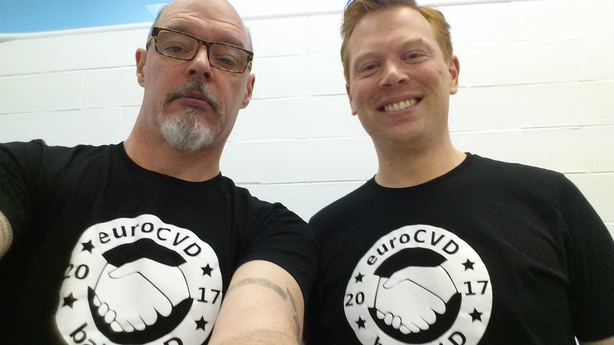
Here is a collection of ALD and CVD Fanatics sporting the 2017 Euro CVD / Baltic ALD official T-shirt.


Matt "the golden boy" has bought the @euroCVD #BalticALD T-shirt and is #ontheroadtolkpg #cvdald17.

Order your T-shirt here for only 18.99€


Sean and Henrik showing of their T-shirts 


Another bald guy with the t-shirt.

Prof. Dr. Seán Barry - Born to Finland, Born to ALD Gold

Here is a long audio interview and a partial transcript with the Canadian Prof. Seán Barry, the Department of Chemistry at Carleton University. Seán is known for many great things, one of them being ALD of Gold and another is his love for Finland and the wonderful Finns and Finnish culture.

"Dr. Seán Barry is a Professor in the Department of Chemistry at Carleton University. He received his B.Sc. in Chemistry from Queen’s University at Kingston and was awarded his PhD in Inorganic Chemistry from the University of Ottawa. Next, Seán conducted postdoctoral research at the University of Bourgogne in France, Cornell University, and Harvard University. Seán served as a Lecturer at the University of Ottawa and a Visiting Scholar at Harvard University before joining the faculty at Carleton University where he is today. Seán is here with us today to tell us all about his journey through life and science."
"One of Seán’s favorite travel destination is Helsinki. He has been there now many times, but the first time he went, Seán was completely blown away by the city’s beauty. Helsinki has great music, excellent food, and wonderful people. In particular, Seán remembers going to a restaurant called Garlic where everything on the menu contained garlic. While he wasn’t a fan of the garlic beer, the garlic ice cream was surprisingly delicious." [photo by Riikka Puurunen, Moscow]

 Finns and Canadians are the two nations most crazy about ice Hockey.
Later this year Prof. Barry will be heading to Sweden for a term as visiting Professor at Linköping University and co-organizing the 2017 EuroCVD - Baltic ALD Conference. and therefore he has recently been awarded a Vinnova VINNMER Mobility grant to group 13 nitrides in Sweden starting in July 2016. Prof. Henrik Pedersen, Linköping University, and Chair of the conference is right now visiting Barry Lab at Carleton and will be going back with Seán to Sweden.

Prof. Barry and Prof. Pedersen sporting the EuroCVD / Baltic ALD official T-shirts, order your own here.

2016 Growth Expected - Gas Landscape Shifting


 Buy Reports  | CMC Fabs   |  CMC Seminars  |  About US
2016 Growth Expected:
Gas Landscape Shifting
     The 2016 Gas Market is expected to total $3.9 billion, growing ~7% from 2015, as stated in the recently released Critical Materials Report on Electronic Gases by TECHCET. Changes in the market dictate shifts in supplier share, as highlighted in the report, along side supply & demand concerns relating to NF3, WF6, He, Ne, etc.

    Over the next five years, China is investing ~$100B, in attempts to develop a vertically integrated electronics industry.  The "end game" is to make China self-sufficient with regard to every portion of the electronics supply chain, including materials.  This is already having a significant impact on foreign companies trying to do business in China. Details on the China Materials Supply Chain and Competitive Issues can be found in TECHCET's 2016 Critical Materials Reports
     The N
eon Shortage is the hot topic of the year, with both supply and demand issues causing great concern. The shortage is forecasted to last the next 5-7 years, mostly due to the delay in implementing EUV lithography into commercialization. Details can be found in TECHCET's 2016 Neon Supply and Demand Report.
     The neon shortage has pushed DUV laser manufacturers, Cymer and Gigaphoton, to develop neon reduction strategies to help their customers. These will help, however, they will not be enough to curtail the upcoming shortage.         
 
For more information, please contact cmcinfo@techcet.com or call 1-480-382-8336
 
* Interested in learning more about China's supply chain? *
Don't miss out on October's CMC Seminar in China!

Saturday, June 11, 2016

Strem offer re-usable bubblers for use in ALD and CVD

As reported by Strem in Cambridge Network: Strem in Ireland and the UK continues not only to provide a wide variety of high purity precursors and several cylinder options, but also strives to build ongoing relationships with its customers by offering fast refilling and cleaning services


Researchers investigating chemical vapour deposition (CVD) would certainly call this field of study a mature research area. The field has grown significantly, with the addition of single atomic layer deposition ALD, from the early days of the mid to late 1980s where precursors had to be synthesized in-house to then decompose by gentle (more or less gentle) thermal treatment.

Rapid developments associated with CVD/ALD derived materials can surely be associated with the ever increasing number of volatile organometallic and inorganic – some may consider them as simple coordination complexes- that are commercially available.

Applications ranging from high dielectric oxides or transparent conductive films within electronics to protective coatings for clothing. The materials include high purity silicon-containing reagents to volatile rare-earth precursors.

Strem has been involved in this field for quite some time and an extensive list of compounds are available for use in CVD/ ALD related chemistry. Customers' containers or custom bubblers/cylinders are designed to be compatible with commercial equipment. These easily connected units made of stainless steel, come pre-charged with your favourite material and represent a plug-and-play approach to the once tedious synthetic task of actually making and handling such volatile and often harmful materials.

Many universities and companies find they are unable to refill their bubblers purchased, but this is a service Strem UK can offer.

How a Flat Panel Display Works - An inside look

Here is an excelletn visual description oon "How a Flat Panel Display Works" that can be very useful for all of you into ALD ultra barriers for display applications:


"Ever wonder how your flatscreen television works? Well now you can take an inside look into the inner works of a flatscreen display!... READ MORE.

RASIRC Study Finds 500 Fold Particle Reduction Using RASIRC RHS versus Flash Vaporizer

RASIRC Study Finds 500 Fold Particle Reduction Using RASIRC RHS versus Flash Vaporizer Low particle count pivotal to processing nanoscale features in new semiconductor devices.

San Diego, Calif – June 7, 2016 –RASIRC today announced that a new study shows that the RASIRC RainMaker® Humidification System (RHS) generates substantially lower particle count than flash vaporizers. The study compared particle generation in thermal and membrane evaporation systems using water. Particles are hazardous to microelectronics, causing defects and reduced electrical performance. Shrinking device sizes have made even the smallest particles and microdroplets into killer particles. The RASIRC RHS generates and delivers precise amounts of ultrapure water vapor for atomic layer deposition (ALD) and other semiconductor processes.
 Figure 1. Illustration of Membrane Technology Pervaporation process.

“Particle problems frequently arise when vaporizers are used to create gases from liquid sources,” said Jeff Spiegelman, RASIRC President and Founder. “Our pervaporization technology keeps liquid and gas separate by using a non-porous membrane. This technology demonstrates a particle-free vapor instead of a constant stream of particles that is generated with current vaporizer technology.” A principal drawing of the RHS device is shown in Figure 1 above. The study compared the relative particle/microdroplet generation of pervaporation versus flash vaporization in both continuous and intermittent flow conditions. A liquid evaporation vaporizer (LE), also known as a flash vaporizer, was compared to the RHS. Particles down to 10 nanometer size were measured by a condensation particle counter using water vapor as the condensation gas.

I asked Jeff Spiegelman about what motivated RASIRC to conduct this study and he responded “There has long been a debate on whether micro-droplets truly exist is a gas stream.  This study proves that they do exist and can be created or prevented through proper engineering.  Completely vaporizing a micro droplet in an ALD chamber is a thermodynamic challenge, by replacing flash vaporizers with membrane vaporizers this problem is prevented."  
Figure 2. Comparison of RHS and LE. LE internal temperature at 140°C. Overall, LE created 400 to 500 times more particles per minute.

Results (Figure 2) in continuous flow testing showed that the RHS was substantially more effective than the LE. The LE created 400-500 times more particles per minute than the RHS. In intermittent flow conditions, testing showed that the RHS was insensitive to flow interruptions while flash vaporizers created spikes of up to 5,000 on initiation of flow.

“Incomplete vaporization is the fundamental problem for flash vaporizers, causing spikes and a continuous stream of entrained microdroplets,” said Spiegelman. “The RHS operates at lower temperatures and adds water vapor directly to the carrier gas, reducing particle count reaching wafers and thereby improving film uniformity.”

Previous testing indicated that the RHS is feasible for ALD. In that testing, the RHS was able to achieve expected layer thickness and there were no obvious particle difference with a standard ozone plasma process.

Thursday, June 9, 2016

Check out this demo of the Lumineq TASEL made by ALD

At the end of 2012, Beneq acquired the Finnish-based electroluminescence business from US Planar Systems, Inc. The new display product brand is called Lumineq. Together with Beneq, Lumineq works closely on the industrial production and development of TASEL and TFEL technology and other atomic layer deposition (ALD) enabled products. The displays are ideal for high-end applications, where a subtle look and first-class viewing experience make the product stand out. 

Below is a new demo video of an Lumioneq TASEL display in action driving down a challenging road. It would be raelly cool if you could get one of those from Tom Tom or Garmin for any car.


ALD functionalization with ZnO generates CNTs that possess increased risk for human exposure

Here is a study on the risks of novel nano materials and in this parrticular case ZnO ALD coated multi walled carbon annotuber (MWCNTs). The study concludes that  "Pulmonary exposure to ZnO-coated MWCNTs produces a systemic acute phase response that involves the release of Zn+2, lung epithelial growth arrest, and increased IL-6. ALD functionalization with ZnO generates MWCNTs that possess increased risk for human exposure." So basically be very careful in the lab and use gloves, lab coat, safety glaces and and a mask when handling your new smart nano materials since there is no way you can tell if what you have synthesised is a potent risk for you and your surroundings. The study is OPEN ACCESS and free to download as below.

Atomic layer deposition coating of carbon nanotubes with zinc oxide causes acute phase immune responses in human monocytes in vitro and in mice after pulmonary exposure


Erinn C. Dandley, Alexia J. Taylor, Katherine S. Duke, Mark D. Ihrie, Kelly A. Shipkowski, Gregory N. Parsons and James C. Bonner
Particle and Fibre Toxicology 201613:29, DOI: 10.1186/s12989-016-0141-9 [OPEN ACCESS]

 
Background

Atomic layer deposition (ALD) is a method for applying conformal nanoscale coatings on three-dimensional structures. We hypothesized that surface functionalization of multi-walled carbon nanotubes (MWCNTs) with polycrystalline ZnO by ALD would alter pro-inflammatory cytokine expression by human monocytes in vitro and modulate the lung and systemic immune response following oropharyngeal aspiration in mice.
 
Methods

Pristine (U-MWCNTs) were coated with alternating doses of diethyl zinc and water over increasing ALD cycles (10 to 100 ALD cycles) to yield conformal ZnO-coated MWCNTs (Z-MWCNTs). Human THP-1 monocytic cells were exposed to U-MWCNTs or Z-MWCNTs in vitro and cytokine mRNAs measured by Taqman real-time RT-PCR. Male C57BL6 mice were exposed to U- or Z-MWCNTs by oropharyngeal aspiration (OPA) and lung inflammation evaluated at one day post-exposure by histopathology, cytokine expression and differential counting of cells in bronchoalveolar lavage fluid (BALF) cells. Lung fibrosis was evaluated at 28 days. Cytokine mRNAs (IL-6, IL-1β, CXCL10, TNF-α) in lung, heart, spleen, and liver were quantified at one and 28 days. DNA synthesis in lung tissue was measured by bromodeoxyuridine (BrdU) uptake.

Results

ALD resulted in a conformal coating of MWCNTs with ZnO that increased proportionally to the number of coating cycles. Z-MWCNTs released Zn+2 ions in media and increased IL-6, IL-1β, CXCL10, and TNF-α mRNAs in THP-1 cells in vitro. Mice exposed to Z-MWCNTs by OPA had exaggerated lung inflammation and a 3-fold increase in monocytes and neutrophils in BALF compared to U-MWCNTs. Z-MWCNTs, but not U-MWCNTs, induced IL-6 and CXCL10 mRNA and protein in the lungs of mice and increased IL-6 mRNA in heart and liver. U-MWCNTs but not Z-MWCNTs stimulated airway epithelial DNA synthesis in vivo. Lung fibrosis at 28 days was not significantly different between mice treated with U-MWCNT or Z-MWCNT.

Conclusions

Pulmonary exposure to ZnO-coated MWCNTs produces a systemic acute phase response that involves the release of Zn+2, lung epithelial growth arrest, and increased IL-6. ALD functionalization with ZnO generates MWCNTs that possess increased risk for human exposure.

Wednesday, June 8, 2016

Beneq see growth in ALD services and foundry ALD production

Beneq are reporting that a growing part of their business comes from services - that is ALD coating services. Beneq calls this Thin as a Service™ a complete thin film service solution that provides you with a quick and easy way to implement a new coating solution from the first samples to full-blown production

Beneq reports in their News Blog: A growing part of Beneq’s business comes from services. Our complete thin film service concept, Thin as a Service, which we launched last year, has been received well. The customers seem to appreciate the possibility to get a quick proof of concept of new ALD applications with ALD-123 as well as the shorter time to production enabled by our Coating Services.

There seems to be a new app in the process in our Services business unit every time you ask, and they are really interesting. To give you a better understanding about the fascinating variety of ALD applications, we have added new ALD customer cases on our Applications pages:

1) Moisture barriers for flexible and organic electronics is one of the hot topics in industrial ALD and OLED encapsulation is the hottest application.

2) Another moisture barrier application we have done several versions of is protection of scintillator plates. Scintillators are typically used in the panels of digital x-ray machines for capturing the image and they require humidity barriers, which are difficult to apply because the surface of the plates is so uneven.

3) Optical coatings is another growth area for industrial ALD. The applications in this area range from decorative coatings to demanding optical filters. A great example is NIR filters inside a tube, which are in practice impossible to create without ALD.

4) Most of the projects in Beneq Development Services are the starting point on a way towards a new industrial ALD application, but the projects can also be outsourced research projects. Sometimes we just perform ALD material research for our customers.

We will be sharing more customer project examples later. If you are interested in where atomic layer deposition can be used, remember to visit our Applications pages regularly or contact us to hear all about the latest apps. There are always new updates available at your ALD App Store.

CMC Meeting October – China Supply Chain

“CMC Meeting October – China Supply Chain”


 Interested in Participating?

I. October 2016, CMCFabs 1-Day Seminar in China- Focused on the China Supply Chain
II. May 2017: 2nd Annual Critical Materials Conference in Texas
or
III. Interested in the benefits of an Associate Membership? Please Contact us at cmcinfo@TECHCET.com 


 *PRESENTATIONS FROM CMC CONFERENCE AVAILABLE for ATTENDEES/REGISTRANTS*

For login information please contact cmcinfo@TECHCET.com

Novel energy inside a microcircuit chip: VTT developed an efficient nanomaterial-based integrated energy storage

Here is a cool energy storage device from VTT in Finland using Finnish ALD technology from Beneq - a Beneq TFS-500 reactor.
As published by VTT: VTT Technical Research Centre of Finland developed an extremely efficient small-size energy storage, a micro-supercapacitor, which can be integrated directly inside a silicon microcircuit chip. The high energy and power density of the miniaturized energy storage relies on the new hybrid nanomaterial developed recently at VTT. This technology opens new possibilities for integrated mobile devices and paves the way for zero-power autonomous devices required for the future Internet of Things (IoT).

Supercapacitors resemble electrochemical batteries. However, in contrast to for example mobile phone lithium ion batteries, which utilize chemical reactions to store energy, supercapacitors store mainly electrostatic energy that is bound at the interface between liquid and solid electrodes. Similarly to batteries supercapacitors are typically discrete devices with large variety of use cases from small electronic gadgets to the large energy storages of electrical vehicles.
The energy and power density of a supercapacitor depends on the surface area and conductivity of the solid electrodes. VTT's research group has developed a hybrid nanomaterial electrode, which consists of porous silicon coated with a few nanometre thick titanium nitride layer by atomic layer deposition (ALD). This approach leads to a record large conductive surface in a small volume. Inclusion of ionic liquid in a micro channel formed in between two hybrid electrodes results in extremely small and efficient energy storage.

The new supercapacitor has excellent performance. For the first time, silicon based micro-supercapacitor competes with the leading carbon and graphene based devices in power, energy and durability.


From Graphical abstract - Conformal titanium nitride in a porous silicon matrix: A nanomaterial for in-chip supercapacitors, Nano Energy26(2016)340–345, doi:10.1016/j.nanoen.2016.04.029
Micro-supercapacitors can be integrated directly with active microelectronic devices to store electrical energy generated by different thermal, light and vibration energy harvesters and to supply the electrical energy when needed. This is important for autonomous sensor networks, wearable electronics and mobile electronics of the IoT.

VTT's research group takes the integration to the extreme by integrating the new nanomaterial micro-supercapacitor energy storage directly inside a silicon chip. The demonstrated in-chip supercapacitor technology enables storing energy of as much as 0.2 joule and impressive power generation of 2 watts on a one square centimetre silicon chip. At the same time it leaves the surface of the chip available for active integrated microcircuits and sensors.

VTT is currently seeking a party interested in commercializing the technique.

VTT's article on integrated energy storage will be published in Nano Energy magazine (Volume 26, August 2016, pages 340-345). The article can be read online: http://dx.doi.org/10.1016/j.nanoen.2016.04.029

Ultratech Cambridge Nanotech Enter Into JDP With IMEC To Study Area-Selective Deposition Technology

SAN JOSE, Calif., June 8, 2016 /PRNewswire/ -- Ultratech, Inc. (Nasdaq: UTEK), a leading supplier of lithography, laser­ processing and inspection systems used to manufacture semiconductor devices and high-brightness LEDs (HB­ LEDs), as well as atomic layer deposition (ALD) systems, announced that its Cambridge Nanotech business unit Ultratech-CNT has entered into a Joint Development Program (JDP) with IMEC in the field of Area-Selective Deposition (ASD) technology. The ASD project will concentrate on the study and use of Self-Assembled Monolayers (SAMs) as a means of functionalizing surfaces to selectively inhibit ALD-grown films. Ultratech-CNT's Savannah S300 ALD system will be used for this project to explore the use of SAMs and ALD films on 300-mm wafers using a single platform. 


Laurent Lecordier, Ph.D., senior research scientist at Ultratech-CNT, has been active in research that combines SAMs and ALD. According to Lecordier, "The broader implications of this technology suggest that we will not only be able to address the field of ASD, but we will also be able to make positive contributions in industrially-relevant areas, such as low-k pore filling, work function modifications, and surface energy tuning. With the JDP in place, I am very much looking forward to participating in this work, which has garnered strong industrial and academic interest."


Given the large potential for producing disruptive applications using the combined SAMs and ALD system, (including ASD, low-k pore filling, work function modifications, surface energy tuning, and novel materials growth), Ultratech-CNT believes this collaborative program will yield high impact results.


Savannah S300 ALD System
The Savannah family of ALD systems (S100, S200, S300) has become the preferred system for university researchers worldwide engaged in ALD and looking for an affordable yet robust platform. With a wide array of process oriented options, such as low vapor pressure precursor delivery, and plasma, along with a range of real-time analytical options such as in-situ ellipsometry, in-situ quartz crystal microbalance, and mass spectrometry -- the Savannah enables the serious researcher to deposit and study a broad spectrum of single and multi-component ALD films and Self-assembled Monolayers. With over 1000 peer-reviewed journal publications referencing its ALD systems, Ultratech-CNT's ALD instruments maintain a leading position as the tools-of-choice among active researchers.

Saturday, June 4, 2016

2nd Generation Spatial ALD from SoLayTec

The article is both in Chinese and English
Last December SoLayTec celebrated its 5th anniversary, and in the meantime has installed about twenty items of ALD equipment in the PV industry. We are happy to be the leading ALD supplier in this market. Unfortunately, while we are not yet number one in the market for Al2O3 passivation, we do expect to win further market share with our 2nd generation ALD system. As we all know, a successful product is based not only on the right timing of the market introduction but also on its uniqueness and user-friendliness. After installing machines at various PV manufacturers, we started to learn about the pros and cons of our system. In this article I would like to explore both these topics and convince you to become one of our next ALD users.
"Published PES magazine edition PES Solar China issue 2016"
- See more at: http://www.solaytec.com/publications#sthash.ni8K3irp.dpuf
Here is an article in both in Chinese and English about recent progress by SoLayTec and the 2nd generation Spatial ALD technology they are bringing to the PV ALD Al2O3 backside passivation market.

Last December SoLayTec celebrated its 5th anniversary, and in the meantime has installed about twenty items of ALD equipment in the PV industry. We are happy to be the leading ALD supplier in this market. Unfortunately, while we are not yet number one in the market for Al2O3 passivation, we do expect to win further market share with our 2nd generation ALD system. As we all know, a successful product is based not only on the right timing of the market introduction but also on its uniqueness and user-friendliness. After installing machines at various PV manufacturers, we started to learn about the pros and cons of our system. In this article I would like to explore both these topics and convince you to become one of our next ALD users.


You may have noticed that it rains a lot across Europe this early summer. Here is a picture form the other day when I test the SoLayTec spatial ALD technology.


"Published PES magazine edition PES Solar China issue 2016"

- See more at: http://www.solaytec.com/publications#sthash.ni8K3irp.dpuf

The article is both in Chinese and English
Last December SoLayTec celebrated its 5th anniversary, and in the meantime has installed about twenty items of ALD equipment in the PV industry. We are happy to be the leading ALD supplier in this market. Unfortunately, while we are not yet number one in the market for Al2O3 passivation, we do expect to win further market share with our 2nd generation ALD system. As we all know, a successful product is based not only on the right timing of the market introduction but also on its uniqueness and user-friendliness. After installing machines at various PV manufacturers, we started to learn about the pros and cons of our system. In this article I would like to explore both these topics and convince you to become one of our next ALD users.
"Published PES magazine edition PES Solar China issue 2016"
- See more at: http://www.solaytec.com/publications#sthash.cRQOwaBN.dpuf