Thursday, March 10, 2016

ASM International recieves Intel´s preferred quality suplier award

ASM International has been recognized as one of 26 companies receiving Intel Corporation's Preferred Quality Supplier (PQS) award for their performance in 2015. ASM International has demonstrated industry-leading commitment across all critical focus areas on which they are measured: quality, availability, technology, customer service, labor and ethics systems and environmental sustainability. 


ASM International is recognized for their significant contributions providing Intel with front-end deposition equipment for ALD, PECVD and Diffusion, viewed as essential to Intel's success.
 

Atomic Layer Lithography turns ALD into an angstrom-resolution gap-forming method

Here is a really cool paper on Atomic Layer Lithography! The method is a combination of "atomic layer lithography, which turns atomic layer deposition (ALD) into an angstrom-resolution gap-forming method" The combination of these two powerful methods can create ultrasmall coaxial nanocavities at extreme densities over an entire wafer, opening up the door to devices with sub-10 nm gaps"

High-Throughput Fabrication of Resonant Metamaterials with Ultrasmall Coaxial Apertures via Atomic Layer Lithography


Daehan Yoo, Ngoc-Cuong Nguyen, Luis Martin-Moreno, Daniel A. Mohr, Sol Carretero-Palacios, Jonah Shaver, Jaime Peraire, Thomas W. Ebbesen, and Sang-Hyun Oh

Nano Lett., 2016, 16 (3), pp 2040–2046 DOI: 10.1021/acs.nanolett.6b00024

Figure from graphical abstract used with permission (Account #: 3000915597)
We combine atomic layer lithography and glancing-angle ion polishing to create wafer-scale metamaterials composed of dense arrays of ultrasmall coaxial nanocavities in gold films. This new fabrication scheme makes it possible to shrink the diameter and increase the packing density of 2 nm-gap coaxial resonators, an extreme subwavelength structure first manufactured via atomic layer lithography, both by a factor of 100 with respect to previous studies. We demonstrate that the nonpropagating zeroth-order Fabry-Pérot mode, which possesses slow light-like properties at the cutoff resonance, traps infrared light inside 2 nm gaps (gap volume ∼ λ3/106). Notably, the annular gaps cover only 3% or less of the metal surface, while open-area normalized transmission is as high as 1700% at the epsilon-near-zero (ENZ) condition. The resulting energy accumulation alongside extraordinary optical transmission can benefit applications in nonlinear optics, optical trapping, and surface-enhanced spectroscopies. Furthermore, because the resonance wavelength is independent of the cavity length and dramatically red shifts as the gap size is reduced, large-area arrays can be constructed with λresonance ≫ period, making this fabrication method ideal for manufacturing resonant metamaterials.

Wednesday, March 9, 2016

Finland’s first satellite is protected by Beneq ALD

Beneq reports that about entering space with their ALD technology. Aalto-1 is a student satellite project, created by an interdisciplinary co-operation network within Aalto University, with the satellite's payloads developed in Technical Research Centre of Finland VTT, Helsinki University, Turku University and Finnish Meteorological Institute FMI. The team has members from five different departments of Aalto University. Additionally, a consortium of Finnish universities and space industry has been formed to support the satellite project, and international relations with several foreign universities have been created.


The historic rocket launch by the company SpaceX will carry the satellite into space later in spring 2016. In addition to Aalto-1, the rocket will bring a record number of nanosatellites into orbit at 600km.(http://www.aalto.fi/en/current/news/2016-03-02/)

On the satellite, there are areas that are not covered by solar cells or any other equipment, which still need protection. The solution is a two-layer coating, where the aluminium surfaces have first been anodized and then coated in the Beneq factory with indium tin oxide (ITO).

CMC Conference 2 Weeks Left for Early Registration!

“Critical Materials for Device Driven Scaling”

The Critical Materials Conference is a 2 day event providing actionable information on materials and supply-chains for current and future semiconductor manufacturing. Business drives the world, but technology enables semiconductor business, so we must understand the dynamics of how materials and technologies enable the scaling of devices in IC fabs. 


Conference speakers will provide information on critical materials used in HVM fabs, while also looking at manufacturing integration issues associated with new materials needed for future devices. Notable speakers from leading semiconductor fabricators, and materials companies, and leading market research firms will provide insights on this ever changing area of semiconductor process materials and markets.


2 Weeks Left to Register - Early Bird $349!

"Critical Materials for Device Driven Scaling"


Keynote Speaker
Tim G. Hendry
VP Technology & Manufacturing Group
Director, Fab Materials
Intel Corporation


"Material Requirements for the Future of Semiconductor Devices"


The Critical Materials Conference provides a structured framework to catalyze the flow of actionable technical and supply chain information related to critical materials.  Themes of the conference are centered around the needs of the Critical Materials Council (CMC) and the global IC fabrication industry. While executive conferences typically focus on the "what" and "why" of materials technologies, this conference will discuss "how" new materials can be controllably, safely, and cost-effectively used in fabs. The CMC Conference will also include market data to validate "when" materials will be used. Attendees from fabs, OEMs, and materials suppliers will network with peers and gain insights into best-practices of the entire supply-chain.


3 Key Sessions Focused on Semiconductor Materials and Technology:
I.   Global Issues and the Supply Chain
II.  Immediate Challenges of Materials & Manufacturing
III. Emerging Materials Challenges
Featuring Speakers from Semiconductor Materials Supply Chain:IC Fab Technologists, Materials and Equipment Suppliers, Market Analysts


Techcet LLC, PO Box 3056, Rancho Santa Fe, CA 92067
Sent by info@cmcfabs.org in collaboration with
Constant Contact

Monday, March 7, 2016

Fraunhofer IVV develops ultra barrier films using atomic layer deposition

According to a press release March 07, 2016 : The Fraunhofer Institute for Process Engineering and Packaging IVV will present its latest work on the manufacture of ultra barrier films for the flexible encapsulation of Organic Electronics (OEs) at the international LOPEC fair in Munich on 6-7 April 2016 (Hall B0, Stand 100). A plant for coating films by atomic layer deposition is currently being constructed at the institute. This will allow the Fraunhofer IVV to further reduce the permeability of films and offer new film products to industry.


Minimizing the permeability to water vapor and oxygen is the key to further successful optimization of high barrier films. Atomic layer deposition (ALD) is paving the way for this. This technology is suitable for roll-to-roll processes, so allowing high production efficiency. Furthermore the processing speed is similar to that of the vacuum processes currently used to manufacture the highest barrier films.


This new technology at the Fraunhofer IVV will be used for publicly funded R&D projects aimed at providing industry with customized solutions and R&D services in the area of process and material development.

The new atomic layer deposition technology coupled with the existing expertise of the Fraunhofer IVV in the area of high barrier films means that there are very promising opportunities for significantly improving the barrier properties of films and in the medium term meeting the barrier requirements for OLED encapsulation.

Sunday, March 6, 2016

ASML and IMEC EUV Progress at SPIE Advanced Lithography Conference 2016

EUV is making progress and to several reports it may be ready for 7nm. Here you can find a report in SemiWiki by Scotten Jones on "ASML and IMEC EUV Progress" from the recent SPIE conference (21-25 February 2016, San Jose, USA). According to the report, ASML has made clear progress in throughput:
  • ASML has 8 NXE 3300 systems in the field running at ~55wph. 
  • ASML has shipped NXE3350B systems with ~125wph performance. 
  • The NXE3400B will ship this year and is expected to be the production workhorse running at ~145wph.

In another paper "Comparison of EUV and 193i based patterning for advanced node integration" Imec compared EUV to current ArFi or 193ilithography for three cases showing a cost comparasion resulting in a win for EUV : LE3 > SADP > EUV.

Abstract: "In this work we compare the pattering integrity results of product like structures using EUV- and 193i-Lithography. Traditional 193i based lithography requires multiple litho-etch (LE) or pitch doubling techniques to reach sub resolution pitch. These however add additional films and steps in the pattering process, and introduces CD and overly variability. EUV offers the possibility of single print for advanced nodes with a reduced process flow. However EUV introduces pattering selectivity and uniformity challenges. The process flows, complexity and pattering results will be presented for EUV single exposure, 193i multiple Litho Etch (LE3), and 193i Spacer Assisted Double Pattering (SADP+Keep)."

According to Scotten Jones the detailed comparison was for these 3 cases:
  1. The litho-etch-litho-etch-litho-etch (LE3) process prints 42nm lines with 144nm pitch and then shrinks them with a total of 27 steps. 
  2. The SADP process creates 48nm lines on a 96nm pitch and then shrinks them with a total of 18 steps. 
  3. EUV creates 24nm lines in an 8 step process. 
"In summary EUV had the best overall performance, SADP + block was second best and LE3 the worst. The biggest issue for EUV was LER and he thinks that can be improved." concluded Scotten Jones

Too read further about SPIE I asloo recommend this piece by Ed Korczynski at Solid State Technology looking at many additional papers presented at SPIE 2016:

http://semimd.com/blog/2016/03/03/many-mixes-to-match-litho-apps/

Photochemical atomic layer deposition and etching - Open Access Review

Here is a interesting review paper on photochemical activation of ALD and ALE processes by Prof. Paul Chalker from University of Liverpool [Thanks to Henrik Pedersen for this one]. The paper presents a review of the exploitation of light in ALD to stimulate photochemical processes. The use of light for area selective deposition for patterning methods is also reviewed and finally the potential for photo-etching in Atomic Layer Etching is assessed.


A range of radiation sources, which emit radiation at wavelengths below the visible (λ < 400nm) spectrum and into the UVA (315–400 nm, 3.10–3.94 eV), UVB (280–315 nm, 3.94–4.43 eV) and UVC (100–280 nm, 4.43–12.4 eV) ranges. [Surface & Coatings Technology 291 (2016) 258–263 Under a Creative Commons license]

ALE is the reverse process of ALD, i.e., the controlled layer-by-layer removal of material. Two examples are give of previous studies an photochemical ALE:
  • Photo-induced atomic layer etching of GaAs has been demonstrated using molecular chlorine (Cl2) coupled with KrF excimer laser irradiation (λ = 248 nm, 5 eV).
  • Etching of the reconstructed silicon, Si(111) 7 × 7 surface  using KrF excimer laser irradiation with Cl2 as the etchant.

Photochemical atomic layer deposition and etching

P.R. Chalker
Surface & Coatings Technology 291 (2016) 258–263
Under a Creative Commons license

Conventional atomic layer deposition (ALD) is a thermo-chemical process that is now used extensively in the manufacture of ultrathin films. In addition to substrate heating, various forms of other “assisted” ALD processes are actively being developed, where supplementary energy is supplied for example, from a plasma discharge or from light. This paper presents a critical review of the exploitation of light in ALD to stimulate photochemical processes. The range of light sources that are exploitable for photochemical ALD processes is considered and the chemical mechanisms that are stimulated in the ultraviolet spectrum are interpreted. The use of light as an excitation source lends itself to area selective deposition using lithographic methods or focused beams. The exploitation of photochemical processes for the deposition of patterned ALD films is reviewed in the context of the current alternatives. Finally, the potential for photo-etching is introduced. Atomic layer etching is a complimentary process to ALD and the application of photochemistry in layer-by-layer subtraction processes is considered.

Thursday, March 3, 2016

The Critical Materials Conference (CMC) announcement of speakers

The Critical Materials Conference is a 2 day event, May 5-6 in Hillsboro, OR, has now announced speakers!

Please check the Conference web for all information: http://cmcfabs.org/seminars/


May 4 (Wed, night)
5pm to 7pm, Evening Welcome Reception

May 5 (Thurs) - Day 1

Session I: Global Strategic Initiatives and the Supply Chain
Gus Richard -Northland Securities
Risto Puhakka – VLSI Research
Lita Shon-Roy – TECHCET
Keith Long - USGS
Open
Session II: Immediate Challenges of Materials & Manufacturing

Jim Feldhan - SEMICO
Bruce Adams - TECHCET
Bassam Elkhatib - Texas Instruments
Rob Nine - Pall Corp.
Jeff Hemphill - Intel

Unusual Round Table
Evening Reception: 5pm – 7pm

May 6 (Fri) - Day 2 (1/2 day)

Session II, continued, Immediate Challenges
Jean Marc Girard, Ph.D. - Air Liquide
S.I. Lee - Veeco

Session III: Emerging & Revolutionary Materials
Jan Vardaman – TechSearch International
Jonas Sundqvist, Ph.D. – TECHCET
John Smythe – Micron
David Thompson, Ph.D. - Applied Materials
Max Kelman, Ph.D. – Aixtron
Dave Roberts, Ph.D. – Nantero
Dan Alvarez, Ph.D. - Rasirc

Panel Discussion & Wrap-Up


Hosted by TECHCET

Wednesday, March 2, 2016

The first speakers for ALD 2016 in Dublin are announced!

Speakers and Conference Programme

Conference Speakers:

We are delighted to announce the first speakers for ALD 2016:
Please click on the bold speaker names to view their profile.


Speaker  Organisation  Presentation title
Raymond Adomaitis University of Maryland
Sumit Agarwal Colorado School of Mines, USA Plasma Physics and Diagnostics
Seán Barry Carleton University, Canada ALD Precursor Design & Synthesis
Robert Clark TEL America
Byung Joon Choi Seoul National University of Science and Technology Multi-layered selector and switch devices enabled by atomic layer deposition for crosspoint memory
Mike Cooke Oxford Instruments
Annelies Delabie IMEC Atomic layer processing of 2D materials for beyond CMOS applications
Jolien Dendooven University of Ghent Synchrotron-based characterization of Pt ALD
Mickael Gross-Jean ST Microelectronics
Joseph Hupp Northwestern University
Ying-Bing, Jiang University of New Mexico
Keren Kanarik Lam Research, USA Overview of Atomic Layer Etching
John Langan Air Products
Anatollii Malygin St Petersburg State Technological Institute
Yongfeng Mei Fudan University
Fred Roozeboom TU Eindhoven, The Netherlands Processing for 3D-IC Technologies
Lars Samuelson Lund University Nanowire-based Technologies for Electronics, LEDs and Solar-cells
Massimo Tallarida ALBA Synchrotron, Spain Characterization of ALD processes and Materials using Synchrotron Light
Stephan Wege Plasway GmbH, Germany Plasma Processing Reactor Design
Further speakers, profiles and the conference programme will be published soon.  Please check back for information.

March! 1 month left to avail of EARLY BIRD offer for ALD2016 in Dublin.

March! 1 month left to avail of EARLY BIRD offer for #ALD2016 in #Dublin.  View speaker line up & book places here - http://ald2016.com/


Welcome to the 16th Atomic Layer Deposition Conference


The 16th International Conference on Atomic Layer Deposition (ALD 2016) will be a three-day meeting dedicated to the science and technology of atomic layer controlled deposition of thin films. In every year since 2001, the conference has been held alternately in United States, Europe and Asia, allowing fruitful exchange of ideas, know-how and practices between scientists. This year, the ALD conference will incorporate the Atomic Layer Etching 2016 Workshop, so that delegates at the two events can interact freely. The conference will take place on 24-27 July 2016 at the Convention Centre Dublin, Ireland.

Tuesday, March 1, 2016

Lam Research gets into the booming ALD business and doubles their install base

 Yesterday Lam Research was covered in an in a Morgan Stanley Technology Conference. Here is a full playback as a webcast for those interested. For all you ALD guys the interesting stuff come in the last minute. Lam Research usually not talk a lot about ALD but here they came with an interesting statement.

Joe Moore from Morgan Stanley, semiconductor group asked Douglas R. Bettinger, chief financial officer of Lam Research about their ALD progress. "... we are very pleased with the progress we are making in atomic level deposition as well as the atomic level etch, which was the topic of Rick Gottscho, our head of global products talk at SPIE last week. I think we described exactly a doubling of the installed base last year in ALD; multiple customers. It's an ALD Oxide tool. Very pleased with our performance here. Three years ago, we didn't have any business in ALD and now we've got a meaningful amount of revenue coming from it."
Doug Bettinger is chief financial officer of Lam Research.(Lamresearch.com)
The ALD oxide tool is most probably the Vector - a multi-chamber or rather a multi-station tool within a single vacuum chamber. So it is not Spatial like Tuomo Suntolas first one, the new Applied Materials Olympia or the Jusung Engineering tools it is normal temporal ALD.

Monday, February 29, 2016

The BALD Engineering blog is growing in Asia

ALD is booming despite a flat year for semiconductor equipment spending because of investments for 10 nm that mean additional layers of ALD space defined multiple patterning compared to 14 nm. The BALD Engineering blog is growing in Asia recently - makes sense that´s where those ALD Fabs are located! Still though the top three is USA, France and Germany.


Also very existing -  I am very proud to welcome NCD an ALD Equipment Manufacturer from South Korea - the first blog sponsor from Asia. More to come on NCD in the next days!


Sunday, February 28, 2016

WoDIM 2016 Abstract Submission, Catania, Italy 27-30 June 2016

WODIM 2016, the 19th Workshop on Dielectrics in Microelectronics, which takes place from 27-30 June 2016 at the Hotel Baia Verde, Aci Castello (Catania), Italy. This event is hosted by the Italian National Research Council (CNR) - Institute for Microelectronics and Microsystems (IMM), and celebrates the 10th anniversary of the last time the workshop was held in Italy. 

Abstract Submission

Please send your 2 page abstract (including figures) preferably by e-mail (MS Word or pdf file) to wodim2016@imm.cnr.it, or e-mail to the Chair.

During submission include with the abstract the author information form.

Please state your preference for oral or poster presentation, as indicated in the author information form.

Submissions will be acknowledged and final notification will be sent in mid April 2016.


Veeco brings low temperature nitride Spatial FAST ALD to semiconductor manufacturing

Some years ago Veeco acquired a company founded by SI Lee, Synos Technology, who shipped a first Prototype System for FAST-ALD™ for OLED encapsulation to Samsung in 2013 (here). Since then Veeco has moved on from OLED taking this technology to the semiconductor wafer based manufacturing. Now Veeco report that they have demonstrated high-quality silicon nitride films at temperatures below 250 degrees using their FAST-ALD technology on customer wafers. They have garnered interest from multiple memory manufacturers and have started expanding their customer engagements for FAST-ALD technology.


“First of all, strong customer pull because they had an unmet need to put down silicon nitride at very low temperatures. And so we've seen strong customer pull from the customers and we've developed the deposition tools for that market and are generating very good film quality, so the things that our customers have told us they can't get with other approaches.” said John Peeler Veeco CEO in a recent Q4 2015 Results - Earnings Call (transcript by Seeking Alpha, see below).
Low temperature silicon nitride ALD is one of the fastest growing layer applications scaling down node by node for both Logic and Memory devices. Low temperature nitride can be employed for multi patterning techniques and growth is due to take over from LPCVD and PECVD as well as for new layer applications. According to John Peeler Veeco is also exploring partnerships with existing front-end semi equipment providers to commercialize this technology.

“We are looking to do it with a partner who is already established in that market. But that's what's caused us to keep investing, and I think you are right, ultimately it is a win-win, because we are either going to drive revenue and profit from a whole new application which I think will be a big benefit to us, or we'll say, we're going to get out of this because we can't make it successful.” Said John Peeler.

“In terms of how our R&D investments are distributed across various product lines, we generally do not provide a granular view on that. However, we are investing in ALD as John talked about and we are quite optimistic about that.” Said Shubham Maheshwari, CFO Veeco.


Brooks Automation CEO Stephen Schwartz see ALD growth for 10 nm

According to a recent Earnings call with Brooks Automation CEO Stephen Schwartz they see growth for 10 nm and ALD. Many ALD OMEs uses Brooks vacuum robotics to cluster their wafer based ALD process chambers, Two such examples are Jusung Engineering and Picosun.

It is also interesting and for sure also fantastic to see how ALD is often reported as its own business segment these days. Here is a good example on how Brooks Automation segments the market to Deposition, Etch and ALD. PVD and CVD is just bunched together into deposition with sol-gel and other - those guys are just not cutting edge anymore.


Brooks Automation, Inc.'s (BRKS) CEO Stephen Schwartz on Q1 2016 Results - Earnings Call Transcript (Seeking Alpha, available here) :

“We forecast growth in March driven by the same products and design wins that propelled us in 2015. Processes like Deposition, Etch and ALD which utilize our vacuum automation technology have exploded due to the numerous three dimensional device structures that have taken over leading-edge memory and logic designs and we are in the center of this space.”

ASM International's CEO Chuck Del Prado on 2015 ALD results

ASM International is the leading OEM for ALD and therefore interesting to follow in more detail. As announced here before on the ALD news blog, ASM International held an Q4/2015 earnings call on Wednesday 24 February. Here are some of the highlights with respect to ALD from that call. The full transcript of the call is available through Seeking Alpha (here). The webcast play back is also available at ASM´s web (here).

ASM International's (ASMI) CEO Chuck Del Prado on Q4 2015 Results:

“2015 was another year of success for our ALD business. Despite moderating conditions in the broader market during the year, momentum in the ALD market was again solid. On the back of a continued strong and leading position, we were able to take advantage of the growth in ALD demand, as evidenced by the double-digit growth in our net sales in 2015.“
  • ALD was again the key driver behind the growth in revenue in 2015 and accounted for clearly more than half of our total equipment revenue.
  • ASM has broadened their customer base beyond the traditional top three and had a growing contribution from the top 4 to top 10 customers.
  • The share of ALD of the total deposition equipment market will further increase.
  • More of the critical patterning steps at 10-nanometer will require spacer-defined double patterning based on single-wafer/mini-batch ALD.

Saturday, February 27, 2016

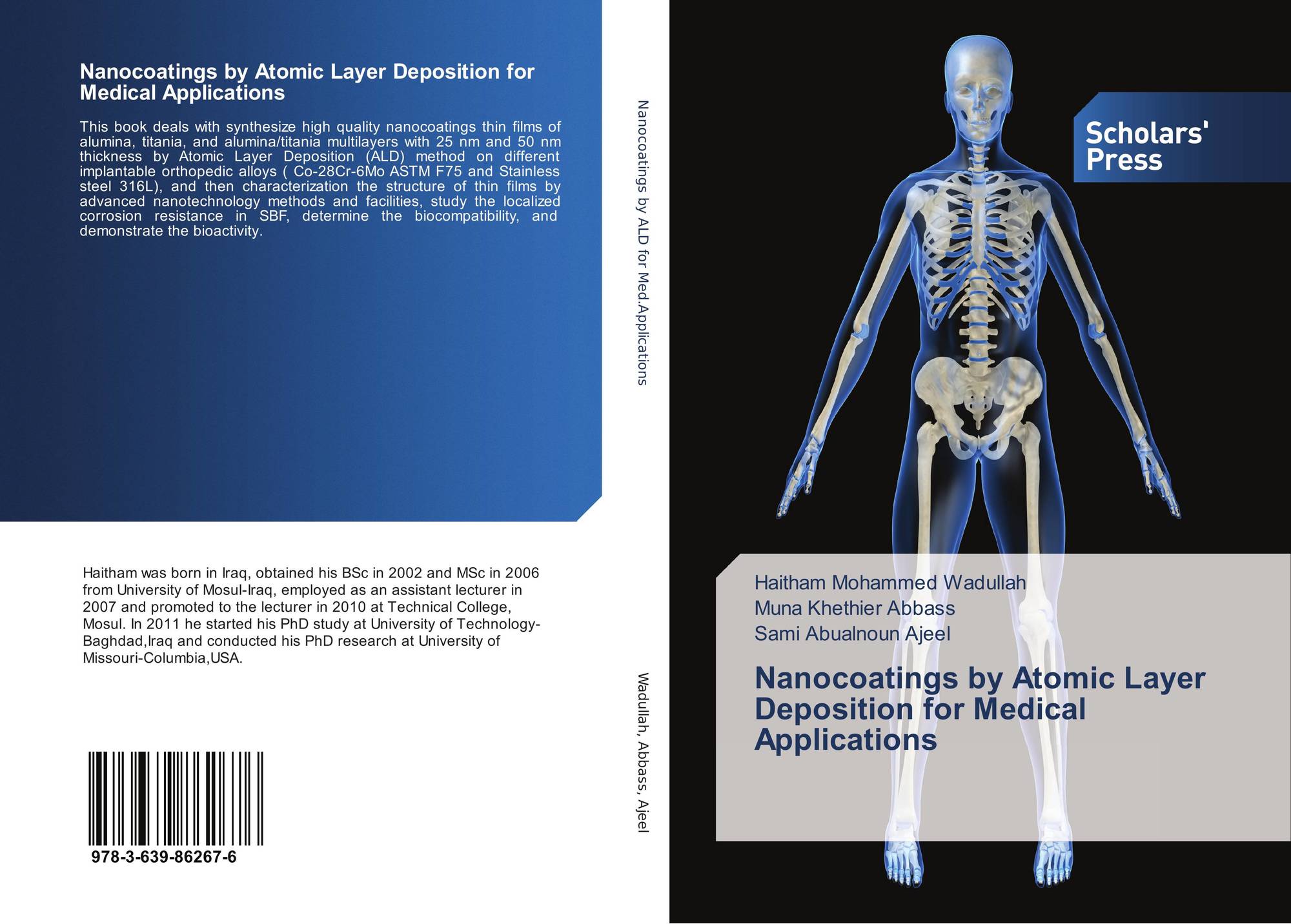
New Book - Nanocoatings by Atomic Layer Deposition for Medical Applications

Here is a new ALD book on ALD for medical applications as coatings for on different implantable orthopedic alloys:


This book deals with synthesize high quality nanocoatings thin films of alumina, titania, and alumina/titania multilayers with 25 nm and 50 nm thickness by Atomic Layer Deposition (ALD) method on different implantable orthopedic alloys ( Co-28Cr-6Mo ASTM F75 and Stainless steel 316L), and then characterization the structure of thin films by advanced nanotechnology methods and facilities, study the localized corrosion resistance in SBF, determine the biocompatibility, and demonstrate the bioactivity.

Book Details:

ISBN-13: 978-3-639-86267-6
ISBN-10:
3639862678
EAN: 9783639862676
Book language:
English
By (author) :
Haitham Mohammed Wadullah
Muna Khethier Abbass
Sami Abualnoun Ajeel

Number of pages:
192
Published on:
2016-01-15
Category:
Technology

Picosun 2016 ALD Product Brochures

Picosun has updated with 2016 version of their ALD Product line. Please find them all accessible below as pdf documents.

Picosun 2016 ALD Product Brochures

Picosun_brochure_2016_300mm_online
Picosun Brochure 300 mm Product Line

(pdf, 837 KB)
Picosun_brochure_2016_200mm_online
Picosun Brochure 200 mm Product Line

(pdf, 794 KB)

Thursday, February 25, 2016

Picosun continues strong growth and expands facilities

For those of you following this blog you know hat ALD is in a continous boom since some time. Picosun Oy, today announce thet they see a  strong growth and rapid expansion in the global industrial markets (Press release). Today Picosun has more than 50 emloyees and are growing. The company is actually twice the size of ASM Microchemistry today that was fully aquired by ASM International in 1999 (link).

The total value of the company’s new tool orders increased 41 % in the calendar year 2015. Picosun has been growing at a double-digit rate for several consecutive years. 
Team Picosun, today counting > 50 employees.

“We are happy that we got so many interesting new customers, but even happier we are with the growth of our repeat sales. It tells us that we have done lots of things right,” states Mr. Kustaa Poutiainen, Chairman of the Board and Chief Executive Officer of Picosun.

A significant part of the growth consisted of the deliveries of PICOPLATFORM™ vacuum cluster systems and automated PICOSUN™ P-series cassette loading batch tools to leading semiconductor industry customers in Asia and USA.

“Our aim is to produce ALD tools of the highest quality. They have been well received in industrial markets,” Mr. Poutiainen continues.

Picosun is also expanding its production capacity and personnel amount. In key role are especially the new subsidiaries in the central market areas such as Asia. The latest addition is the Japan unit starting in Q2/2016.

“Hiring new professionals, not only here in Finland but all over our worldwide subsidiary network, and extending our production facilities is crucial to enable even bigger success for our brand. The future looks bright for Picosun,” states Mr. Poutiainen.

Sunday, February 21, 2016

AVS Journal of Vacuum Science and Technology Recognizes Dr. Kaupo Kukli as One of its Most Valuable Reviewers (MVR)

AVS  Journal of Vacuum Science and Technology Recognizes  Dr. Kaupo Kukli 
as One of its Most Valuable Reviewers (MVR)
 
Here are recent JVST articles coauthored by Dr. Kaupo Kukli, University of Helsinki, available free for download during the next 30 days:
Dysprosium oxide and dysprosium-oxide-doped titanium oxide thin films grown by atomic layer depositionAile Tamm, Jekaterina Kozlova, Lauri Aarik, Jaan Aarik, Kaupo Kukli, Joosep Link and Raivo Stern
J. Vac. Sci. Technol. A 33, 01A127 (2015) |  Read More

Influence of precursor chemistry and growth temperature on the electrical properties of SrTiO3-based metal-insulator-metal capacitors grown by atomic layer depositionH. García, H. Castán, A. Gómez, S. Dueñas, L. Bailón, K. Kukli, M. Kariniemi, M. Kemell, J. Niinistö, M. Ritala and M. Leskelä
J. Vac. Sci. Technol. B 29, 01AC04 (2011) |  Read More
Behavior of zirconium oxide films processed from novel monocyclopentadienyl precursors by atomic layer depositionKaupo Kukli, Jaakko Niinistö, Aile Tamm, Mikko Ritala and Markku Leskelä
J. Vac. Sci. Technol. B 27, 226 (2009) | Read More 

Irradiation effect on dielectric properties of hafnium and gadolinium oxide gate dielectricsH. García, S. Dueñas, H. Castán, A. Gómez, L. Bailón, R. Barquero, K. Kukli, M. Ritala and M. Leskelä
J. Vac. Sci. Technol. B 27, 416 (2009) |  Read More
Electrical properties of thin zirconium and hafnium oxide high-k gate dielectrics grown by atomic layer deposition from cyclopentadienyl and ozone precursors
S. Dueñas, H. Castán, H. Garcia, A. Gómez, L. Bailón, K. Kukli, J. Niinistö, M. Ritala and M. LeskeläJ. Vac. Sci. Technol. B 27, 389 (2009) | Read More

Atomic layer epitaxy growth of aluminum oxide thin films from a novel Al(CH3)2Cl precursor and H2OKaupo Kukli, Mikko Ritala, Markku Leskelä and Janne Jokinen
J. Vac. Sci. Technol. A 15, 2214 (1997) | Read More

Saturday, February 20, 2016

New method using ALD enables storage and controlled release of pharmaceutical substances in the body

Maria Asplund from Sweden, since April 2013 appointed a Junior Group Leader for the Cluster of Excellence BrainLinks-BrainTools at the University of Freiburg and her doctoral candidate Christian Böhler has provided the foundations for a new molecular storage method using ALD. The method could find its way into clinical practice in the foreseeable future. 


The team have succeeded in creating a compound of organic and inorganic materials that is particularly well suited for the compact storage of pharmacologically active substances. The method involves an ALD ZnO layer that was deposited in a hot wall reactor OpAL - manufactured by Oxford Instruments. 

The full story is available here in PhysOrg and in the open access publication below. 

Please also check out earlier stories here on the ALD Blog on using ALD for controlled drug delivery from Nanexa of Sweden:

A Simple Approach for Molecular Controlled Release based on Atomic Layer Deposition Hybridized Organic-Inorganic Layers

Christian Boehler, Firat Güder, Umut M. Kücükbayrak, Margit Zacharias & Maria Asplund
Scientific Reports 6, Article number: 19574 (2016), doi:10.1038/srep19574 


The storage layer (marked green) can be used to store drugs; the surface layer (marked blue) enables their release in controlled dosages. Credit: Christian Böhler/University of Freiburg (Picture from PhysOrg: http://phys.org/news/2016-02-method-enables-storage-pharmaceutical-substances.html#jCp)

On-demand release of bioactive substances with high spatial and temporal control offers ground-breaking possibilities in the field of life sciences. However, available strategies for developing such release systems lack the possibility of combining efficient control over release with adequate storage capability in a reasonably compact system. In this study we present a new approach to target this deficiency by the introduction of a hybrid material. This organic-inorganic material was fabricated by atomic layer deposition of ZnO into thin films of polyethylene glycol, forming the carrier matrix for the substance to be released. Sub-surface growth mechanisms during this process converted the liquid polymer into a solid, yet water-soluble, phase. This layer permits extended storage for various substances within a single film of only a few micrometers in thickness, and hence demands minimal space and complexity. Improved control over release of the model substance Fluorescein was achieved by coating the hybrid material with a conducting polymer film. Single dosage and repetitive dispensing from this system was demonstrated. Release was controlled by applying a bias potential of ±0.5 V to the polymer film enabling or respectively suppressing the expulsion of the model drug. In vitro tests showed excellent biocompatibility of the presented system.

Thursday, February 18, 2016

RASIRC's water-free anhydrous hydrogen peroxide technology for ALD

Next week we at ALD Lab Dresden will meet up with Jeff Spiegelman, Founder and President of RASIRC to discuss some new technologies for delivery of difficult to deliver ALD co reactants. I am now happy to see the product release of the Brute Peroxide H2O2 (see press release below) is here. We had an early version of this on an ASM Pulsar 3000 some time ago here in Dresden. As you can see in the picture below the design you can fit this unit into basically any ALD gas box on the market  and just like that you have access to highly concentrated H2O2 - clever design indeed!


RASIRC released research results showing that anhydrous hydrogen peroxide gas enables a five-fold increase in surface hydroxyl density when compared to water in studies involving ALD nucleation on SiGe substrates. Hydroxyl density is an important factor in minimizing interfacial defects, increasing uniformity and improving next generation semiconductor device performance. BRUTE Peroxide provides a stable, reliable flow of anhydrous hydrogen peroxide for atomic layer deposition (ALD) and atomic layer etch (ALE). RASIRC products generate specialty gases from liquid sources to meet the demands of next generation semiconductor manufacturing.


BRUTE Peroxide generates water-free hydrogen peroxide gas and can be used with or without a carrier gas. Precursors that previously needed high temperatures or failed to grow uniform films with ozone, plasma, or water now have a new partner molecule for oxide film growth. BRUTE Peroxide is the only commercially available technology that can deliver up to 99.9% H2O2 gas by volume. Traditional H2O2 vaporizers, on the other hand, deliver less than 1% H2O2 gas by volume from standard H2O2 liquid source. (www.rasirc.com)


Next-generation devices are moving from Silicon to Silicon-Germanium Channels. It is critical to form a stable uniform oxides without Si or Ge dangling bonds on the interface grown by ALD at low temperatures. “Research proves conclusively that the presence of water in some ALD and ALE processes negatively affects interfacial layer uniformity, leading to higher defect density, slower initiation, and degraded performance,” said Jeffrey Spiegelman, RASIRC President and Founder. “Tests of BRUTE hydrogen peroxide confirm that removing the water during processing with dry H2O2 enabled a three-fold improvement in hydroxyl density compared to 30 percent H2O2 and water source.”

Full report: http://www.rasirc.com/news/releases/160216-RASIRC-Anhydrous-Hydrogen-Peroxide.htm

Veeco Instruments, imec Enter Development Deal for Gallium Nitride Epi Wafers

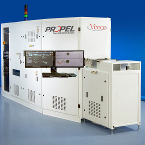
Veeco Instruments reported that it has signed a joint development project (JDP) agreement with imec, a Belgium-based nano-electronics research center, to accelerate the development of Gallium Nitride (GaN) based, power electronic devices using GaN Epi wafers. Under the development project, the GaN Epi wafers will be created using Veeco’s Propel Power GaN metal organic chemical vapor deposition (MOCVD) system. Veeco’s Propel® Power GaN MOCVD system.


Veeco’s Propel™ Power GaN MOCVD system is designed specifically for the power electronics industry. Featuring a single-wafer reactor platform, capable of processing six- and eight-inch wafers, the system deposits high-quality GaN films for the production of highly efficient power electronic devices. The single-wafer reactor is based on Veeco’s leading TurboDisc® design with breakthrough technology, including the new IsoFlange™ and SymmHeat™ technologies that provide homogeneous laminar flow and uniform temperature profile across the entire wafer. Customers can easily transfer processes from Veeco K465i™ and MaxBright™ systems to the Propel Power GaN MOCVD platform. (www.veeco.com)

Imec has already demonstrated significant gains in GaN layer uniformity and run-to-run repeatability with Veeco’s Propel system, resulting in significantly improved power device yields. The single wafer reactor incorporates Veeco’s proprietary TurboDisc® technology that delivers superior film uniformity, run-to-run control and defect levels compared to batch reactors.

Tuesday, February 16, 2016

VPHA ALD thesis list under construction

In the Virtual Project on the History of ALD (VPHA, http://vph-ald.com), we are collecting together a list of doctoral theses (PhD-equivalent) made on ALD worldwide. The list is planned to be published in the VPHA ALD History Review, Item #10 in the VPHA Publication Plan. Participation in VPHA is volunteer-based and open for everyone. 

More information: https://www.european-ald.net/news/ald-thesis-list-under-construction 

A nanolaser for fast and efficient data processing with light from TU München

As reported by TU Munich in EurekAlert!: Physicists at the Technical University of Munich (TUM) have developed a nanolaser, a thousand times thinner than a human hair. Thanks to an ingenious process, the nanowire lasers grow right on a silicon chip, making it possible to produce high-performance photonic components cost-effectively. This will pave the way for fast and efficient data processing with light in the future.
 

"Today already, transistors are merely a few nanometers in size. Further reductions are horrendously expensive," says Professor Jonathan Finley, Director of the Walter Schottky Institute at TUM. "Improving performance is achievable only by replacing electrons with photons, i.e. particles of light."

This news release is available in German.


Publications:

Monolithically Integrated High-beta Nanowire Lasers on Silicon
B. Mayer, L. Janker, B. Loitsch, J. Treu, T. Kostenbader, S. Lichtmannecker, T. Reichert, S. Morkötter, M. Kaniber, G. Abstreiter, C. Gies, G. Koblmüller, and J. J. Finley;
Nano Letters, 2016, 16 (1), pp 152-156 - DOI: 10.1021/acs.nanolett.5b03404

Coaxial GaAs-AlGaAs core-multishell nanowire lasers with epitaxial Gain control
T. Stettner, P. Zimmermann, B. Loitsch, M. Döblinger, A. Regler, B. Mayer, J. Winnerl, S. Matich, H. Riedl, M. Kaniber, G. Abstreiter, G. Koblmüller, and J. J. Finley;
Applied Physics Letters, 108, 011108 (2016) - DOI: 10.1063/1.4939549

Continuous wave lasing from individual GaAs-AlGaAs core-shell nanowires
B. Mayer, L. Janker, D. Rudolph, B. Loitsch, T. Kostenbader, Abstreiter, G. Koblmüller, and J. J. Finley; Applied Physics Letters 108, Vol. 8, to appear on Feb. 22nd (2016)