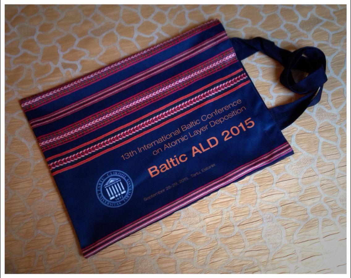
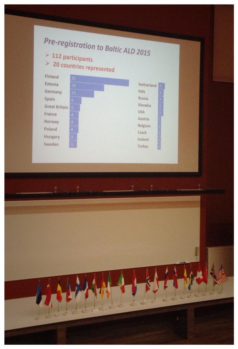
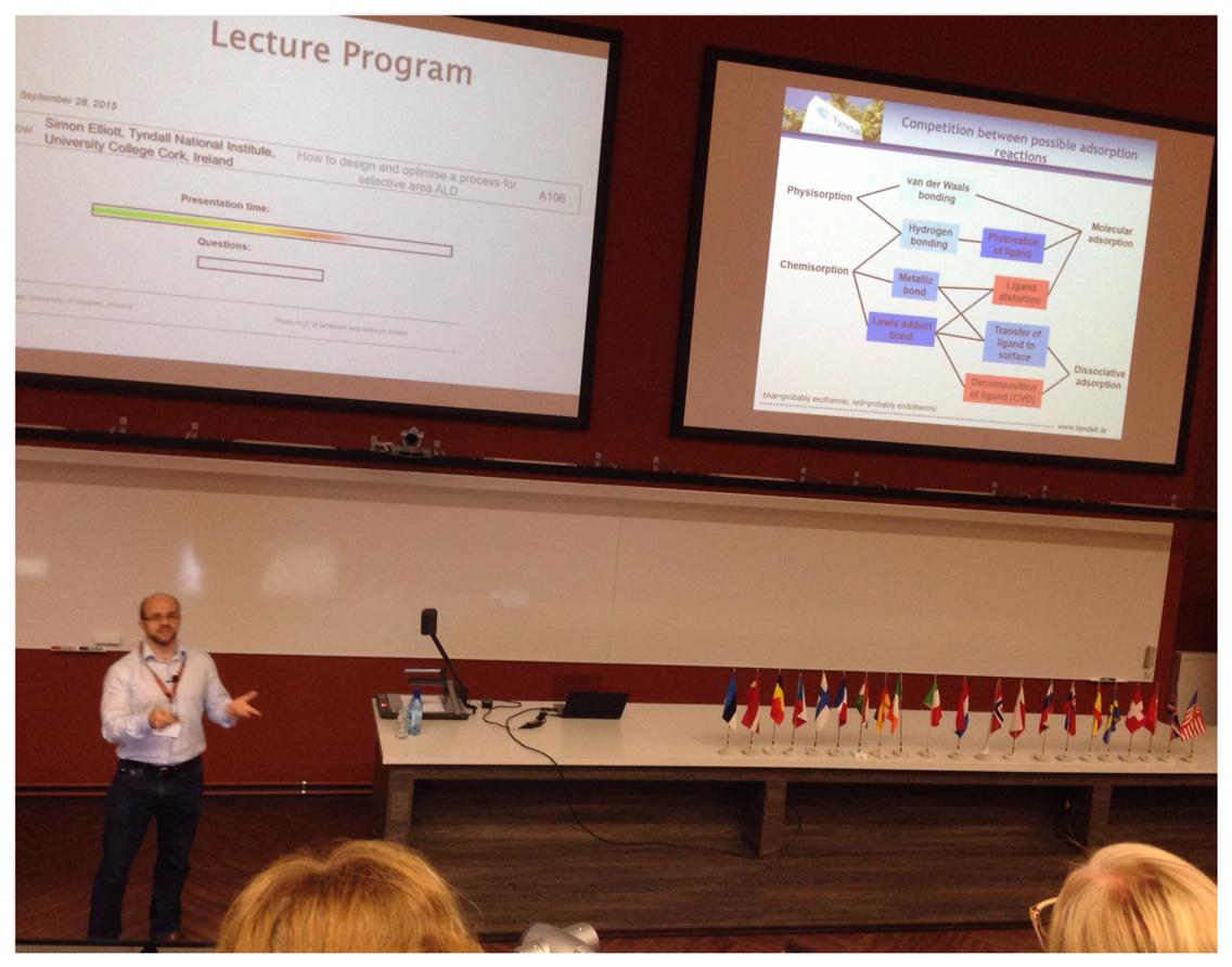
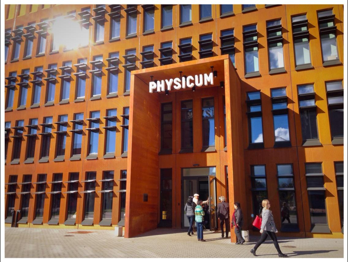
The Atomic Layer Deposition Russia 2015 (“ALD Russia”, in short) workshop was organized by Moscow Institute of Physics and Technology (MIPT), in Dolgoprudny, Moscow region, on September 21-23, 2015. The chairman of the workshop was Anatoly Malygin from St. Petersburg Technological Institute; Dr. Andrey Zenkevich and Dr. Andrey Markeev from MIPT were in charge of the local organizing committee. The workshop was opened by the rector of MIPT, corresponding member of RAS, professor Nikolay Kudryavtsev. According to the organizers, 67 people were registered to attend the workshop.
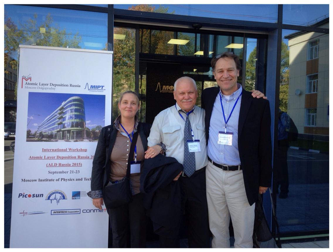
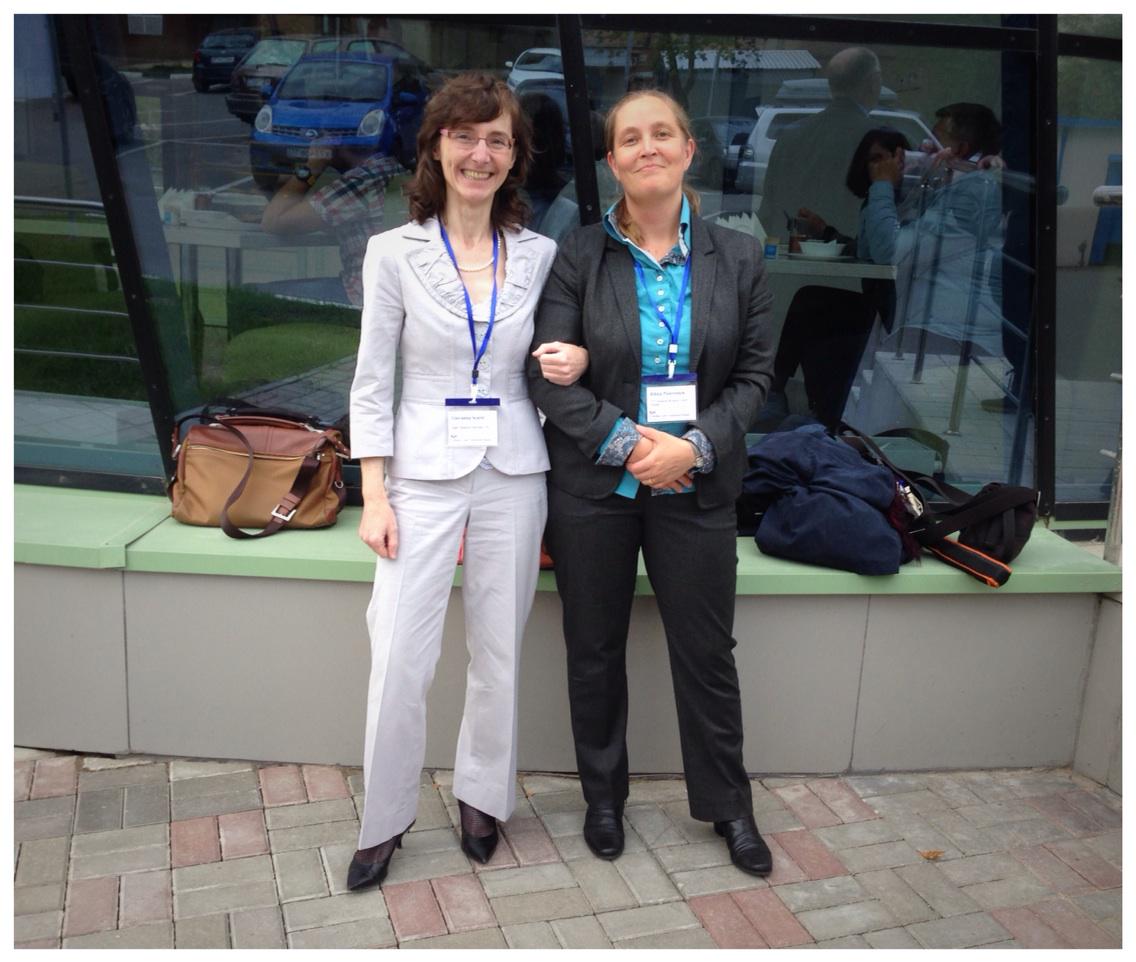
From left: Puurunen, Malygin, Parsons. Photographer: Abdulagatov (Riikka Puurunen, Twitter)
Invited speakers at the workshop were: Anatoly Malygin (St. Petersburg Technological University, Russia), Steven M. George (University of Colorado at Boulder, USA), Gregory N. Parsons (Carolina State University, USA), Riikka Puurunen (VTT Technical Research Centre of Finland), Annelies Delabie (IMEC, Belgium), Hyungjun Kim (Yonsei University, Korea), Cheol Seong Hwang (Seoul National University, Korea), Robert M. Wallace (University of Texas at Dallas, USA), Andrey Markeev (Moscow Institute of Physics and Technology, Russia), Sabina Spiga (Laboratorio MDM, IMM-CNR, Italy), Andrey Zenkevich/Yury Matveev (Moscow Institute of Physics and Technology, Russia), Vladimir Gritsenko (A. V. Rzhanov Institute of Semiconductor Physics of SB RAS, Russia), Ingo Dirnstorfer (NaMLab, Germany), Vladislav Vasilyev (Novosibirsk State Technical University and SibIS LCC, Russia), Giovanna Scarel (James Madison University, USA), Erwin Kessels (Eindhoven University of Technology, The Netherlands), Sean Barry (Carleton University, Canada), Svetlana Dorovskikh (A. V. Nikolaev Institute of Inorganic Chemistry SB RAS), and Evgeny Gornev (Mikron, Russia).
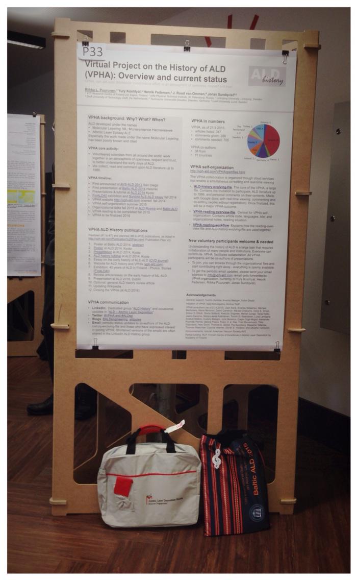
The scientific programme of the workshop was a balanced mixture of various subject areas, for example, ALD/PEALD precursor and process development, atomic layer etching, 2D materials, semiconductor applications, and thin film conformality analysis. Some truly futuristic talks were included in the programme, e.g. related to neural networks with ALD-grown memristors. There were also two talks that looked backwards in time: one on the historical developments of ALD under the name Molecular Layering in USSR/Russia; and one describing the organization of the on-going Virtual Project on the History of ALD (VPHA), a volunteer-based project where new participants are welcome and needed.
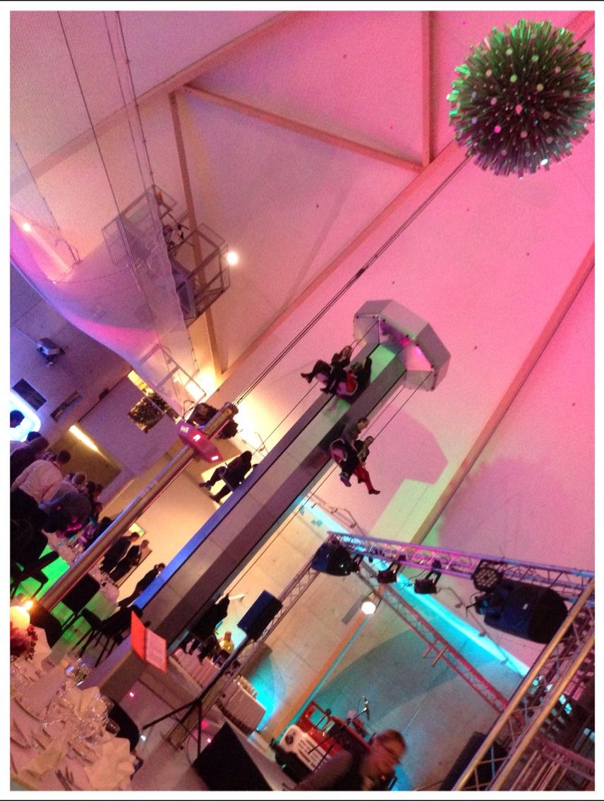
The non-scientific programme at the workshop consisted of a Moscow river cruise on Tuesday evening. The participants were transported with a bus from Dolgoprudny (through the well-known traffic jam of Moscow) to the centre of the city. With the private boat accompanied with a guide, the participants travelled along the Moskva river for about five hours, passing places such as Tretjagovskii Gallery, Kreml and the Red Square, and seeing also the statue of Peter the Great. At the boat, food was excellent and plenty. Many discussions were carried out in a forward-looking, pleasant sphere, and new connections made.
At the end of the workshop, the participants had a chance to visit the laboratories at MIPT.
As specified at the website
http://ald-conf.ru/, the goal of the workshop was to “consolidate the rapidly growing Russian ALD community, and to bring Russian researchers closer to leading international experts in the field.” In my view, this target was met: many leading scientists from Russia, several European countries, USA, Canada and Korea got together at the workshop, interacted during presentations, and enjoyed each other’s company at the social event.
With this travel report, I want to thank the organizers at MIPT for creating this unique event. I also express my thanks to Gregory Parsons, who had come up with the idea that this kind of a workshop should be organized, and to Giovanna Scarel, who thereafter advanced this idea with her long-term collaborators at MIPT. While this meeting was not directly related to the ongoing ALD history project VPHA, it is evident that the VPHA has ripened the time for this type of workshop to happen.
This workshop was the first of its kind. The organizers envisioned that there will be continuation in one way or another --- how exactly, is left for the future to show. My hope is that the international ALD community could once meet in St. Petersburg, where ALD research has been carried out already over fifty years.
Espoo, September 25, 2015
Riikka Puurunen
Senior Scientist, VTT Technical Research Centre of Finland
Coordinator of the Virtual Project on the History of ALD (VPHA)
- The slides of the talk related to Virtual Project on the History of ALD can be found through the VPHA webpage, see http://vph-ald.com/ALD-history-publications.html (direct link here). The slides of the ML-ALD talk should appear at the same VPHA website in the near future. The goal of the organizers was also to later collect and share the slides presented at the workshop through the workshop website http://ald-conf.ru/.
- In Twitter, the workshop became known with hashtag #ALDRussia.


%20(1).png)