Here pictures in social media and that you send to me (
jonas.sundqvist@baldengineering.com) will be publish to cover the scientific and social program of The 13th International Baltic Conference on Atomic Layer Deposition will be held in Tartu, Estonia, at the Institute of Physics of the University of Tartu on September 28–29, 2015.
Following the Baltic ALD 2015 Conference, the annual meeting of the COST project HERALD
(
http://www.european-ald.net) will be held at Dorpat Conference Center, Tartu, on September 30, 2015.
Please also take picture at this event!
SCIENTIFIC PROGRAM:
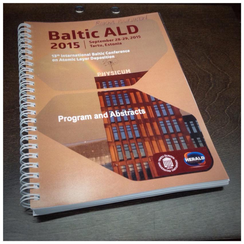
Book of abstracts (Riikka Puurunen, VTT, Twitter)
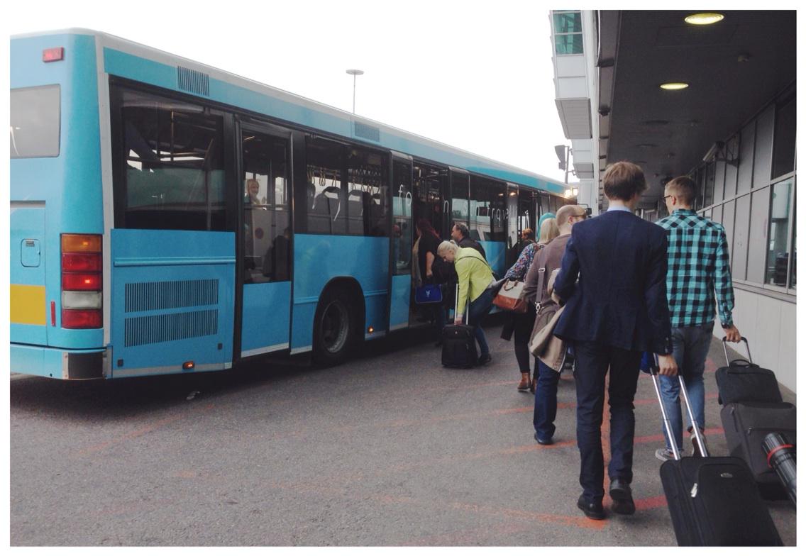
A bus load of ALD scientists from Helsinki heading for the Helsinki-Tartu flight. Last time (2002) they took the bus all the way to Tartu.
Tartu as viewed from the conference Hotel on Sunday afternoon (Irina Kärkkänen, Sentech)
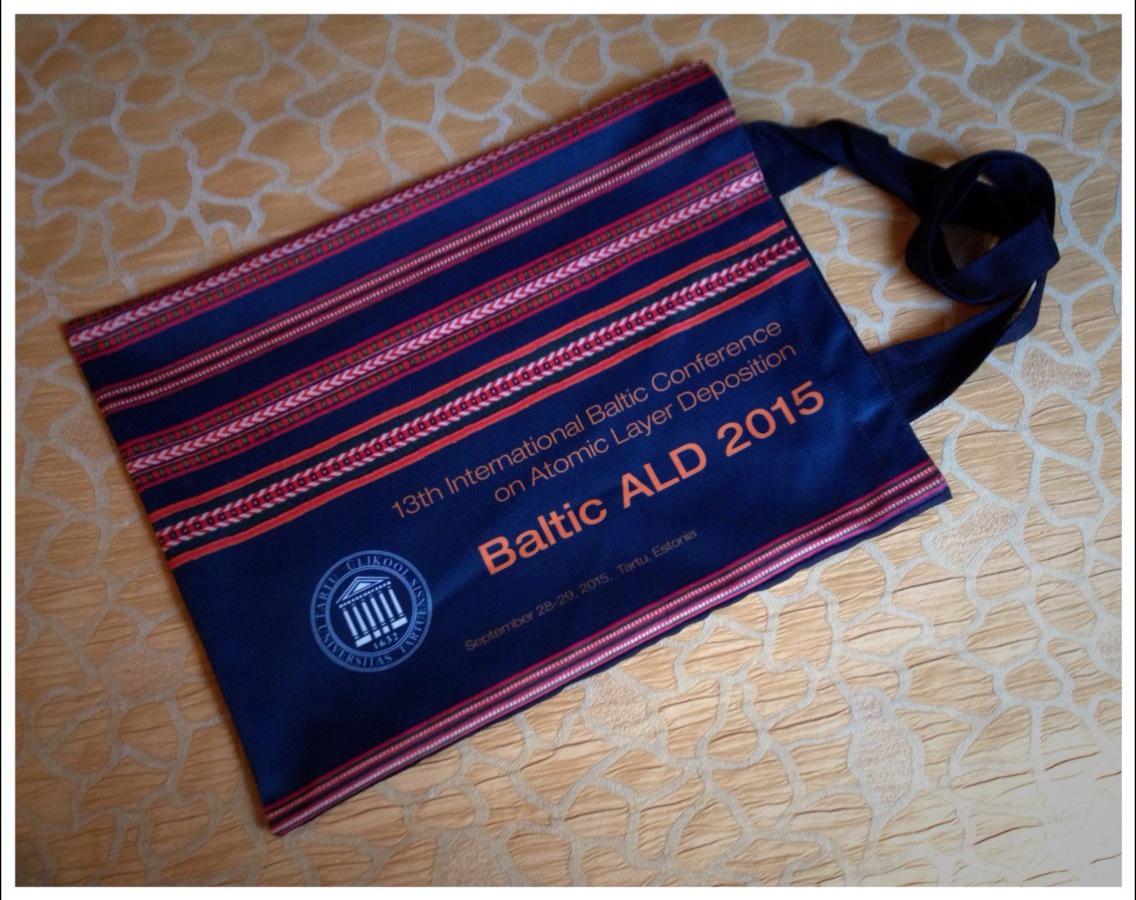
Conference bag - must be the best looking bag ever in the History of ALD (Riikka Puurunen, VTT, Twitter)
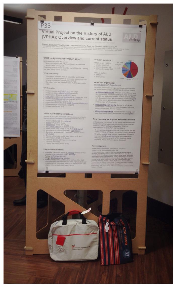
The Russian ALD bag next to the Estonian ALD Bag below the VPHA Poster (Riikka Puurunen, VTT, Twitter)
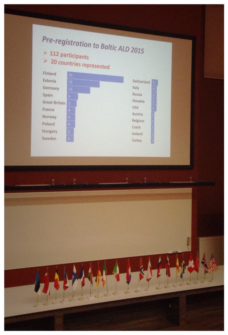
Participant distribution - Finland on top followed by Estonia and Germany (Riikka Puuronen, VTT, Twitter)
View at the podium (Simon Rushworth, EpiValance, LinkedIn)
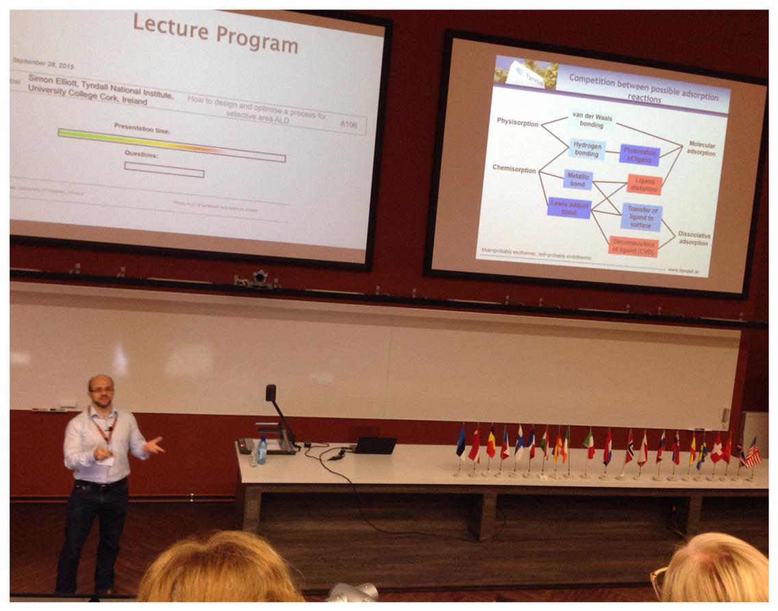
Modeling area-selective ALD, talk by Simon Elliott Tyndall (Riikka Puurunen, Twitter)
Timo Vähä-Ojala from Picosun talked about modelling of gas flow in ALD reactor (Tero Pilvi, Picosun)
Riikka Puurunen VTT - Mechanical property mapping of ALD thin films (Christoph Hossbach, TU-Dresden)
SOCIAL PROGRAM:
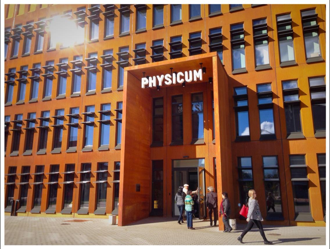
"Colours, colours! Physicum building at Tartu University" (Riikka Puurunen, VTT, Twitter)
Welcome Reception September 27, 2015
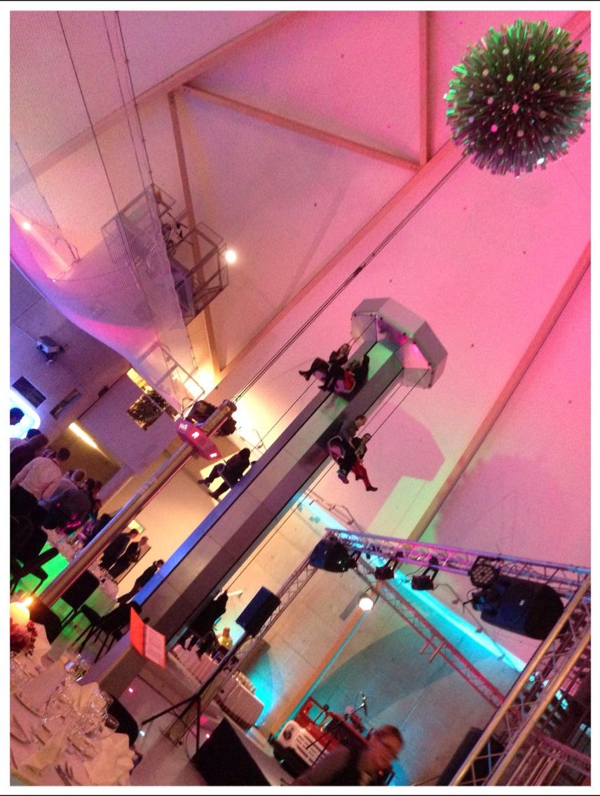
Conference Dinner September 28, 2015
"Conference dinner at AHHAA science centre was memorable with the pyro show, good food, music, and company" (Riikka Puurunen, VTT, Twitter)
Guided City Tours September, 29, 2015
SPONSORING
The conference venue showing the Exhibition area for a number of sponsoring companies: Armgate, Picosun, Oxford Instruments, Beneq, STREM Chemicals, SENTECH Instruments, Semilab, FAB Support.


%20(1).png)