Saturday, June 27, 2015

Photo show from AVS ALD 2015 in Portland

Here all pictures that appear on Twitter (#AVSALD2015) or that people send me (jonas.sundqvist@baldengineering.com) will be collected!


Impressions


Technical program and abstracts posted by Angel Yanguas-Gil on twitter


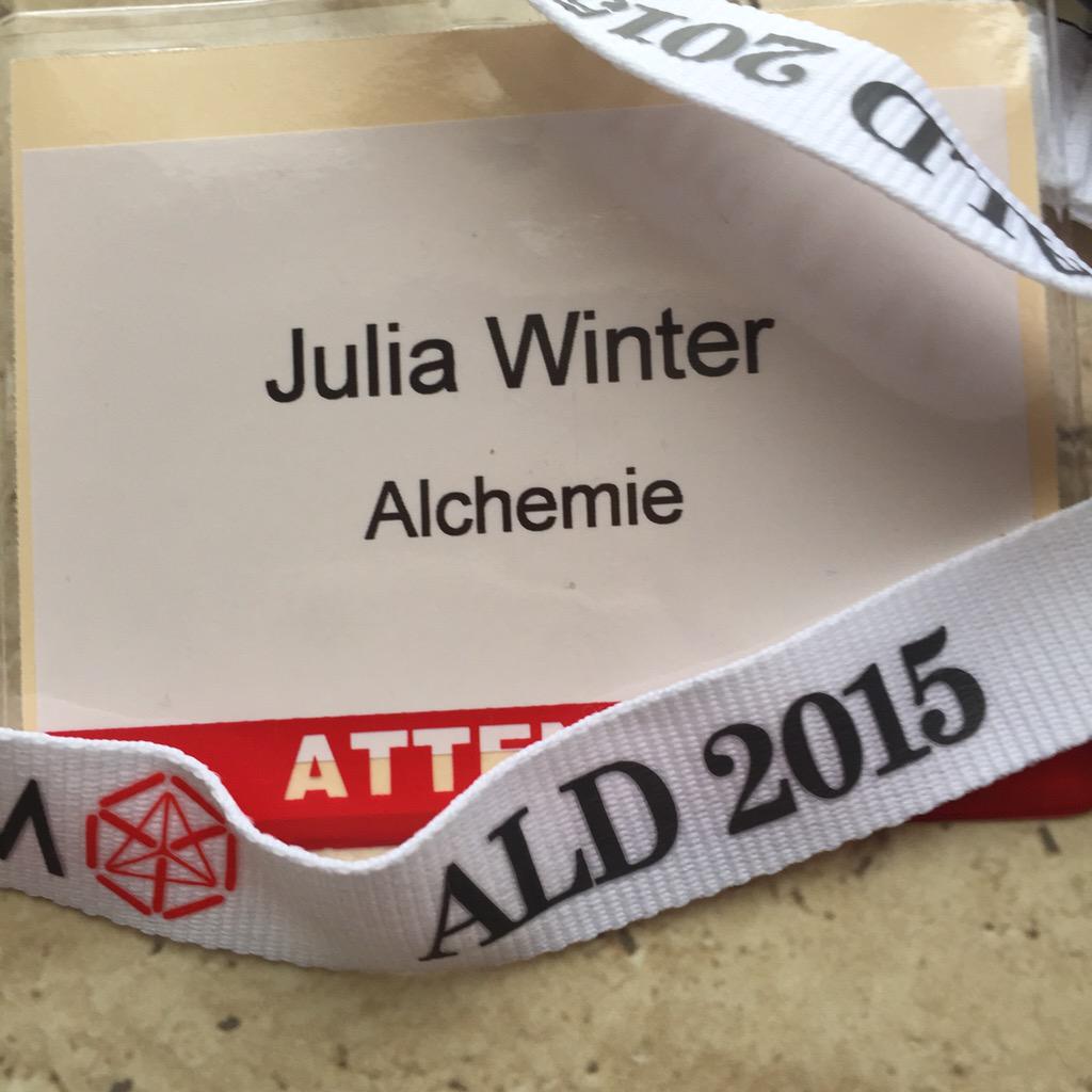
Julia Winter from http://www.alchem.ie gets her badge. Here you can also see that ASM has sponsored the key chain.

Seminars


Sunday Tutorials : Prof. Markku Leskelä, University of Helsinki, Finland, “ALD Process Development: Solutions to Industrial Challenges” Introduced by Prof. Winter. (Photo by Iain Buchanan)


Chuck Winter opens AVS ALD 2015. Over 750 attendees (!) and 400+ abstracts (Sean Barry, Twitter)


Here is a picture showing quite clear how broad ALD has become these days (Picture from Martin Knaut).

 
Another shot when the before the first pulse of ALD Experts has been injected (Sean Barry, Twitter)


ALD manufacturing session: packed room (Angel Yanguas-Gil, Twitter


Mato Knez giving a plenary on ALD Beyond Electronics (Sean Barry)


The Golden Boy getting ready for his and Canadas great Golden Day - Session B, 9:15: the first ever robust ALD Au metal process. (Sean Barry, Twitter))


Very good talk by Conley on MIIM diodes (Angel Yanguas-Gil, Twitter)


Poster sessions


Our poster on the evolution of ALD is now up! (Angel Yanguas-Gil, Twitter )


Vincent Vandalon wins the graduate student award for best presentation at #AVSALD2015! We are so proud! http://t.co/LU69IPAr4Q


ALD Trade show


The leading supplier of high quality Atomic Layer Deposition (ALD) technology for industrial manufacturing (Picture by Timo Malinen)


Pall Corporation showing their latest filter technology : Learn about precursor #filtration for contamination control in adv. #ALD processes (Twitter)


Pall Corporation Booth at the ALD trade show (Picture from Rob Nine)

EpiValence Booth http://www.epivalence.com (Picture form LinkedIn, Simon Rushworth)


Dinners and Receptions


Applied Materials, Picosun, Air Products and NSI sponsored party (Sean Barry, Twitter).


Applied Materials, Picosun, Air Products and NSI sponsored party (Martin Knaut, http://www.katharinaknaut.com)


Iain Buchanan from Air Products selling tones of high-k precursor (Martin Knaut, http://www.katharinaknaut.com)


Barking at the Moon (Martin Knaut, http://www.katharinaknaut.com)

Portland Sightseeing


Saturday by Sean Barry (from twitter)


The Golden Team from Ottawa Canada has arrived in Portland : These #BarryLab adventurers drove in a (crappy) van from @ottawacity to #AVSALD2015 in Portland. Check out the bumper


Air Products flying in to Portland passing Mount Hood (Iain Buchanan)


Mount Hood (Martin Knaut, http://www.katharinaknaut.com)


View from the hotel (Tero Pilvi)


Same as above later in the evening at one of the Parties. (Julia Winter, Twitter)


Portland view - Moon and Mountain (Tero Pilvi, Instagram)


The Moon rolling in heading for Mount Hood (Martin Knaut, http://www.katharinaknaut.com)


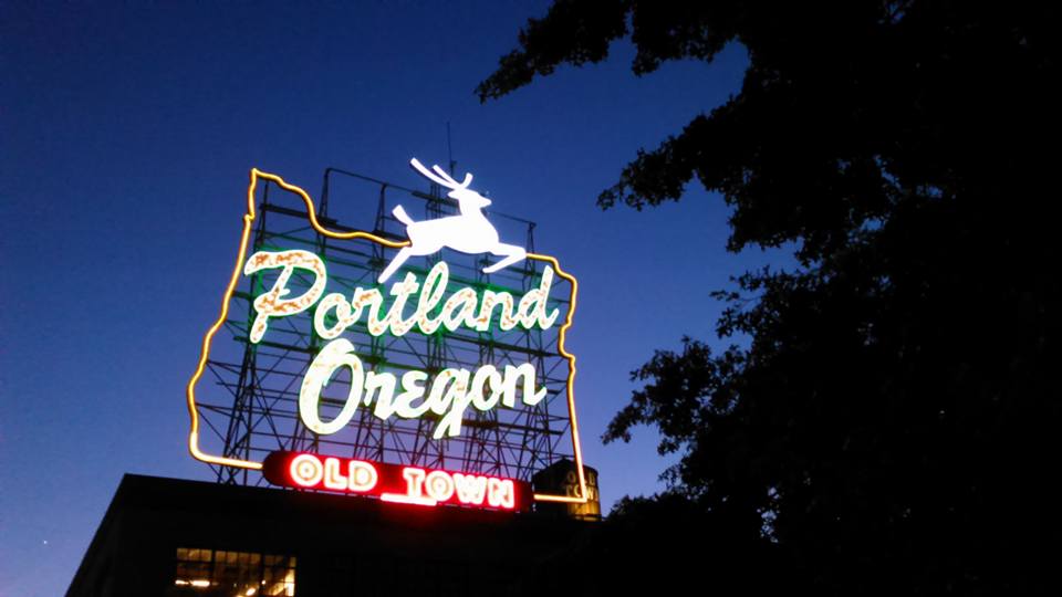
Old Town Chinatown is the official Chinatown of the Northwest section of Portland. The White Stag sign, a former advertising sign, greets those traveling into Old Town on the Burnside Bridge (Photo by Marcel Junige).


Portland sunset (Photo by Marcel Junige).


Portland airport with Mount Hood in the background (Photo by Marcel Junige).


ASM International Hosts ALD Technology Seminar in Portland at AVS ALD 2015

ASM International N.V. (NASDAQ: ASMI and Euronext Amsterdam: ASM) today announces that it will be hosting a technical seminar in Portland, OR, US, on Tuesday June 30, 2015, the second day of the ALD Conference.


In this 'All about ALD' technology seminar, ASM and a distinguished guest speaker will address challenges and opportunities for ALD processes and equipment to manufacture next generations of micro-electronic devices.

The agenda is as follows:

5.30 pm Reception, drinks and food 
6.15-6.30 pm Dr. ir. Ivo Raaijmakers (ASM) - Welcome and introduction
6.30-7.00 pm Dr. Jeffrey Elam (Argonne National Laboratory) - "Selective ALD in polymers: sequential
infiltration synthesis for lithography and nanofabrication " 
7.00-7.20 pm Dr. Suvi Haukka (ASM) - " Present and future challenges of atomic layer deposition"

Following the presentations, there is room for open discussion and networking until 9.00 pm.

The ASM technology seminar will take place in the Skyline room I-II at the Portland Hilton, 921 SW Sixth Ave., Portland, OR, 97204 US. The room will open at 5:30 pm for invited attendees. Interested parties should contact Rosanne de Vries, +31 88 100 8569, rosanne.de.vries@asm.com.


Friday, June 26, 2015

Beneq introduces a PEALD process to deposit silicon nitride on 3D structures with excellent uniformity


To yield superior thin film properties on planar as well as complex 3D structures, Beneq is now launching a highly competitive low-temperature, plasma-enhanced atomic layer deposition (PEALD) process for depositing silicon nitride (Si3N4).


The use of silicon nitride is extensive in many high-tech sectors, including the semiconductor industry, for micro-electromechanical systems (MEMS) and in medical applications. Silicon nitride thin films are ideal when used as chemical barriers and insulators in integrated circuits, or as diffusion barriers for microchips, or as dielectrics in capacitors.

Currently, CVD-based processes are largely used to grow silicon nitride (Si3N4) thin films. Due to the intrinsic mechanisms and properties of CVD processes, coating complex 3D structures with conformal and uniform thin films has been impossible. By introducing a robust and up-scalable Si3N4 process, Beneq is again paving the way for new opportunities in ALD.

The newly launched Beneq process now offers the opportunity to use Si3N4 in 3D structures in the semiconductor industry, for MEMS applications and much more. It features low processing temperatures, starting at 250 °C, for ease of production. The main specifications of the process are:
  • high uniformity on 3D structures
  • low temperature process – starting from 250 °C
  • Si3N4 thin film chemical composition
  • very low level of contaminants
  • safe to use – non-hazardous precursors
  • simple to upgrade – available for Beneq TFS 200 and TFS 500

“We’re really pleased to launch this unique Si3N4 depositing technology,” says Markus Bosund, Senior Scientist at Beneq. “Again, we can reach beyond the limitations of conventional thin film processes and offer a competitive ALD solution. Our PEALD process allows outstanding film properties for 3D structures at low temperatures. For Beneq, this is the next milestone in our history of bringing the world’s best ALD expertise to the market.” 

The process will be formally presented during ALD 2015, the 15th International Conference on Atomic Layer Deposition and main annual event for the global ALD community in research and industry. ALD 2015 will be held June 28th - July 1st, 2015, Portland, Oregon, USA, where Senior Scientist Markus Bosund will be presenting work that Beneq has completed together with Hewlett-Packard Co. and the University of Jyväskylä. The topic of his presentation is: “Saturation Behavior and Film Properties of Plasma-Enhanced ALD Grown Silicon Nitride”. 

Beneq is a pioneer in ALD equipment and applications development, with installed equipment serving university labs, research institutes and corporate R&D worldwide. Beneq is the developer of Roll-to-Roll ALD.

Research and Markets: 2015 ALD/CVD High K and Metal Precursors for the Semiconductor IC Market

Pretty impressive to know that "The semiconductor CVD/ALD industry utilizes precursors for over 29 different metals and metal oxides provided globally by 23 suppliers." Thanks Rob for sharing this one in the ALD LinkedIn Group!

Research and Markets has announced the addition of the "2015 ALD/CVD High K and Metal Precursors for the Semiconductor IC Market" report to their offering.

The High K / ALD Precursors report provides information on the applications and markets associated with front end and back end of line precursors used to produce high dielectric constant (K) dielectrics and atomic layer deposition dielectrics and metals. Market size, growth, and market share statistics are provided.

Rancho Santa Fe, CA, June 15: Use of front-end Ta and W metal gate and Hf gate dielectric precursors will grow over 2.5x by 2020, according to a new report from this research industry, 2015ALD/CVD High K and Metal Precursors for the Semiconductor IC Market. The overall precursor market sits at $185M today, and is expected to grow 18% over the next five years. The advanced metal gate and gate dielectric segments within that market are expected to grow at 168%, more than compensating for the 25% decline anticipated for the high memory precursor segment.

The 2014 market size for CVD/ALD precursors for interconnect applications was approximately $93M, up 19% over 2013. 2015 is forecast to be up another 15%. By 2016, growth in this segment will be dominated by cobalt barrier precursors, as WF for contact and plug applications begins to decline. The 5-year CAGR for this area is forecast to be 9.4% overall.

The precursor market for capacitor CVD/ALD applications, which includes DRAM and a variety of memory devices, is expected to be flat for the next 5 years, fluctuating in the range of $55M to $70M. The difficulties in forecasting conventional memory demand are compounded by the emergence of a host of new memory device structures, not all of which depend on these materials.

The semiconductor CVD/ALD industry utilizes precursors for over 29 different metals and metal oxides provided globally by 23 suppliers. In addition to market analysis, process flow details, precursor candidates and critical supply chain issues, the report includes regional ranking for major suppliers of vapor deposition precursors.

RASIRC to showcase technology leadership in hydrogen peroxide delivery in Portland

OMG it is heating up before the upcoming Atomic Layering weeks in Portland! RASIRC is well prepared. I know by own experience that they have the absolutely best technology there is for delivering hydrogen peroxide. It is sort of embarrassing after having worked and published papers on using a stander bubbler and realizing that I actually did not deliver basically any H2O2 onto the surface back then. Talk to Jeff Spiegelmann at the conferences he will explain it all for you.


RASIRC will showcase technology leadership in hydrogen peroxide gas for next generation semiconductor materials and processes with a poster session and exhibit (booth #39) at the 15th International Conference on Atomic Layer Deposition June 28-July 1 in Portland, Oregon. The company will present a second poster at the Atomic Layer Etching Workshop held immediately following the ALD Conference. The posters are titled “In-Situ Monitoring of Hydrogen Peroxide Vapor Delivery Systems for ALD” and “Novel Hydrogen Peroxide Delivery Systems for Atomic Layer Cleaning and Etch”.

“The ALD Conference and ALE Workshop are great forums for us to discuss our technology around hydrogen peroxide gas, which we believe will be a critical component in enabling next generation ALD and ALE processes,” said Jeffrey Spiegelman, RASIRC President and Founder. “Test results from in-situ monitoring clearly show that H2O2 gas delivery for ALD can be stable with or without water, and that H2O2 gas can remove carbon from ALD pre-initiation layers to eliminate wet cleaning steps.”

In-Situ Monitoring of H2O2 for ALD


H2O2 gas is more reactive with metal precursors than water and less aggressive than ozone. Process engineers can now deliver high concentration H2O2 gas to process with or without water. RASIRC co-developed an analyzer for in-situ monitoring of H2O2 gas to verify the H2O2 gas concentration flowing to process. Test results using the analyzer clearly show stable H2O2 gas concentration over extended periods of time. Tests were performed on both high concentration H2O2 gas delivery systems and anhydrous H2O2 gas delivery systems.

For high concentration systems using 30% H2O2 liquid source, tests showed stable delivery of up to 5% gas by volume. For anhydrous systems, test results showed stable, consistent delivery of virtually water-free H2O2 gas. Test results will be presented at a poster session on June 30 from 5:30pm-7:30pm.

H2O2 Gas for ALE


H2O2 gas for atomic layer etching enables process engineers to eliminate certain cleaning steps in processing next generation semiconductors. Uniform removal of layers is critical to device performance due to layers now being only several atoms thick, and H2O2 gas is ideally suited to this task. RASIRC will present test results showing that high concentration H2O2 gas can be generated and delivered to process at stable concentrations of up to 5% gas by volume. Preliminary test results with new materials and alternative chemistries will also be shown. The poster presentation will be on July 1 from 6:00pm-9:00pm.

ALD Conference Presence


For more information about H2O2 Gas with or without water, ALD Conference attendees are invited to visit RASIRC in booth #39. Representatives will be available to discuss technologies and test results.


CVD of vertically aligned silicon nanowires in MEMS using silane as a precursor

Here is a very good and detailed paper on CVD of vertically aligned silicon nanowires in MEMS using silane as a precursor by researchers at Catalonia Institute for Energy Research (IREC), Institute of Microelectronics of Barcelona, and ETH Zurich. Pretty high aspect ratio - Open Access - enjoy!

Towards a full integration of vertically aligned silicon nanowires in MEMS using silane as a precursor

G Gadea, A Morata, J D Santos, D Dávila, C Calaza, M Salleras, L Fonseca and A Tarancón
G Gadea et al 2015 Nanotechnology 26 195302


Samples with R = 168 and tdip = 30 s grown during 60 min at 32 mTorr of silane pressure (2.5 Torr total pressure) at different growth temperatures: (a) 520 °C; (b) 630 °C; (c) and (d) 725 °C ((d) shows a 20° tilted view). In (a), (b), and (c) higher-magnification insets show the nanowires at their middle section for diameter comparison. The inset in (d) shows a higher magnification of the nanowire tips from sample (c).

Abstract

Silicon nanowires present outstanding properties for electronics, energy, and environmental monitoring applications. However, their integration into microelectromechanical systems (MEMS) is a major issue so far due to low compatibility with mainstream technology, which complicates patterning and controlled morphology. This work addresses the growth of 〈111〉 aligned silicon nanowire arrays fully integrated into standard MEMS processing by means of the chemical vapor deposition–vapor liquid solid method (CVD–VLS) using silane as a precursor. A reinterpretation of the galvanic displacement method is presented for selectively depositing gold nanoparticles of controlled size and shape. Moreover, a comprehensive analysis of the effects of synthesis temperature and pressure on the growth rate and alignment of nanowires is presented for the most common silicon precursor, i.e., silane. Compared with previously reported protocols, the redefined galvanic displacement together with a silane-based CVD–VLS growth methodology provides a more standard and low-temperature (<650 °C) synthesis scheme and a compatible route to reliably grow Si nanowires in MEMS for advanced applications.

Thursday, June 25, 2015

Saxonian President Tillich propose Euro-Chip Foundry in Dresden


Sachsens Ministerpräsident Stanislaw Tillich. Abb.: J. Jeibmann/Staatskanzlei
The Minister-President of the German Free State of Saxony, Stanislaw Tillich (CDU) propose to the European Commission to build a European Foundry. Obviously he would like to see it built in Dresden.


Today two 300 mm Fabs are operated in Dresden, The Globalfoundries Fab1 running high performance CMOS down to 28 nm and having 22 nm FDSOI in pilot, according to a recent statement made in Grenoble (http://www.eetimes.com/document.asp?doc_id=1326954)

The other 300 mm Fab is the ex-Infineon, ex Qimonda - now Infineon 300 mm DRAM Fab that has been converted to manufacturing power semiconductors on 300mm thin wafers in its CoolMOS family. In addition, XFab has a 200 mm Fab in Dresden

It is not the first time this idea of a European foundry has surfaced in Dresden and it will be interesting to see at SEMICON Europa 6-8 October how serious this bold proposal by Mr. Tillich. We have to remember that it was on his watch when Infineon let Qimonda go down the drain in 2009. One point for discussion will obviously be - if Fab1 is struggling to keep i high utilization today - what products will fill the European Mega Fab. The answer can´t just be IoT and Industrie Vier-Punkt-Null - This would also be a Mega Investment! Let´s be hopeful - Go Tillich!


The Dresden manufacturing site is recognized throughout the industry as among the most successful leading-edge semiconductor production facility in the world. Fab 1 represents one of the biggest international investments in Germany with a total investment to date of more than $7 billion, and about 3,000 world-class engineers, technicians, and specialists. (www.globalfoundries.com)


The Dresden 200 mm site is characterized by a high degree of automation: Fully automated wafer transport, integrated production control and single wafer tracking are central elements. Every week thousands of silicon wafers pass through the highly complex production system in our high end clean room. Infineon Dresden runs production 24-hours a day, seven days a week throughout the year, in a modern and flexible shift system. In July 2011, the Infineon Management Board had decided to establish Dresden as the world's first high-volume production site for power semiconductor devices on 300mm wafers. (www.infineon.com)


The X-FAB Dresden location running analog/mixed-signal CMOS processes (www.xfab.com)

Ultratech-Cambridge NanoTech ships 400th ALD system

Ultratech, Inc., a supplier of lithography, laser­-processing and inspection systems used to manufacture semiconductor devices and high-­brightness LEDs (HB­-LEDs), as well as atomic layer deposition (ALD) systems, announced that its Cambridge NanoTech business unit, Ultratech-CNT, has shipped its 400th ALD system. The system was purchased by the University of Michigan.


Dr. Neil Dasgupta, Assistant Professor of Mechanical Engineering at University of Michigan, whose group received the ALD equipment, said, “Ultratech-CNT’s ALD system has provided a significant boost to our research productivity, enabling us to make rapid advances in the field of surface and interfacial modification of energy conversion devices, including batteries, solar cells, and catalysts. The versatility of the ALD system to address the varied needs of our research program, coupled with the depth of knowledge of their science and engineering team, has enabled us to move very quickly towards producing high-impact research. We are happy to be part of this significant milestone in receiving the 400th system, and we look forward to developing a strong relationship with Ultratech-CNT.”

Ultratech-CNT Vice-President of Research and Engineering, Ganesh Sundaram, Ph.D., said, “It has always been about the scientist and researcher, and about making them successful in achieving their research goals. We are extremely gratified by Professor Dasgupta’s decision to purchase our ALD system. We have known his work since his days as a graduate student at Stanford University, and he has consistently produced noteworthy results using ALD. Looking forward, we are excited by the prospects of the breakthroughs in science that he, along with all other researchers, will be making using our instruments. For our part, we celebrate the shipment of our 400th system and will continue our tradition of providing deep expertise combined with exciting technology.”

Ultratech-CNT’s ALD Systems: 


Savannah G2 ALD System

The Savannah G2 platform incorporates a wide range of advanced field-upgradable options intended to aid serious researchers in expanding their portfolio of available ALD films, as well as allow them to characterize the films in real time.


Phoenix G2 Batch ALD System

Engineered for high throughput, the Phoenix provides maximum uptime in any fabrication environment from pilot production to industrial-grade manufacturing. Technologists and researchers rely on the Phoenix for repeatable, highly-accurate film deposition on flat and 3-D substrates alike for batch production ALD requirements.


Fiji High-Vacuum ALD System

A modular, high-vacuum ALD system, the Fiji series accommodates a wide range of deposition modes using a flexible architecture and multiple configurations of precursors and plasma gases. The result is a next-generation ALD system capable of performing thermal and plasma-enhanced deposition.


Wednesday, June 24, 2015

Imec expands strategic partnership with Toshiba and SanDisk

Nanoelectronics research center imec, announced today at the Imec Technology Forum 2015 (Brussels) that Toshiba Corporation (Tokyo: 6502), SanDisk Corporation (NASDAQ: SNDK) and imec have expanded their strategic partnership with Toshiba and SanDisk joining imec’s industrial affiliation program on advanced patterning. This program tackles the critical challenges that remain in bringing EUVL to high volume manufacturing. The program also develops other technologies for extending 193nm immersion lithography. Toshiba and SanDisk have been core partners in imec’s industrial affiliation program in Advanced Memory since 2011. 


“This expanded agreement with Toshiba and SanDisk represents the next step in our long-term strategic and fruitful partnership. We are proud to join forces and strengthen our collective research competence in advanced patterning,” said Luc Van den hove, President and CEO at imec. “The agreement is a testament of the industrial value and impact our R&D programs have on advanced semiconductor scaling. To date, this program, supported by our world-class infrastructure, represents the largest investment in advanced lithography equipment in the world.” 


“Our participation in imec’s advanced patterning program provides us access to state-of-the-art lithography infrastructure for EUV technology R&D,” said Dr. Ritu Shrivastava, Vice President, Technology Development, SanDisk. “We look forward to contributing to expanding the knowledge base in this important field.”

“We are pleased to be expanding our successful strategic partnership with imec,” said Susumu Yoshikawa, Technology Executive, Memory Technology of Semiconductor & Storage Products Company, Toshiba Corporation. “This leading-edge lithography technology program should be an important contributor to accelerating scale-up in high volume semiconductor manufacturing.”

Imec’s research into advanced patterning includes GLOBALFOUNDRIES, INTEL, Micron, Panasonic, Samsung, SK Hynix, Sony, Toshiba/SanDisk and TSMC.

Tuesday, June 23, 2015

Chinese Labs produce Ultraclean and large-area monolayer hexagonal boron nitride on Cu foil by LPCVD

Researchers from The National Center for Nanoscience and Technology and Hubei University People's Republic of China has presented result on synthesis of large-area (4 × 2 cm2) high quality monolayer h-BN with an ultraclean and unbroken surface on copper foil by using LPCVD.


Monolayer h-BN, SAED diffraction and h-BN on SiO2/Si substrate (Source : http://nanotechweb.org/cws/article/lab/61589).

Ultraclean and large-area monolayer hexagonal boron nitride on Cu foil using chemical vapor deposition

Yao Wen, Xunzhong Shang, Ji Dong, Kai Xu, Jun He and Chao Jiang
2015 Nanotechnology 26 275601. doi:10.1088/0957-4484/26/27/275601

Atomically thin hexagonal boron nitride (h-BN) has been demonstrated to be an excellent dielectric layer as well as an ideal van der Waals epitaxial substrate for fabrication of two-dimensional (2D) atomic layers and their vertical heterostructures. Although many groups have obtained large-scale monolayer h-BN through low pressure chemical vapor deposition (LPCVD), it is still a challenge to grow clean monolayers without the reduction of domain size. Here we report the synthesis of large-area (4 × 2 cm2) high quality monolayer h-BN with an ultraclean and unbroken surface on copper foil by using LPCVD. A detailed investigation of the key factors affecting growth and transfer of the monolayer was carried out in order to eliminate the adverse effects of impurity particles. Furthermore, an optimized transfer approach allowed the nondestructive and clean transfer of the monolayer from copper foil onto an arbitrary substrate, including a flexible substrate, under mild conditions. Atomic force microscopy indicated that the root-mean-square (RMS) roughness of the monolayer h-BN on SiO2 was less than 0.269 nm for areas with fewer wrinkles. Selective area electron diffraction analysis of the h-BN revealed a pattern of hexagonal diffraction spots, which unambiguously demonstrated its highly crystalline character. Our work paves the way toward the use of ultraclean and large-area monolayer h-BN as the dielectric layer in the fabrication of high performance electronic and optoelectronic devices for novel 2D atomic layer materials.

Picosun and Nanexa collaborate in ALD for Medical technology in ECSEL InForMed led by Philips

Picosun Oy provides the advanced ALD coating solutions to enable the next generation of cutting-edge medical technology.


ALD’s unique ability to form perfectly hermetic but still ultra-thin encapsulation layers to cover even the smallest, most complex surface details and particles is an invaluable asset to the medical equipment and medicine manufacturers. It increases the operational life, reliability, and safety of the equipment and enables advanced synthesis, delivery, and dosing of medical substances. Several ALDmaterials are naturally biocompatible and, as a gas-phase, low temperature method, ALD allows coating of sensitive substrates such as plastics and polymers – key materials in various medical devices.


“Incorporation of our ALD solutions into the field of medical technology opens up an interesting new market for us. ALD-enabled medical innovations already create growth and success for our customers – an example being recently stock listed Nanexa AB in Sweden, which utilizes our ALD technology in production of nanofabricated drug delivery Systems. In InForMed, one of our new, inter-European ECSEL projects we cooperate with the leading industries in the field. We are excited to see our ALDexpertise realize the most advanced, better, safer, and patient-friendly diagnostics and treatment equipment,” states Juhana Kostamo, Managing Director of Picosun.

Source: PrNewsWire
Picosun ALD Breaks Through in Medical Technology

The InForMed project - ECSEL Joint Undertaking


The project InForMed (An integrated pilot line for micro-fabricated medical devices), running from 1st June 2015 to 31st May 2018 is financed by ECSEL Joint Undertaking.

The InForMed project will establish an industrial integrated micro-fabrication pilot line for medical devices, covering the complete innovation chain from technology concept to system qualification.

The heart of the pilot line is the industrial facility of Philips Innovation Services (PInS), which will serve as a small/medium-scale production and assembly facility, qualified for medical devices. Connected to this infrastructure are European partners who provide complementary capabilities that enable the heterogeneous integration required for these devices.

The pilot line is fed by new concepts, generated by academic and industrial research. For high volume production the pilot line is connected to well established foundries. Protocols have been defined to ensure an efficient transfer of technologies from the concept creation phase (TRL 4/5) to the pilot line, and from the pilot line to high volumes production (TRL 7/8).

The pilot line is demonstrated by six demonstrator products that cover innovations in existing markets, enable emerging markets and pioneer new markets, respectively. The pilot line will help consolidating Europe’s strong position in diagnostic equipment, and it will create innovative value chains in emerging and new markets in medical equipment and even pharmacology.

Monday, June 22, 2015

Pegasus - New UK ALD and CVD Precursor company


Pegasus Chemicals is a privately owned UK company focused on localised support of the European ALD and CVD community with our ability to supply specialist chemicals, packaged for individual applications. We specialise in the high purity transfil and manufacture of small scale products for niche applications. Our product portfolio is wide and varied with specific focus on intrinsic purity and consistency. Our technical and product application knowledge in ALD and CVD has been honed through the manufacture and supply of specialist chemistry with many years experience. Our technical service team is available to discuss your deposition requirements to tailor the product with the application. 

www.pegasuschemicals.com 

Penn State - Diode a few atoms thick shows surprising quantum effect

As publish by Penn State : A quantum mechanical transport phenomenon demonstrated for the first time in synthetic, atomically-thin layered material at room temperature could lead to novel nanoelectronic circuits and devices, according to researchers at Penn State and three other U.S. and international universities.


Atomic multilayer structure of van der Waals solids representing layering with a graphene substrate.


Current-voltage curves of single junction (green) van der Waals solid (no NDR) and multijunction (red, orange) van der Waals solids (NDR). Stacking and choice of materials determines the location and width of peak.

The quantum transport effect, called negative differential resistance (NDR), was observed when a voltage was applied to structures made of one-atom-thick layers of several layered materials known as van der Waals materials. The three-part structures consist of a base of graphene followed by atomic layers of either molybdenum disulfide (MoS2), molybdenum diselenide (MoSe2), or tungsten diselenide (WSe2).

NDR is a phenomenon in which the wave nature of electrons allows them to tunnel through any material with varying resistance. The potential of NDR lies in low voltage electronic circuits that could be operated at high frequency.

“Theory suggests that stacking two-dimensional layers of different materials one atop the other can lead to new materials with new phenomena,” said Joshua Robinson, a Penn State assistant professor of materials science and engineering whose student, Yu-Chuan Lin, is first author on a paper appearing online today, June 19, in the journal Nature Communications. The paper is titled “Atomically Thin Resonant Tunnel Diodes Built from Synthetic van der Waals Heterostructures.”

Achieving NDR in a resonant tunneling diode at room temperature requires nearly perfect interfaces, which are possible using direct growth techniques, in this case oxide vaporization of molybdenum oxide in the presence of sulfur vapor to make the MoS2 layer, and metal organic chemical vapor deposition to make the WSe2 and MoSe2.

Sunday, June 21, 2015

A Novel ALD SiBCN Low-k Spacer for FinFETs presented at VLSI 2015 in Kyoto


A key challenge in reducing capacitance around the transistor is incorporating spacer and contact etch stop materials that are simultaneously low-k and robust to processing. One approach is to develop new low-k materials that can withstand the processing conditions [IEEE TRANSACTIONS ON ELECTRON DEVICES, VOL. 59, NO. 7, JULY 2012]


A Novel ALD SiBCN Low-k Spacer for FinFETs presented at VLSI 2015 in Kyoto by IBM and Globalfoundries. The abstract does not give too many details on the ALD process itself except that it is a "a novel low temperature ALD-based SiBCN material has been identified". However, the conference proceeding states that the SiBCN is deposited in a batch furnace:
  • SiBCN low k spacer was deposited in a batch furnace at 600 °C. The referral to low thermal process here may relate to earlier CVD processes at higher process temperatures.
  • The process was run in thermal ALD mode with alternating layers of BN and SiCN. 
  • The B/C ratio in the film was controlled by adjusting the BN:SiCN cycle ratio

A Novel ALD SiBCN Low-k Spacer for Parasitic Capacitance Reduction in FinFETs

T. Yamashita*, S. Mehta*, V. S. Basker*, R. Southwick*, A. Kumar**, R. Kambhampati*** , R. Sathiyanarayanan**, J. Johnson**, T. Hook*, S. Cohen*, J. Li*, A. Madan*, Z. Zhu*, L. Tai*, Y. Yao*, P. Chinthamanipeta*, M. Hopstaken*, Z. Liu*, D. Lu*, F. Chen**, S. Khan**, D. Canaperi*, B. Haran*, J. Stathis*, P. Oldiges*, C.-H. Lin*, S. Narasimha**, A. Bryant*, W. K. Henson**, S. Kanakasabapathy*, K. V. R. M. Murali**, T. Gow*, D. McHerron*, H. Bu* and M. Khare*, *IBM Research, **IBM SRDC and ***GLOBALFOUNDRIES, USA 

FinFET has become the mainstream logic device architecture in recent technology nodes due to its superior electrostatic and leakage control. However, parasitic capacitance has been a key performance detractor in 3D FinFETs. In this work, a novel low temperature ALD-based SiBCN material has been identified, with an optimized spacer RIE process developed to preserve the low-k value and provide compatibility with the down-stream processes. The material has been integrated into a manufacturable 14nm replacement-metal-gate (RMG) FinFET baseline with a demonstrated ~8% performance improvement in the RO delay with reliability meeting the technology requirement. A guideline for spacer design consideration for 10nm node and beyond is also provided based on the comprehensive material properties and reliability evaluations.

Friday, June 19, 2015

How to make carbon nano particles in the kitchen

Stuff the naked chef Jamie Oliver - Welcome to the first season of The Bald Swedish Chef - humpee, dumpee dump - put the chicken in the pot. In our first show we will take a closer look on how you can make car con nano particles at home in your kitchen.


Some background information - why do we need nano sized carbon particles in the first case? As reported here in Science Daily, researchers have found an easy way to produce carbon nanoparticles that are small enough to evade the body's immune system, reflect light in the near-infrared range for easy detection, and carry payloads of pharmaceutical drugs to targeted tissues. 


University of Illinois postdoctoral researcher Prabuddha Mukherjee, left, bioengineering professors Rohit Bhargava and Dipanjan Pan, and postdoctoral researcher Santosh Misra, right, report the development of a new class of carbon nanoparticles for biomedical use.

The researchers form Illinois at Urbana-Champaign have developed a new approach that generates the particles in a few hours and uses only a handful of ingredients, including store-bought molasses.

"If you have a microwave and honey or molasses, you can pretty much make these particles at home," Pan said. "You just mix them together and cook it for a few minutes, and you get something that looks like char, but that is nanoparticles with high luminescence. This is one of the simplest systems that we can think of. It is safe and highly scalable for eventual clinical use."

The nanoparticles also can be made quite small, less than eight nanometers in diameter.

"Our immune system fails to recognize anything under 10 nanometers," Pan said. "So, these tiny particles are kind of camouflaged, I would say; they are hiding from the human immune system."

So guys, I am off on a camping trip to South of France and if I come across any of that grandma´s Molasses at Carrefour I intend to report back on the experimental procedure. Stay tuned. I did however forget to pack the TEM grids so the verification of the results have to wait until I am back in the lab. Unless there is an optical scattering method that can be used to detect those particles...

The abstract to the paper where the research above has been reported:

Tunable Luminescent Carbon Nanospheres with Well-Defined Nanoscale Chemistry for Synchronized Imaging and Therapy


Prabuddha Mukherjee, Santosh K. Misra, Mark C. Gryka, Huei-Huei Chang, Saumya Tiwari, William L. Wilson,  John W. Scott, Rohit Bhargava and Dipanjan Pan
Article first published online: 20 MAY 2015

In this work, we demonstrate the significance of defined surface chemistry in synthesizing luminescent carbon nanomaterials (LCN) with the capability to perform dual functions (i.e., diagnostic imaging and therapy). The surface chemistry of LCN has been tailored to achieve two different varieties: one that has a thermoresponsive polymer and aids in the controlled delivery of drugs, and the other that has fluorescence emission both in the visible and near-infrared (NIR) region and can be explored for advanced diagnostic modes. Although these particles are synthesized using simple, yet scalable hydrothermal methods, they exhibit remarkable stability, photoluminescence and biocompatibility. The photoluminescence properties of these materials are tunable through careful choice of surface-passivating agents and can be exploited for both visible and NIR imaging. Here the synthetic strategy demonstrates the possibility to incorporate a potent antimetastatic agent for inhibiting melanomas in vitro. Since both particles are Raman active, their dispersion on skin surface is reported with Raman imaging and utilizing photoluminescence, their depth penetration is analysed using fluorescence 3D imaging. Our results indicate a new generation of tunable carbon-based probes for diagnosis, therapy or both.