Wednesday, June 7, 2017

Another breakthrough in CMOS-compatible ferroelectric memory

Imec, the world-leading research and innovation hub in nanoelectronics and digital technology, announced today at the 2017 Symposia on VLSI Technology and Circuits the world's first demonstration of a vertically stacked ferroelectric Al doped HfO2 device for NAND applications. Using a new material and a novel architecture, imec has created a non-volatile memory concept with attractive characteristics for power consumption, switching speed, scalability and retention. The achievement shows that ferro-electric memory is a highly promising technology at various points in the memory hierarchy, and as a new technology for storage class memory. Imec will further develop the concept in collaboration with the world's leading producers of memory ICs.

Full story : LINK

Monday, June 5, 2017

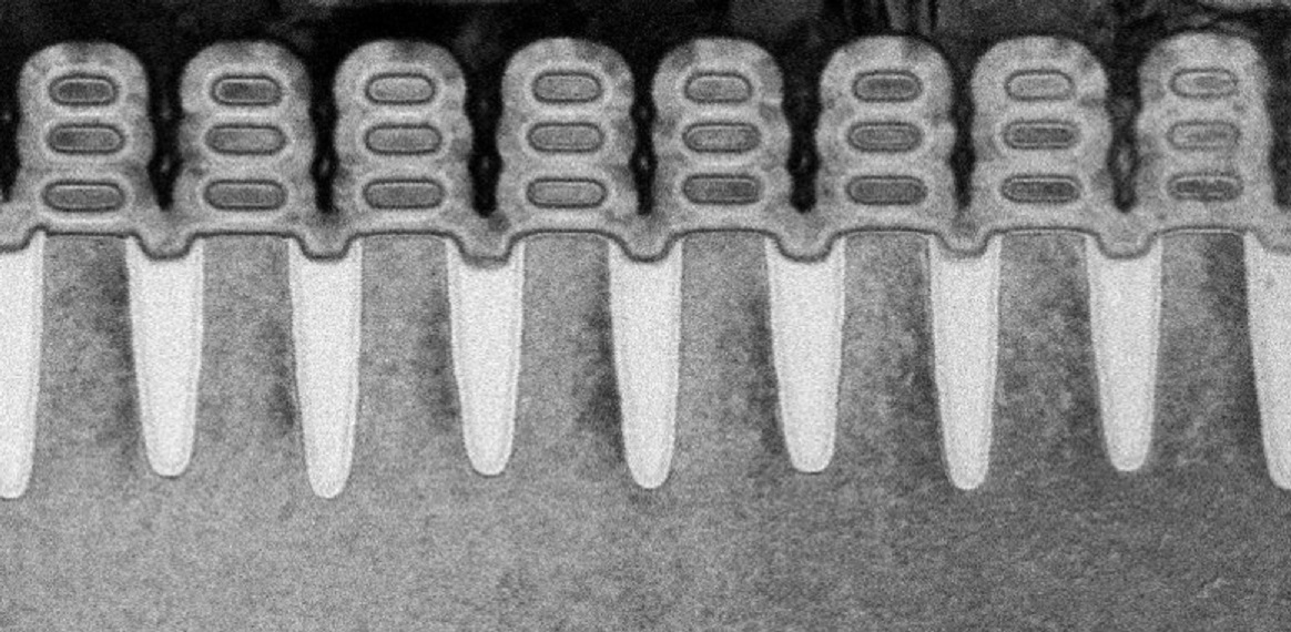
IBM, Samsung and Globalfoundries shows off the world´s first 5 nm logic chip with GAAFETs

IBM together with Samsung and Globalfoundries shows off the world´s first 5 nm logic chip with horizontal Gate All Around Field Effect Transistors also referred to as GAAFETs. GAAFETs are a evolutionary development out of FInFETS that were fisrt introduced at 22 nm by Intel. It is predicted that 7 nm will be the last FinFET node and that GAAFETs has to be introduced by then.

Source: IBM LINK

 TEM cross section of 5nm GAAFETs by IBM, Samsung and Globalfoundries (Source IBM)

The GAAFETs are manufactued by deposition stacks of epitaxial silicon and silicon germanium (Si/SiGe Epi). Then by using a combination of EUV lithography and reportedly (LINK) Atomic Layer Etching (ALE) trenches are etched to separate the stack into fins and then afterwards to individual nanowires (or nano sheets as IBM calls them) of Si resp SiGe forming the channels stacked on top of each other. Later the high-k / metal gate (HKMG) stack is deposited in by a sequence of ALD processes conformally covering the nanowire channels.


In the nano sheet FETs, the wires are much wider and thicker presumably giving the nano sheet FETs better electrostatics and drive current

Articles :

Want a smarter phone? IBM and Samsung bring you: Nanosheets!
CNET
If you're frustrated with smartwatches that aren't that smart or phones that don't pack enough power, IBM and Samsung have some good news ...


Sunday, June 4, 2017

EpiValence is sposnoring Best Student Awards at EuroCVD-Baltic ALD 2017 in Sweden

I just a week the EuroCVD-Baltic ALD 2017 conference kicks off in Linköping, Sweden (11-14th of June). Right now many students are putting their final touches to their presentations and posters and to motivate you even more we have a treat for you!


Epivalence is sponsoring the best student poster and best student presentation prices, which will be given at the conference dinner. You can meet Equivalence in the Industry exhibition at the conference.

Thursday, June 1, 2017

Pushing the Bounds of Nanoscale Processing at 'Nanotech 2017: Pushing the Limits' Workshop

Oxford Instruments and the Kavli Nanoscience Institute at the California Institute of Technology (CALTECH) are holding a one day workshop on 19th July 2017.

This workshop will explore recent progress in nanoscale plasma processing research and development, plus looking at future trends in the fabrication and application of micro, nano and atomic scale structures and devices.

Source: AZoNano LINK


Wednesday, May 31, 2017

Extended Deadline for Abstracts E-MRS 2017 Fall Meeting

E-MRS 2017 Fall Meeting Final Call [PDF] About E-MRS Contact
E-MRS 2017 Fall Meeting
Extended Deadline for Abstracts
The 2017 E-MRS Fall Meeting and Exhibit will be held
in Warsaw University of Technology
from September 18th to 21st - Monday-Thursday
The conference will include 23 parallel symposia,
one plenary session, one exhibition
and much more;
New Abstract deadline: June 5th, 2017

ALD barrier improves stability of perovskite quantum dots

EPFL Reports: A new approach to stabilize perovskite quantum dots has been developed in the lab of Raffaella Buonsanti at EPFL Valais Wallis. ALD was used to encapsulate the perovskite quantum dots with an amorphous alumina matrix, which acts as a gas and ion diffusion barrier making the quantum dots more robust against air, light, heat, and moisture.


Reference paper: A. Loiudice, S. Saris, E. Oveisi, D. T. L. Alexander, R. Buonsanti. CsPbBr3 QD/AlOx inorganic nanocomposites with exceptional stability in water, light and heat. Angewandte Chemie 26 May 2017. DOI: 10.1002/anie.201703703

According to the publication an Ultratech/CNT Savannah 200 ALD was used to process the Al2O3 barrier. Please fin all the details in the supporting information (LINK) as well as a movie showing the accelerated test in a water bath (LINK)

Tuesday, May 30, 2017

The AVS ALD2017/ALE2017 schedule and book of abstracts is now available online

The AVS ALD2017/ALE2017 schedule and book of abstracts is now available online & technical program:  


The AVS 17th International Conference on Atomic Layer Deposition (ALD 2017) featuring the 4th International Atomic Layer Etching Workshop (ALE 2017)  will be a three-day meeting dedicated to the science and technology of atomic layer controlled deposition of thin films and now topics related to atomic layer etching. Since 2001, the ALD conference has been held alternately in the United States, Europe and Asia, allowing fruitful exchange of ideas, know-how and practices between scientists. This year, the ALD conference will again incorporate the Atomic Layer Etching 2017 Workshop (ALE 2017), so that attendees can interact freely. The conference will take place Saturday, July 15-Tuesday, July 18, 2017, at the Sheraton Downtown Denver in Denver, Colorado, USA. 

Monday, May 29, 2017

Picosun reports repeat sales of production cluster systems

ESPOO, Finland, 29th May, 2017 – Picosun Oy, leading supplier of advanced Atomic Layer Deposition (ALD) thin film coating technology, reports of repeat sales of PICOPLATFORM™ production cluster systems to major industries.

The PICOPLATFORM™ cluster systems are designed for fully automated, high throughput operation in production environment. Several leading microelectronics manufacturers in USA and Asia have chosen these systems to manufacture IC components in the most advanced semiconductor nodes. The SEMI S2/S8 compatible PICOPLATFORM™ systems can handle wafers up to 300 mm size. The modular configuration with a comprehensive variety of wafer handling automation systems ensures each PICOPLATFORM™ cluster can be tailored for optimal performance according to each customer’s individual needs, whereas fast processing ensures low cost of ownership. To maximize system uptime and to guarantee always flawless process quality, Picosun provides all-inclusive after sales support, including precursor delivery services, through PicoSupport™ and PicoDevelopment™ service contracts and programs.

“We are proud of the confidence that our industrial customers place on us. Today, we collaborate with the global tier one businesses in semiconductor manufacturing. These companies are leaders in their own fields and possess the highest expertise in what they do, but when it comes to ALD, it’s Picosun in whom they trust. Repeated sales of production cluster systems to these companies proves our ability to satisfy even the most stringent demands of semiconductor industry leaders,” states Mr. Kustaa Poutiainen, Chairman of the Board and Chief Executive Officer of Picosun.

Saturday, May 27, 2017

Argonne scientists uses ALD vanadium as a catalyst for hydrogenation

Argonne researcher Max Delferro enhanced a process for catalytic activity of  vanadium for hydrogenation. The advantage is that if we can make vanadium that is an abundant metal catalytically active there are huge cost savings compared to using noble metals like Platinum or Paladium.

“Getting single-atom vanadium into this special configuration on metal oxide surfaces is not easy,” Delferro said. “It requires the use of special synthetic techniques such as surface organometallic chemistry and atomic layer deposition. However, if we can make vanadium or another abundant metal as catalytically active as the noble metals, we can create dramatic cost savings in these very common and commercially important catalytic processes.” Delferro said in a press release by Argonne (LINK).


Check out the new branding of Picosun - Agile ALD Solutions

Check out the new branding of Picosun - Agile ALD Solutions! (LINK)


You can meet Picosun exhibiting on the follwing upcming events:

June 11 - 14 Linköping, Sweden
EuroCVD-21 – BalticALD-15 

July 11 - 13 San Francisco, CA, USA
Semicon West 2017 (booth # 7121) 

July 15 - 18 Denver, CO, USA
ALD 2017 – The 17th International Conference on Atomic Layer Deposition (booth # 8-9) 

September 13 - 15 Taipei, Taiwan
Semicon Taiwan 2017

Veeco Completes Acquisition of Ultratech

Thin-film etch and deposition process equipment maker Veeco Instruments Inc of Plainview, NY, USA has completed its acquisition of Ultratech Inc of San Jose, CA, USA (which designs and makes lithography, laser-processing and inspection systems used to manufacture semiconductor devices and LEDs...


Source: Semiconductor Today
Read full article >

Friday, May 26, 2017

ALD & Synchotron Radiation at e-MRS 2017, fall meeting in Warsaw

Information from the symposium chairs Malgorzata Kot, Claudia Wiemer, Gianluca Ciatto and Joachim Schnadt: The deadline for abstract submission to e-MRS 2017, fall meeting, is approaching, please consider to submit an abstract to:

SYMPOSIUM Q: "SYNCHROTRON RADIATION AND ATOMIC LAYER DEPOSITION FOR ADVANCED MATERIALS"

Please visit the symposium website at
http://www.european-mrs.com/synchrotron-radiation-and-atomic-layer-deposition-advanced-materials-emrs

abstract submission deadline: Monday, May 29th!

Hot topics to be covered by the symposium:
  • Characterization of ALD processes and materials (metals, oxides) using synchrotron light (PES, XANES, EXAFS, GISAXS, XRD, XRR, XRF, etc.)
  • Investigation of ALD film nucleation, interface properties and growth by laboratory-based tools
  • In situ/operando monitoring of ALD processes (APXPS, infrared spectroscopy, etc.)
  • Modeling of the Atomic Layer Deposition
  • ALD method types (thermal, plasma and electron enhanced, spatial, etc.) 
  • Application of ALD (solar cells, LED, HEMT, MIM capacitors, LMR silica-fiber sensors, GaN power devices, TSV field effect transistor, MEMS, etc.)


Aixtron to sell its ALD/CVD business to Eugene Technology


Aixtron will sell the ALD and CVD memory product line, at Aixtron, Inc. based in Sunnyvale, California to Eugene Technology Inc., a wholly owned U.S. subsidiary of Eugene Technology Co., Ltd, South Korea.

Source: Evertiq
Read full article >

Aixtron completed take over of American ALD/CVD rival Genus, Inc. in March 2005 for about USD 140 million. This deal is reported to be in the order of USD 45 million and 55 million, which is considerably less.

Reportedly, the main customer today for Aixtron ALD is Samsung and the Aixtron ALD/CVD semiconductor business unit has had an annual revenue at about USD 20 to 40 million the last years years.


Thursday, May 25, 2017

International Training School on Atomic Layer Deposition - ALD-UKRAINE 2017

At this training workshop, top class experts from top research laboratories around the world will share their knowledge and experience in ALD, reviewing the current trends for R&D organizations.
Atomic layer deposition (ALD) – is a unique technique that allows to develop and implement numerous emerging technologies in such fields as: micro-nano(opto) electronics, flexible electronics, anti-corrosion surfaces, biocompatible coatings for biomedical applications, textiles, implantology, self-cleaning coatings, etc. Since Ukraine is represented in all these fields, ALD-UKRAINE 2017 is a beneficial event for research and industrial community that can lead Ukrainian R&D institutes and enterprises to a new level of development.


The event is organized by the HERALD COST Action and the Institute of Microdevices (NAS of Ukraine) in collaboration with Igor Sikorsky Kyiv Polytechnic Institute and IEEE Ukraine Section. For more information please check out the event website
Dates: 30 May 2017 to 1 Jun 2017 

Organising Members:
Simon Elliott
Petro Deminskyi

Samsung Display Unveil World’s First ‘Stretchable’ OLED Panel

Business Korea reports: Samsung Display announced on May 22 that it will showcase its advanced future display products which have never been revealed such as stretchable display, glasses-free 3D organic light-emitting diode (OLED) and ultra-high-definition LCD display that features 2,250 pixels per inch (ppi), at the Society for Information Display (SID) 2017, which will be held at the Los Angeles Convention Center from May 23 to 25 (local time).


The most striking exhibit from Samsung at the event will be a 9.1-inch stretchable OLED display. The product is a next generation display technology that can be flexibly stretched. It is considered the future technology that fits the most for wearable, Internet of Things (IoT) and artificial intelligence (AI) devices as well as automotive displays.

Full story:  LINK

Updated website PillarHall for ALD conformality test structures

Updated website PillarHall for ALD conformality test structures : http://www.pillarhall.com


MV Products' Vacuum Inlet Traps Protect Atomic Layer Deposition Tools

North Billerica, MA (PRWEB) May 24, 2017 MV Products has introduced a full line of vacuum pump inlet traps that can be customized by users to protect the vacuum pumps and lines on atomic layer deposition (ALD) tools from particulates and unreacted precursors.

MV Vacuum Inlet Traps for ALD processes can be easily customized by users to remove all process byproducts from precursors such as TMA, TiCl, DeZ, and H2S including particulates and unreacted precursors. Suitable for the manufacturing of ICs, MEMS, LEDs and OLEDs, optics, displays, batteries, and more, these stainless steel traps are offered in sizes for protecting vacuum pumps and lines with flow rates from 25 to 2000 CFM. 
 
The MV MULTI-TRAP® is a high capacity, high conductance vacuum inlet trap that protects your pump against corrosive chemicals and abrasive particles present in your vacuum system (MV Vacuum Inlet Traps ).
 
Available for both research and production applications, MV Vacuum Inlet Traps for ALD processes Traps range from 4" to 16" dia. with port sizes from NW-25 to ISO-160 and use interchangeable filter elements. Filter types include stainless steel gauze for particle filtration, activated charcoal for unreacted cursor adsorption, Sodasorb® for acid neutralization, and Sulfatreat® for H2S neutralization.

MV Vacuum Inlet Traps for ALD processes are priced from $249.95 to $4,799.00, depending upon configuration. Price quotations are available on request.

Thursday, May 18, 2017

Oxford Instruments are promoting a cluster tool for Atomic Scale Processing

Oxford Instruments are promoting a cluster tool for Atomic Scale Processing including the metrology tools to analyze and monitor these processes:
Metrology:


The technology exists to make these layers and Plasma Technology has these tools and is uniquely able to cluster them all on a single tool (LINK).

Tuesday, May 16, 2017

Welcome to the 2nd ALD Fest by ALD Lab Saxony 23rd of May in Dresden

Welcome to the 2nd ALD Fest by ALD Lab Saxony! We are also very happy to announce a new partner Picosun and welcome more insudtry partners to join us!

Agenda of ALD Lab Meeting on Tuesday 23rd of May 2017

Contact: jonas.sundqvist@ikts.fraunhofer.de (Mobile +49 152 0294 3083)

Part 1 - Presentations and discussions 17:00 till 19:00

Place: Fraunhofer IKTS, Winterbergstrasse 28, 01277 Dresden
  • Review ALD For Industry, Jonas Sundqvist and Christoph Hossbach 
  • Review of Novel High-k Workshop, Uwe Schröder 
  • Review von Critical Materials Conference – CMC2017, Dallas 11-12 May, Jonas Sundqvist Feedback and Future of HERALD – The European ALD Network, Marcel Junige
Presentation of new partner
  • Picosun presentation – new member, Christoph Hossbach 
Discussion
  • Things we are able to offer as a network/division within Cool Silicon e.V.
  • Plans for the future and conferences (EuroCVD, ALD2017, EFDS ALD For Industry 2018).
Travel information:
 German: https://www.ikts.fraunhofer.de/de/contact/anfahrtdd.html
 English: https://www.ikts.fraunhofer.de/en/contact/anfahrtdd.html

Part 2 - Joint dinner and networking 19:00 till 23:00

Place: Hotel und Restaurant an der Rennbahn, Winterbergstrasse 96, 01237 Dresden; in walking distance to IKTS

Travel information:
German: http://www.hotel-an-der-rennbahn-dresden.de/lage-anreise/
English: http://www.hotel-an-der-rennbahn-dresden.de/en/lage-anreise/


Monday, May 15, 2017

Strem Chemicals adds vanadium to its extensive list of precursors

Strem Chemicals adds vanadium to its extensive list of precursors:

It comes in a dark green liquid and is used in atomic layer deposition. This may be supplied in a bubbler such as Swagelok® a Cylinder Assembly, 50ml with 1/4" VCR Male Bellows-Sealed Valve (High Temp) and Female Nut for CVD/ALD


Saturday, May 13, 2017

The CMC2017 Conference in Dallas, Texas

Here are some impressions from the CMC2017 Conference in Dallas this week in a collection of tweets. It was a great success and the conference grew since last year. Expect more reporting in the near future from CMCFabs, Techcet and Solid State Technology.

The audience seated at round tables at the Double Tree Hotel in Richardson, Texas (The presenter is BALD)


Tuesday, May 9, 2017

Forge Nano & NREL agreement on ALD Encapsulattion for lithium-ion battery safety, durability, and lifetime

Press Release: The U.S. Department of Energy's National Renewable Energy Laboratory (NREL) has entered into an exclusive license agreement with Forge Nano to commercialize NREL's patented battery materials and systems capable of operating safely in high-stress environments. A particular feature of the technology is the encapsulation of materials with solid electrolyte coatings that can be designed to meet the increasingly demanding needs of any battery application. 
These lithium-ion batteries feature a hybrid solid-liquid electrolyte system, in which the electrodes are coated with a solid electrolyte layer. This layer minimizes the potential for the formation of an internal short circuit between electrodes to prevent "thermal runaway," or the uncontrolled increase in battery cell temperature that can result in a fire or an explosion.
 
In addition, coating of the electrode materials reduces the stress on traditional polymer separators that are currently necessary components in commercial lithium-ion batteries and can allow for thinner separators designed for higher power devices. This advancement has the potential to reduce both the cost and weight of the battery device, while substantially increasing safety and lifetime. 

Monday, May 8, 2017

HERALD ECI dinner in Linköping, Sweden June 14

Recently a network for Early Career Investigators (ECIs) was formed within HERALD to help young ALD scientists to establish themselves and to stimulate collaborations. Broadening out the COST definition of ECI, we welcome investigators from within a year of submitting their PhD dissertation to PhD+10 years - however, these are not strict limits. Our first event will soon take place at the joint EuroCVD-BalticALD conference in Linköping, Sweden on June 11-14, 2017. At this conference there will be a section at the Tuesday poster session where the posters of ECIs will be grouped together, such that we can meet each other and discuss our work (abstract submission for the poster session is unfortunately closed). Moreover, there will be a dinner for members of the ECI network on Wednesday evening (June 14) with time for more informal interaction.  If you would like to join the HERALD ECI network, send email to heraldeci@gmail.com. If you want to register for the dinner as well, act quickly and email by May 15.

The dinner is sponsored by Beneq.


Note also the opportunities for HERALD travel grants for EuroCVD-BalticALD and save the date for upcoming HERALD ECI event on “Career Development” in Ghent, Belgium August 28-29.

Members: 

HERALD travel grants for EuroCVD-BalticALD 2017 in Sweden

We are pleased to announce that the COST action HERALD who are co-organizers of the Joint EuroCVD-BalticALD conference have provided support for 12 travel grants of 650 EUR each. Six of these travel grants will be earmarked for ECIs (Early Career Investigators -1 to +10 years of PhD defense). 

To apply for a travel grant you must have a registered abstract for the conference. Applying for a travel grant is done by sending an email to the conference chair Henrik Pedersen at henrik.pedersen@liu.se with our abstract number and affiliation. If you apply as an ECI you must provide documentation of your PhD defense or a letter from your supervisor supporting the planned defense date to document your ECI status. Applications will be accepted until 21 May, 23:59 CET.

 
The Göta Canal (Swedish: Göta kanal) is a Swedish canal constructed in the early 19th century. It formed the backbone of a waterway stretching some 614 km (382 mi), linking a number of lakes and rivers to provide a route from Gothenburg on the west coast to Söderköping on the Baltic Sea via the river Göta älv and the Trollhätte kanal, through the large lakes Vänern and Vättern. (LINK)

We will to some degree favor applicants from ITCs (Inclusiveness Target Countries: Bosnia-Herzegovina, Bulgaria, Cyprus, Czech Republic, Estonia, Croatia, Hungary, Lithuania, Latvia, Luxembourg, Malta, Montenegro, Poland, Portugal, Romania, Slovenia, Slovakia, the former Yugoslav Republic of Macedonia, Republic of Serbia and Turkey) and strive towards a gender balance in the travel grants.

For questions please contact Henrik Pedersen, henrik.pedersen@liu.se


Friday, May 5, 2017

A new cool ALD particle coating machine with a vibrating fluidized bed reactor (FBR) by Beneq

Here is a new cool ALD particle coating machine with a vibrating fluidized bed reactor (FBR) by Beneq. Check out the details on the Beneq Blog (LINK)

Watch the Beneq TFS 200 and FBR fluidization process in action in this sand fluidization clip below (embedded from www.beneq.com, LINK).


Schematic overview (www.beneq.com)

Thursday, May 4, 2017

Advanced Energy sales for Plasma ALD sources show growth in Logic and 3DNAND

Advanced energy recently reported their 1Q/2017 showing off a Q1 Revenue increased 44.9% y/y and 10.3% q/q to $149.4 million (LINK)


In the following eraingscall (Yahoo Finance) Yuval Wasserman, Advanced Energy Industries, Inc. - CEO, President and Director, had this to say about their recent design wins for Plasma ALD remote plasma sources and emerging plasma sources for etch accelerated by 3DNAND and Logic 10 nm ramp demand.
 
A key driver of our success comes from continuously investing in R&D and winning new designs in this fast-growing areas. This quarter, we saw a broad set of design wins in semiconductor applications for customers in Asia and the U.S. Advanced 3D memory and logic devices drove the majority of the wins. We also won designs in new plasma-enhanced atomic layer deposition applications with our new remote plasma source technology, which is being adopted for radicals-based processes.
Finally, this quarter we had an important milestone with our solid state RF matching product, which has progressed from evaluation to pilot and mass production for advanced etch applications. Solid state RF matches enable the performance of emerging short plasma processes with high speed, reliable and dynamic control.

Looking ahead, solid state drives and mobile headsets continue to generate demand, leading to 3D NAND acceleration and additional foundry and logic investment in the ramp of 10 nanometers and the development of 7 and 5 nanometers. As the semiconductor capital equipment industry strives to keep pace, some OEMs are reaching maximum for capacity and tailoring their material planning accordingly. This leads us to expect our second quarter semiconductor revenues to remain at or above the first quarter's level.
Advanced Energy are offer in a ICP source (Litmas RPS) as well as a CCP (QUANTA) sources that are used in ALD and ALE, besides other classical semicondcutor processing like PECVD, PVD and RIE.

The Advanced Energy Litmas RPS Source (ICP type) uses in thin film deposition (LINK)


CMC 2017- What do Cobalt, Wafers and Metrology have in Common?

COBALT CONFLICTS: The supply of cobalt is heavily dependent on the use of small mines in Africa (~ 50% of cobalt comes the Democratic Republic of Congo), which have been tied to human rights abuses.  With the increasing use of cobalt for copper barrier layers and as a possible replacement for tungsten, the mining of cobalt has become a more immediate concern to the semiconductor industry.  Details on supply-chain management and options to reduce risk and control costs will be presented by Oliver Briel, from Umicore, a leading metals/precursors company.
 

WW WAFERS: China is the largest growing demand for semiconductor materials. Given the country's push to grow their semiconductor technology vertically and horizontally, many material suppliers are gaining ground in both competency and capability - wafer manufacturing is one key example. At present, only 14.1% of China's overall wafer demand is supplied domestically, but plans are in place to double this share over the next few years. Richard Chang, Ph.D., Zing Semiconductor's CEO will present details on this growing market segment including forecasts on semiconductor fab production volumes in China through 2020, revealing a 2.4X growth in demand.
METROLOGY MATTERS: Metrology methods are being challenged by leading edge device designs. Defectivity improvement, a key for HVM yield enhancement, and controlling cost per wafer start with metrology work. Analysis and characterization gaps are revealed and paths toward resolving these gaps are discussed. Metrology Challenges in Controlling Liquids/Slurries will be presented by Jeff Hemphill of Intel.

The CMC conference (which follows the Critical Materials Council Private meetings, May 9-10) is an annual two-day gathering of semiconductor professionals interested in immediate and Future Materials Issues for IC fabrication. Presentations from leading companies such as Intel, Samsung, Cypress, IBM, TEL, KPMG and Keller & Heckman, will address regulatory issues, trends in global markets and the rise of fabs in China, emerging materials and processes among other pertinent and important materials topics.
 
More than 20 powerful & actionable presentations, a highly differentiated program, with networking opportunities for all attendees.
 
For more information on the conference go to www.cmcfabs.org/cmc-events/ 
or contact cmcinfo@techcet.com or call 1-480-382-8336
Sponsors:  

Friday, April 28, 2017

The 4th Korea-EU Bilateral Workshop on Advanced Materials Processing

MRS-Korea 2017 Fall Meeting

MRS-K 2017 Fall Meeting, Gyeongju, Korea
The 4th Korea-EU Bilateral Workshop on Advanced Materials Processing
16th November 2017, Gyeongju Hyundai Hotel
The Korea-Europe (EU) relationship has developed rapidly in the past decade, expanding from an almost exclusive focus on trade issues to a much broader spectrum of activities both on the bilateral and global fronts. To further facilitate networking and collaborations between materials researchers in Korea and EU, the 1st EU-Korea Workshop on Advanced Functional Materials was organized by European Materials Research Society during the 2015 E-MRS Spring Meeting in Lille, France. The 2nd EU-Korea Workshop on Advanced Functional Materials was organized by Materials Research Society – Korea during IUMRS-ICAM 2015 which was held on 25th Oct 2015 in Jeju, Korea. The 3rd EU-Korea Workshop on Advanced Materials for Energy was jointly organized by E-MRS and MRS-K during the 2016 E-MRS Fall Meeting in Warsaw, Poland. We are planning to hold the 4th Joint Workshop during the 2017 MRS-K Fall Meeting in Korea.

We are seeking for scientific contributions to this Korea-EU workshop which will be held during the 2017 MRS-K Fall Meeting. We invite you to be a part of this bilateral workshop. To fit with the spirit of the event, we will announce this workshop to Korean researchers and help you find potential collaborators. The workshop concerns any topics of Advanced Materials Processing.
Call for abstracts will be open soon on the MRS-K website.
For more information, please contact:
Prof. Byungha Shin, Dep. Materials Science and Engineering, KAIST.

COST Action MP1402 - HERALD
Hooking together European research in Atomic Layer Deposition
 

Thursday, April 27, 2017

E-MRS Fall Meeting 2017 - Symposium Q, Call for abstracts

Here is an opportunity fro all ALD Folks to attend and present at EMRS Fall Meeting 2017.
 
On behalf of the symposium organizers I would like to encourage you to submit an abstract to the Symposium Q: “Synchrotron Radiation and Atomic Layer Deposition for Advanced Materials” to be held from the 18th until 21st of September 2017 in Warsaw (Poland) during the E-MRS Fall Meeting 2017.

Abstract submission deadline:
May 29th, 2017.


The Organizers

Malgorzata Kot, Claudia Wiemer, Gianluca Ciatto and Joachim Schnadt

Confirmed invited speakers:
· Dr. J. Dendooven (Ghent University, Belgium), ALD to grow metals - Pt
· Dr. S. Elliott (Tyndall National Institute, Ireland), Simulating Atomic Layer Deposition
· Dr. D. Fong (Argonne National Laboratories, USA), Applying in-situ X-ray scattering and fluorescence to monitor the ALD growth of materials
· Prof. E. Kessels (TU Eindhoven, The Netherlands), Application of ALD in solar cells
· Prof. J. L. MacManus-Driscoll (University of Cambridge, UK), Atmospheric pressure spatial atomic layer deposition of thin films: Reactors, doping, and devices
· Prof. M. Ritala (University of Helsinki, Finland), ALD of thin films for microelectronics
· Dr. T. Schenk (Namlab, Germany), ALD for memory devices
· Dr. J. Sprenger (University of Colorado at Boulder, USA) Low temperature Electron Enhanced ALD
· Dr. M. Tallarida (ALBA, Spain), Characterization of ALD processes and materials using synchrotron

Publication:
Manuscripts submitted to the Symposium Q, after peer-review process, will be published in the Synchrotron Radiation and Atomic Layer Deposition for Advanced Materials Special Issue of the Journal of Vacuum Science & Technology A.

Manuscript submission deadline: November 15th, 2017

Wednesday, April 26, 2017

Hafnium is expanding into the tech and automotive sectors

April 5, 2017 -- Ian Chalmers, Managing Director of Alkane Resources Ltd. (ASX: ALK | OTCQX: ANLKY), in an interview with InvestorIntel’s CEO, Tracy Weslosky discuss the new super metal hafnium. Hafnium, which is building on its nuclear energy application to absorb heat --- is now expanding into the tech and automotive sectors.

Come to the CMC2017 Conference 11-12th May in Dallas to learn more about the Hafnium supply chain from Alkane :  http://cmcfabs.org/cmc-events/