Showing posts with label TSMC. Show all posts

Thursday, April 2, 2020

TSMC hit by 3nm delay fears over Covid-19 Lock-downs

TSMC is on schedule with its 5 nm process plan, but its 3 nm trial production may get delayed: The world's largest contract chipmaker is planning to launch mass production of its 3 nm process sometime in 2022, and media reported Monday that installation of production equipment in its 3 nm wafer fab in Tainan will be delayed to October from June this year, which will delay its trial production set for 2021. The COVID-19 escalation has hit Europe, and [Netherlands-based] ASML Holding, which is TSMC's major production equipment supplier, has been affected by a lockdown. It is understandable that the progress of TSMC's new technology has been affected.

Below a comparison of the Covid-19 daily new confirmed deaths, which is the only comparable parameter to use due to different testing capabilities and frequencies, in time and nation to nation. As can be seen the situation in Asian is under control after the gotten hit by the first wave of the Coronavirus. The European situation is stabilizing: Italy, Netherlands, Germany France, others look similar and are flattening the curve. In The USA situation is escalating. Many nations in Europe are forecasting a lift of Lockdown in May but are very careful, as an example Germany will decide in 19 April how to proceed according to Chancellor Dr. Angela Merkel.

BALD Engineering AB continues to monitor the Covid-19 situation due to lockdowns that affect the  the semiconductor industry – Stay Safe!

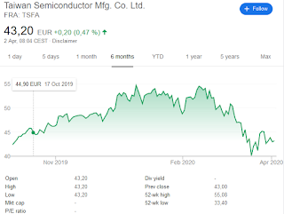
Google Finance (2020-04-02, 10:39 CET)

Sources:

Taiwan shares edge lower, TSMC hit by 3nm delay fears

Our World of data: https://ourworldindata.org/coronavirus

-----------
By Abhishekkumar Thakur, Jonas Sundqvist

Saturday, January 4, 2020

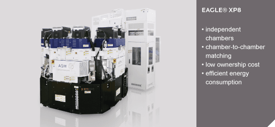
ASM International received TSMC’s Excellent Performance Award for ALD and Epitaxy products

ASM International N.V. (LINK) has received TSMC’s “Excellent Performance Award”, one of seven equipment suppliers to win this recognition in 2019. The award was presented to ASM by Mr. J.K. Wang, Senior Vice President Advanced Fab Operations, at the TSMC Supply Chain Management Forum on Dec 5, 2019, in Taiwan.

The award was received by ASM in recognition of its technology collaboration with TSMC. During the presentation, TSMC explained three points that contributed to the award to ASM. 

1) Outstanding development support.
2) Continuous efforts in productivity improvement.
3) Excellent delivery support on production ramp.

“On behalf of ASM and all of our employees, I thank TSMC for their recognition through this esteemed award,” said Chuck del Prado, CEO and President of ASM International. “Our partnership with TSMC is of strategic importance to ASM. We continuously focus on advancing our leading edge technology, including ALD and Epitaxy products and processes in support of our technology collaborations with TSMC."
 

ASM product portfolio for semiconducttor high volume manufacturing includes ewafer processing equipment for processes such as Atomic Layer Deposition (ALD), Plasma Enhanced ALD (PEALD), Epitaxy, Plasma Enhanced Chemical Vapor Deposition (PECVD), Low Pressure Chemical Vapor Deposition (LPCVD) and Oxidation/Diffusion. (source & credit www.asm.com)

Friday, June 28, 2019

TSMC has presented several research papers at the VLSI Symposium held in Japan.

TSMC has presented several research papers at the VLSI (Very-large Scale Integration) Symposium held in Japan

At the symposium, TSMC covered technologies ranging from pre-package soldering for eMRAM to a new chiplet design based on ARM’s Cortex A72 cores. TSMC also introduced a research paper on tungsten disulphide; a channel material that the fab believes will allow for improved electron flow at 3nm and beyond due to improved 2D electron switching. This tungsten disulphide short-channel transistor is manufactured through chemical vapor deposition directly on the silicon substrate, as opposed to earlier processes that required a sapphire intermediary. One research paper was titled ‘A 7nm 4GHz Arm®-core A72 based CoWoS® Chiplet Design for High-Performance Computing’.
Source: wccftech LINK
----------
By Abhishekkumar Thakur

Thursday, January 3, 2019

Innovation and IP filing in Atomic Layer Deposition has moved from Memory to Logic

By studying the filing of IP world wide one can clearly see the trend how innovation in Atomic Layer Deposition (ALD) has moved from Memory to Logic. During the introduction of ALD (2003 to 2006) in high volume manufacturing of DRAM on 300 mm wafers most IP was filed by Samsung, Micron and SK Hynix. 10 years later (2013-2018) the IP filing lead has been taken over by Logic MPU manufacturers TSMC, Intel and Globalfoundries.

The patent application assignee from the past 25 years.

ASM International received a supplier excellence award from TSMC

[ASM International, LINK] ASM International N.V. (Euronext Amsterdam: ASM) has received a supplier excellence award as one of five equipment suppliers from TSMC for the performance and support of ASM's CVD equipment and technology during 2018. The award was presented to ASM by Dr. C.C. Wei, TSMC's Chief Executive Officer, at the TSMC Supply Chain Management Forum on December 6, 2018 in Taiwan.

The award was received by ASM in recognition of its CVD technology and performance in production at TSMC fabs. During the presentation, TSMC explained three points that contributed to the award to ASM.

1) Close engagement with TSMC and precursor suppliers to innovate process solutions.

2) Continued effort on cost and productivity improvement.

3) Exceptional manpower arrangement for delivery.


"We are very honored to receive this prestigious award from TSMC. On behalf of ASM, I would like to thank TSMC for this recognition," said Chuck del Prado, CEO and President of ASM International. "ASM strives to continuously advance our technology solutions and our partnership with TSMC is of strategic importance to ASM. We are very pleased that TSMC has benefited from the performance of our ALD and Epitaxy deposition tools in its production fabs."

TSMC is the world's largest semiconductor manufacturing foundry. TSMC holds the Supply Chain Management Forum annually to show appreciation for the support and contributions of their suppliers and to recognize outstanding equipment and materials suppliers.

Friday, December 21, 2018

Chinese AMEC 5nm plasma etching tools verified by TSMC

DigiTimes report (LINK) that the Chinese OEM Advanced Micro-Fabrication Equipment (AMEC) announced recently its in-house developed 5nm plasma etching tools have been verified by Taiwan Semiconductor Manufacturing Company (TSMC). AMEC is already among TSMC's equipment suppliers for the foundry's 28nm, 10nm and 7nm processes.

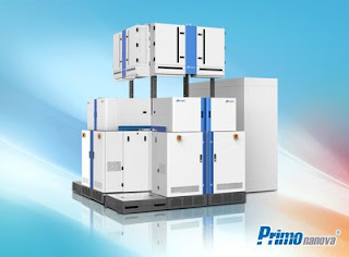
Earlier in 2018 AMEC Introduced the Primo Nanova® System, which is the Company's first ICP etch Product for Chipmakers' most advanced memory and logic (LINK). Besides ICP AMEC has products based on CCP etch and platforms for TSV Etch (LINK).
 AMEC Introduced the Primo Nanova® System (AMEC)

Advanced Micro-Fabrication Equipment Inc. (AMEC)
AMEC is China's leading provider of advanced process technology to global manufacturers of semiconductors and solid-state lighting (SSL) products. Headquartered in Shanghai, the company is an entrenched supplier of dielectric and TSV Etch tools, helping chipmakers build devices at process nodes as low as 7nm. To date, nearly 800 AMEC process units have been positioned at 40 leading-edge semiconductor fabs across Asia. The company is also well established in Europe with AMEC MEMS tools running in production at major IDMs. In addition, with its MOCVD system, the company helps SSL manufacturers build today's most advanced LED products. To learn more about AMEC, please visit www.amec-inc.com.