Showing posts with label ALD2016. Show all posts

Saturday, July 30, 2016

Winners of the ALD2016 Twitter competition - The #ALDToughGirls

Prof. Henrik Pedersen from Linköping university in Sweden won the Twitter competition at ALD2016. He tweeded actively and managed to cover all aspects of the conference - Scientiffically and Socially and personal funny observations. He also made the innoficial #ALDToughGuys vs. #ALDToughGirls competition go to the girls this time. Maybe ALD2017 will have mixed teams #ALDToughScientists instead?


Photos from ALD.com and Twitter.com

Honor should also go to Miia Mäntymäki for being the first Tough Girl on twitter. Later she enjoyed GTs with the toughest of all ALD Scientists, Tero Pilvi from Picosun at the Airport. He can chew gum and talk Swedish at the same time - it is a self-limmited process.

Photo from Tero Pilvi at facebook.com, the moment just before starting to talk Swedish...

Pico Party (twitter.com)

Some asorted looser ALD Tough Guys below:


Pictures from Twitter.com #ALDToughGuys

Wayne State presented new ALD chemistries for low temperature tantalum and selective cobalt at ALD2016

Prof. Chuck Winter and his team at Wayne State presented new ALD chemistries for low temperature tantalum and selective cobalt at ALD 2016 Ireland this week. Both processes are very important for todays scaling of logic and memory technologies. Metallic tantalum can be used in workfunction engineering of HKMG high performance FinFET transitors as well as for Cu seed/barrier technology in BEOL. Cobalt is as tantantlum an option for Cu barrier/seed and also used selectivly to cap the Cu lines and vias from oxidising and reducing RC performance.


The best highlight talk went to Marissa Kerrigan from Wayne State as voted by attendees on novel Co recursor chemistry for selective Cobalt (Left Marissa Kerrigan, right Simon Elliott, photo by ALD2016.com).

“This opens up the prospect of using tantalum in layers just a few nanometers thick as the liner for interconnect wiring in the complex geometries of next-generation electronic chips,” said the University, which worked with German chemicals giant BASF on the project accoring to Electronic Weekly.

Marissa Kerrigan also from Wayne State announced novel ALD chemistry for metallic cobalt that showed excellent selectivity to copper (photo by ALD2016.com).

“The Wayne State processes for tantalum and cobalt are significant steps forward in controlled growth of ultra-thin metals,” said conference chair, Dr Simon Elliott of Ireland’s Tyndall National Institute. “Strong growth is projected for area-selective deposition: in the near future, it will allow higher-precision patterning of semiconductor chips, and in the longer term it will be an enabler for manufacturing nano-structured materials on demand.” according to the same article in Electronics Weekly.

ALD History Blog: ALD history at ALD 2016 Ireland

ALD History Blog: ALD history at ALD 2016 Ireland: Prof Greg Parsons introducing Prof Anatoly Malygin to give a plenary talk at ALD 2016. Photo by Riikka Puurunen. The  ALD 2016  confer...

Friday, July 29, 2016

A breakthrough in Spatial ALD by Dutch research team at HOLST Centre presented at ALD2016 Ireland

A breakthrough materials processing technique devised by a Dutch research team could lead the way for a new generation of smart fabrics, wearable electronics, solar cells and flat-panel displays.

Many of these technologies work by sandwiching together layers of different materials, with some layers ten thousand times thinner than a sheet of paper (just a few nanometres). Such thin layers can be laid down by a technique called atomic layer deposition (ALD), which is the subject of the new research by Holst Centre/TNO in the Netherlands. Improving how the thin layers are deposited is opening up many new opportunities and applications for flexible electronics in everyday life.

ALD is a highly precise technique for the growth of thin material layers. It is primarily used in the fabrication of electronic chips for an array of consumer products such as PCs, tablets and smartphones. Ultra-thin ALD layers in these devices deliver improved speed, energy efficiency, resolution and memory capacity.

The ALD processes used in the semiconductor industry are precise but slow, depositing roughly one nanometre per minute, and must be carried out in specialised vacuum equipment at low pressure on rigid materials. This is acceptable for making chips in the semiconductor industry, but is an obstacle towards using ALD for coating fabrics, foils or TV displays in a standard factory environment. 

 The research team at Holst Centre/TNO, led by Dr Paul Poodt, has successfully brought ALD out of the vacuum to atmospheric pressure, and shortened deposition times to nanometres per second, without compromising on quality. They achieved this by switching to ‘Spatial ALD’ on large-area and roll-to-roll factory equipment that is suitable for coating flexible films and large sheets. (Picture from LinkedIn.com)

The new technique is one of a number of thin film innovations being presented at the 16th International Conference on Atomic Layer Deposition (ALD 2016), which takes place in the Convention Centre Dublin, Ireland on July 24-27.

The team at Holst Centre/TNO started research into Spatial ALD in 2009 and have successfully shown its use in many applications, including a higher efficiency solar cell that is now on the market. Their current goal of coating porous materials and polymers is even more challenging, but could be hugely rewarding.

Paul Poodt, Program Manager at the Open Innovation Institute Holst Centre said: “We needed to understand the role played by gas pressure in Spatial ALD. Porous materials are like microscopic sponges, and molecules need to travel through all the pores, nooks and crannies before coating the pores properly. We found simple equations that tell us that atmospheric pressure does not in fact slow down ALD in porous materials, but can actually help to speed it up. With this understanding we can make clever designs of new Spatial ALD reactors.”

Dr Poodt added: “We believe that Spatial ALD will make flexible electronics possible soon – useful technologies like foldable displays, wearable phones and smart fabrics. We hope that the results we present at the ALD2016 Conference will be the first step to a new range of applications where Spatial ALD can be a key enabling technology.”

Dr Simon Elliott from Tyndall National Institute, chair of the ALD2016 Conference, said: “This exciting result from TNO is a great example of how seemingly-abstract theoretical understanding of gas flow past obstacles can directly impact on the manufacture of new high-tech devices, such as (O)LED lighting, flexible displays and miniature batteries for wearables.”
Dr Paul Poodt and his team will be presenting their research findings on accelerated growth of thin films onto flexible materials as part of the ALD2016 Conference in Dublin. For further information about the ALD2016 Conference please see http://ald2016.com/


Thursday, July 28, 2016

ALD2016 Ireland Photo show

The 16th International Conference on Atomic Layer Deposition (ALD 2016) was a three-day meeting dedicated to the science and technology of atomic layer controlled deposition of thin films. In every year since 2001, the conference has been held alternately in United States, Europe and Asia, allowing fruitful exchange of ideas, know-how and practices between scientists. This year, the ALD conference incorporated the Atomic Layer Etching 2016 Workshop. The conference took place on 24-27 July 2016 at the Convention Centre Dublin, Ireland.

ALD2016 was a grand event and a success! Here I am collecting pictures from the event from Twitter (#ALD2016), The ALD Confernce and others - please send me pictures and I will publish them if you like to share them (jonas.sundqvist@baldengineering.com).


ALD2016 Co-Chairs Simon Elliott (Tyndall National Institute, Ireland) and Jonas Sundqvist (Lund University, Sweden / Fraunhofer IKTS, Germany) taking a final look into the Program before opening the conference on Monday morning. (Picture by ald2016.com)


Opening of ALD2016 by Kieran Drain CEO Tyndall National Institute. (Picture by ald2016.com)


Suvi Haukka from ASM International receiving The ALD Innovation Prize 2016. The prize was presented by last year's awardee Prof. Greg Parsons. (Picture by ald2016.com)


The conference chairs of ALD2016 (Simon Elliott and Jonas Sundqvist) and ALE2016 (Prof. Bert Ellingboe) together with Dennis Hausmann (International & Local Program Committee, Lam Research) learning how to pour a Pint of Gunniess at the Welcome reception that was held at the Guinness Store House in Dublin. (Picture by ald2016.com)

Friday, July 22, 2016

How to get the ALD2016 Ireland Conference App

Before you get on the flight to Ireland you should tak a moment to download teh excellent Conference App that will give you access to the complete program and all abstracts. It is a convienient guide to the conference program and you can write your own notes.


Here is a direct link for :


Beneq strengthens its lead in high-volume industrial ALD

20 July 2016, Beneq, a leading supplier of ALD equipment and thin film coating services, today announced two new thin film equipment solutions for industrial customers that require high capacity and low process cost in advanced ALD applications. The new products are set to revolutionize the standards of coating speed in the ALD industry.

Beneq R11™ – Ultra-fast high precision spatial ALD coating

Beneq R11 is the latest addition to Beneq’s extensive portfolio of large-throughput spatial ALD solutions for industrial use. It provides an optimal solution for high performance ALD on wafers in industrial applications, such as optical coatings, insulators and barriers. It is the ideal choice of equipment when speed, cost, low process temperature and the highest possible film quality are the driving factors.

With Beneq R11, it is for the first time possible to use PEALD (Plasma Enhanced ALD) processes in high volume manufacturing. The system lends itself to barrier, insulation and anti-corrosion applications for MEMS, LED, OLED, photovoltaics, high power semiconductors, sensors and many other components.

The equipment is suitable for up to 200 mm wafers and other round or rectangular substrates. The plasma enhanced rotary ALD process of Beneq R11 is ideal for thick ALD films, in the micrometer thickness range. Beneq R11 can also be equipped with standard wafer automation.


Beneq T2S™ – Automated batch wafer equipment

Beneq T2S is the newest member of Beneq’s wafer-based production equipment portfolio. It offers a unique combination of high capacity batch processing and standard cassette-to-cassette automation. The Beneq T2S is specifically engineered to match the semiconductor requirements, including the SEMI S2 safety requirements and low particle counts.

Beneq T2S is perfectly suited for high volume manufacturing in various wafer-based applications, including MEMS, LED, OLED, ink-jet print heads and more. The thermal batch ALD process of Beneq T2S is ideal for oxide and nitride processes used for dielectric, conductor, barrier and passivation purposes.

The equipment is designed for wafers up to 200mm in diameter and can process 25 wafers per run in face-down or face-up orientation.

New products officially unveiled in ALD2016 in Dublin, Ireland

Both new products, Beneq R11 and Beneq T2S, will be introduced officially for the first time next week at ALD2016 – the 16th International Conference on Atomic Layer Deposition, which will be held at the Convention Centre Dublin, Ireland, 24-27, July 2016. Beneq is a platinum sponsor of the event.

Says Tommi Vainio, Vice President, Thin Film Equipment, at Beneq: “High capacity industrial ALD solutions are an important and expanding part of our product portfolio. Our commitment to revolutionize the coating speed standards in the ALD industry is clearly demonstrated in the new ALD equipment we are launching in Dublin. From now on with Beneq, the unit for ALD area is m2 instead of mm2.”

More information about the new products and the multitude of Beneq ALD applications is available at the Beneq stand in the ALD exhibition of the conference. The number of the Beneq booth is 30. You can also visit Beneq Monday through Wednesday at the Beneq Boat Bar right next to the convention centre.

Thursday, July 21, 2016

Ultratech CNT in Dublin at ALD2016 presenting latest work on Superconductivity, SAMS Area-Selective ALD (ASD), Molybdenum Nitride and product developments

The Platinum Sponsor, supporting over 450 ALD research systems worldwide, will bring its science team to the ALD conference to present latest work and discuss leading edge application developments with delegates. Available at booth #15 and presenting as follows.


Plasma enhanced atomic layer deposition of molybdenum nitride
Adam Bertuch*1, Brent Keller2, Ganesh Sundaram1, Jeffrey Grossman2
1Ultratech - Cambridge NanoTech, USA, 2Department of Material Science and Engineering, Massachusetts Institute of Technology, USA
Tuesday 26 July:  Plasma-enhanced deposition and etching  -  Tuesday 26 July 15:45-17:15
16:30-16:45
Controlling smoothness of thin platinum ALD films
Ritwik Bhatia*1, Ralf Heilmann2, Alexander Bruccoleri3, Brandon Chalifoux2
1Ultratech-Cambridge Nanotech, USA, 2Massachusetts Institute of Technology, USA, 3Izentis LLC, USA
Wednesday 27 JULY:  Noble metals  -  Wednesday 27 July 08:15-10:15
10:00-10:15
Plasma enhanced atomic layer deposition of superconducting NbN films
Mark Sowa*1, Yonas Yemane2, J Provine3, Fritz Prinz4
1Ultratech/CNT, USA, 2Stanford University, Department of Applied Physics, USA, 3Stanford University, Department of Electrical Engineering, USA, 4Stanford University, Department of Mechanical Engineering and Department of Materials Science and Engineering, USA
Tuesday 26 July:  Poster session 2  -  Tuesday 26 July 17:15-19:00


Sunday, July 17, 2016

2016 General meeting of HERALD at ALD Conference

The 2016 general meeting of the HERALD COST Action MP1402 will take place during the 16th International Conference on Atomic Layer Deposition, which is taking place in the Convention Centre Dublin, Ireland, on 24th-27th July 2016. The final morning of the conference is being devoted to HERALD, in parallel with other conference sessions.

27th July 2016, Liffey Hall 1:

8:45-10:15 HERALD Showcase: Presentation by working group leaders of scientific collaborations in each WG, with opportunity for discussion from all members. Discussion of HERALD targets for widening participation and structuring the ALD community in Europe in the future.

10:15-11:00 HERALD Poster Session: Opportunity for all members to display and discuss posters. There will be no review or selection of abstracts, but the intention to display a poster must be indicated via registering on the eventbrite page by 13th July.

11:00-12:30 Launch of HERALD White Paper on 'Atomic-level processing' and panel discussion: A panel discussion on the future of atomic-level processing for European manufacturing, and in the global context. All are welcome to attend and put their questions to the panellists.

The HERALD sessions are open to all delegates of the ALD2016 conference at no extra fee. HERALD members are strongly encouraged to attend. Travel reimbursements through HERALD are not available, except for the collaboration competition that was previously advertised.


Please register your intention to attend part or all of the HERALD sessions via this eventbrite page by 13th July, so as to facilitate seating, catering and poster boards:

https://www.eventbrite.com/e/herald-sessions-at-ald2016-ireland-tickets-26329089014

The password for the eventbrite page is HERALD 

Tuesday, July 12, 2016

Oxford Instruments to present recent developments in ALD and ALE in Dublin at ALD2016

Oxford Instruments, a company that truly master both Atomic Layer Deposition and Atomic Layer Etching, will be giving two talks at the Joint 
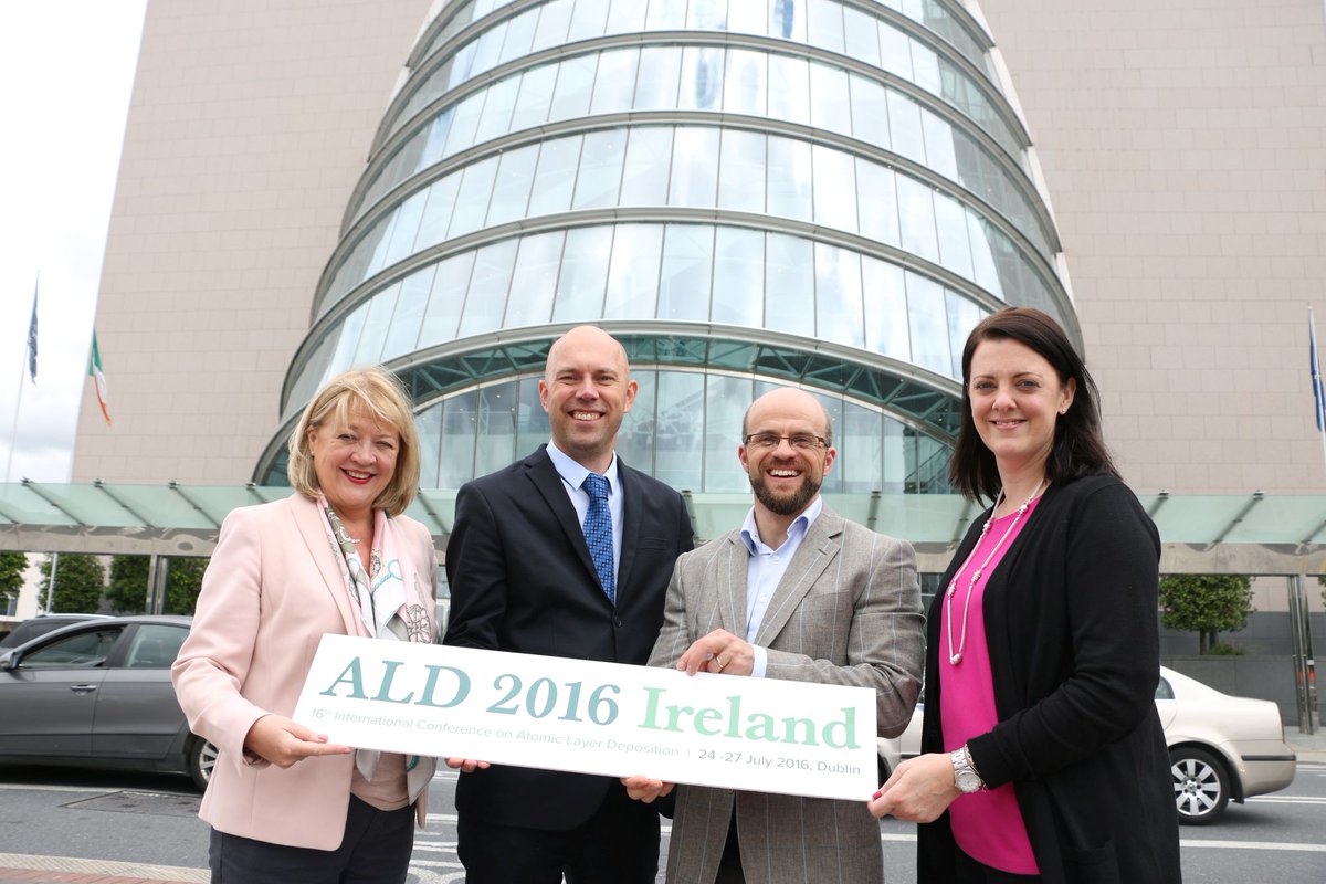
ALD2016 Conference and ALE2016 Workshop in Dublin, Ireland in less than two weeks. Naturally one on each topic!

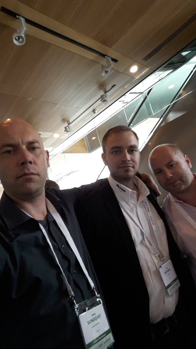
Oxford Instruments is Platinum sponsor of the conference and you will have an opportunity to meet with their Deposition and Etch Experts at the Exhibition and Social events.

Harm Knoops
Oxford Instruments Plasma Technology, UK / Researcher at TU Eindhoven, NL
Low-temperature plasma ALD of silicon nitride moisture barrier layers

Wednesday 27 JULY: Silicon-based materials - Wednesday 27 July 14:00-15:30
15:15-15:30

ALD has demonstrated to be able to provide excellent moisture barrier layers, which are vital for the encapsulation of organic (opto-)electronic devices, such as organic light-emitting diodes (OLEDs) and thin-film photovoltaic cells. Very low water vapor transmission rates (WVTR) have been shown using oxide layers prepared by ALD (Al2O3 and TiO2) but not yet for nitride layers. In this work, moisture permeation barrier layers of SiNx prepared by ALD using SiH2(NHtBu)2 (BTBAS) precursor and Ar-N2 plasma were investigated.1 Intrinsic WVTR values in the range of 10−6 g/m2/day were obtained, indicating excellent barrier properties for ALD SiNx layers as thin as 10 nm.


Mike Cooke, CTO
Oxford Instruments, UK
Atomic layer etching (ALE) in close-to-conventional plasma etch tools

Tuesday 26 July: Plasma-enhanced deposition and etching - Tuesday 26 July 15:45-17:15
15:45-16:15

Plasma etching equipment and expertise is widespread, and cyclical etch processes are well known for high rate silicon etching. With the recent surge in interest in atomic layer etching, many groups are attempting to perform ALE in their existing tools. This talk discusses the limitations and options of using conventional tools for ALE, and gives results for both conventional and modified equipment.


Oxford Instruments releasing new innovative hardware for ALE (Atomic Layer Etching) Harm Knoops at SEMICON Europa 2015, Dresden, Germany.
In addition, you may be interested in talk given by Dmitry Suyatin on III/V Nanowire splitting by ALE - work all performed on an Oxford Instruments Plasmalab 100 at Lund Nano Lab, Sweden

Dmitry Suyatin
Staff Engineer, Lund Nano Lab, Lund University, Sweden
Monday 25 July, Monday 25 July 13:45-15:15
Liffey Hall 1
Workshop: Non-traditional ALE approaches

To study the ALE process for III/V nanowires GaP nanowires were grown by metal organic vapor phase epitaxy (MOVPE) from gold seed particles on GaP substrates and then mechanically transferred to Si surface. An ALE process optimized for Si etching was used to etch the GaP nanowires by applying a 30 nm (105 cycles) etch recipe. Surprisingly, we discovered that we were able to split the nanowires longitudinal into too wires (as shown in Figure 1, below).


Meet Picosun at ALD2016 Ireland and join the PicoParty(TM)

Picosun is announcment: Meet #Picosun at Stand #40 at #ALD2016_Ireland! Claim your gift, win an iPad - and don't forget the PicoParty™!

Monday, July 11, 2016

ALD 2016 panel discussion atomic-level processing

At this years ALD Confernce in Ireland there will be a panel discusion a panel discussion on the future of atomic-level processing for European manufacturing, and in the global context. The discussion is co-hosted by the HERALD COST Action, but all are welcome to attend and put their questions to the panellists. 

As important background information you are all very much welcome to download the white paper "The future of atomic level processing" written by Simon Elliott, Co-Chair of ALD2016 and initiator and Chair of the HERALD COST Action.
Executive Summary
Atomic-level control of materials processing will be needed in the semiconductor industry within the next 5-10 years, and will be a powerful enabling technology for other high-tech manufacturing sectors. This will be possible if atomic-level precision can be achieved with the traditional fabrication steps – deposition, patterning and etching. There is therefore a strong need for coordinated research now into how the current concept of atomic layer deposition may be developed into selective-area patterning and atomically controlled etching.


White Paper download: LINK

The panel will be moderated by Jonas Sundqvist, co-chair of ALD2016 and the current panel members are:
  • Dr. Suvi Haukka, ASM Microchemistry, Finland
  • Dr. David Thompson, Applied Materials, USA
  • Dr. Jean-Marc Girard, Air Liquide, France
  • Prof. Mikko Ritala, University of Helsinki, Finland
  • Prof. Fred Roozeboom, Eindhoven University of Technology / TNO - Solliance, The Netherlands"

PLEASE SUBMIT YOUR QUESTIONS TO

Chair: Jonas Sundqvist (jonas.sundqvist@baldengineering.com)
Link: LINK


Dublin, Ahoy! Beneq will be everywhere at ALD2016

As promoted by Beneq - The ALD event of the year is approaching. As you know, Beneq is a platinum sponsor of ALD 2016 (the 16th International Conference on Atomic Layer Deposition), which will be held at the Convention Centre Dublin, Ireland, 24-27, July 2016. 
If you are coming to the event (it is not too late too book!), you can find us everywhere at the event: we will have a stand at the exhibition, we have several presentations in the conference, and we will have a large event team you can book meetings with.

Meet us at the Beneq ALD Boat Bar

This year, there is also a new attraction: The Beneq ALD Boat Bar. It will be our meeting room, lounge area and the heart of the best ALD discussions. The bar will be open every day of the event (Monday through Wednesday) in the White Bar of MV Cill Airne, right next to the convention centre.

You are cordially invited to join us for a pint on board. We believe that the discussions at our boat bar will be what this year’s ALD conference will be remembered for. Get in touch with your favorite Beneq person to get your personal invitation!

Meet us at Booth number 30

The conference also comprises an ALD exhibition. On the Beneq stand, we will have many interesting ALD objects on show, from the latest research samples to a selection of ALD coated end products.

This is also where you can get more information about the multitude of ALD applications we have been working with and all our latest products (stay tuned for more exciting product news before the event!). The number of the Beneq booth is 30. Come and take a look.

Meet us in Beneq presentations at ALD2016

The Beneq team also has several presentations in conference program. Here are the details:

1) Sami Sneck will be speaking in the session Transparent conductive oxides and optical applications 1 in the morning of Wednesday July 27th. His presentation is about Development of the world's most transparent display - enabled by ALD.

2) Mikko Söderlund will be presenting about Large area sheet-to-sheet spatial ALD system for high-throughput coating applications in poster session 2 on Tuesday 26th of July.

3) In the same poster session, also Kari Härkönen from our Development Services team will be presenting. His topic is ALD-based 3D NIR filter and refractive index control for Rugate filters.

We are all set and ready to board. See you in Dublin!

Sunday, July 10, 2016

Updates and information for ALD 2016 Conference – 24 – 27 July in Dublin, Irleand

Here are some recent updates and information for ALD 2016 Conference – 24 – 27 July.


Speakers and Conference Programme

The conference programme for the the conference can be viewed here.

Delegate Information

Delegate information detailed here to help you plan your visit to Dublin: 
http://ald2016.com/delegate-information/

Poster printing:

Details regarding the format for printing can be found here:  Poster Printing Instructions for ALD2016.  Please note that all authors are required to print their own posters and the document includes details of a local company that is located close to the Convention Centre.

ALD2016 Exhibitors

Information regarding set up at The CCD and conference information can be found here: http://ald2016.com/exhibition-information/

Wednesday, June 29, 2016

Atomic Layer Etch Heats Up - ALE 2016 Ireland up next

In less then a month the ALE 2016 Workshop is on together with ALD2016 in Ireland. Here is a fresh article on ALE by Mark Lapedus at Semiconductor Engineering:

The atomic layer etch (ALE) market is starting to heat up as chipmakers push to 10nm and beyond. ALE is a promising next-generation etch technology that has been in R&D for the last several years, but until now there has been little or no need to use it. Unlike conventional etch tools, which remove materials on a continuous basis, ALE promises to selectively and precisely remove targeted materials at the atomic scale.

It now is moving from the lab to the fab. Applied Materials, for example, has officially entered the next-generation etch market by rolling out a new tool technology. Applied describes its technology as an “extreme selectivity” etch tool, although the system basically falls in the generic category of ALE.

Meanwhile, Hitachi High-Technologies, Lam Research and Tokyo Electron Ltd. (TEL) are also working on ALE tools.

Monday, June 20, 2016

Picosun are sponsoring and attending the ALD 2016 Conference in Ireland

Picosun is the leading provider of high quality Atomic Layer Deposition (ALD) thin film coating equipment and solutions for global industries and R&D will be participating at ALD2016 in Ireland as well as providing a Platinum Sponsorship of the event.

The 16th International Conference on Atomic Layer Deposition (ALD 2016) will be a three-day meeting dedicated to the science and technology of atomic layer controlled deposition of thin films.  In every year since 2001, the conference has been held alternately in United States, Europe and Asia, allowing fruitful exchange of ideas, know-how and practices between scientists. This year, the ALD conference will incorporate the Atomic Layer Etching 2016 Workshop, so that delegates at the two events can interact freely.  The conference will take place on 24-27 July 2016 at the Convention Centre Dublin, Ireland.


Come meet Picosun Team at the ALD 2016 Dublin!
For the latest and the brightest from The ALD Powerhouse visit
BOOTH #40

Friday, June 17, 2016

ALD 2016 Final day for reduced conference registartion today!


Conference Registration


16th International Conference on Atomic Layer Deposition (ALD 2016 Ireland) incorporating Atomic Layer Etching 2016 Workshop:

Early Registration: closed on 31 March 2016
Standard: 1 April to 17 June 2016
Late Registration: 18 June to 18 July 2016
button-register

Delegate Student
Early Stnd Late Early Stnd Late
ALD 2016 Full Conference Pack
  • Entry to Tutorial on Sunday 24 July 2016
  • Conference attendance Monday 25 to Wednesday 27 July 2016
  • Access to all oral and poster sessions
  • Attendance at Atomic Layer Etching Workshop on Monday 25 July
  • Lunch and refreshments at CCD
  • Conference material
  • Welcome Reception in the Guinness Storehouse on Sunday 24 July 2016
  • Gala Dinner on Wednesday 27 July 2016
n/a €730 €770 n/a €545 €575
ALD 2016 Conference Delegate Rate  
  • Conference attendance Monday 25 to Wednesday 27 July 2016
  • Access to all oral and poster sessions
  • Attendance at Atomic Layer Etching Workshop on Monday 25 July
  • Lunch and refreshments at CCD
  • Conference material
  • Welcome Reception in the Guinness Storehouse on Sunday 24 July 2016
  • Gala Dinner on Wednesday 27 July 2016
n/a €580 €620 n/a €435 €465
3rd International Atomic Layer Etching 2016 Workshop
  • Attendance at the Welcome Reception at the Guinness Storehouse on Sunday 24 July 2016
  • Attendance at Atomic Layer Etching 2016 Workshop as well as the full conference programme on Monday 25 July 2016
  • Refreshments and conference materials
n/a €260 €300 n/a €195 €225
One Day Delegate (Monday 25 – Wednesday 27 July 2016)
  • One day conference attendance
  • Access to all oral and poster sessions
  • Lunch and refreshments
  • Conference material
  • Welcome Reception in the Guinness Storehouse on Sunday 24th July 2016 (for delegates registered for Monday 25 or Tuesday 26 July)
  • Gala Dinner on Wednesday 27 July 2016 (for delegates registered for 27 July)
n/a €260 €300 n/a €195 €225
Sunday Tutorial – 24 July 2016
  • Attendance at tutorial
  • Conference materials
  • Refreshments
n/a €150 €175 n/a €110 €130
Exhibitor
  • Access to Exhibition only on Monday 25, Tuesday 26 and Wednesday 27 July 2016
  • Refreshments and lunch
€350
(Please note that the exhibitor pass is only applicable to organisations that have booked and have received confirmation of an exhibition stand at the conference)
To register for ALD 2016 please click here to select your attendee type and to complete the online registration form. At the end of the registration process you will be required to make payment by credit card and once complete, you will receive an email confirming your booking at the conference. You will be asked to create a username and password as part of the registration process and this will enable you to make amends to your booking if required in the lead up to the conference.
Early Bird Conference Registration:
The early bird conference rate closed on the 31 March 2016.
Atomic Layer Deposition and Atomic Layer Etching:
You can register for ALD2016 (one day or three days, 25-27 July) and the Atomic Layer Etch workshop (one day, 25 July), as well as for the joint ALD/ALE tutorial (half-day, 24 July). As part of the registration process and for tracking purposes, we ask that you indicate your primary interest in Atomic Layer Deposition or Atomic Layer Etching.
Student identification:
Please note that students will be required to show their current student identification card at registration onsite at the conference. If no card is shown, the outstanding balance for the full conference fee will be taken before admission to the conference.
Abstract submission:
Please note that abstract submission is a separate online form. Author/s who have submitted abstracts must register their place/s too.
Visa application / invitation letters:
Information regarding visa application / invitation letters can be found on venue, accommodation, travel and visas page of this website.

Registration Cancellations:

Cancellations received 30 days prior to the conference will be charged an administration charge of 20% of the Conference fee plus the service charge.
Cancellations made 29 days prior to the start of the conference or later, as well as ‘no shows’, are liable for the full registration fee. Name changes to existing bookings are permitted up until close of registration on Friday 15th July 2016.

Thursday, June 2, 2016

Speaker & Abstracts for Atomic Layer Etching 2016 Workshop in Dublin

Now the complete program for the ALE 2016 Workshop that runs in parallel to ALD2016 in Dublin has been released. Plead find the programme and links to abstract below.


Monday 25 July, Monday 25 July

Thermal ALE

10:45-12:15
Liffey Hall 1
Workshop: Thermal ALE
Chair: to be confirmed
O17 Developments in Thermal Atomic Layer Etching Using Sequential, Self-limiting Reactions
Steven George*, Younghee Lee, Jaime DuMont, Nicholas Johnson, Amy Marquardt
University of Colorado, USA
10:45-11:15
O18 Isotropic atomic layer etching of silicon nitride for 3D device applications
Kazunori Shinoda*1, Nobuya Miyoshi1, Hiroyuki Kobayashi1, Masaru Kurihara1, Tadamitsu Kanekiyo2, Masaru Izawa2, Kenji Ishikawa3, Masaru Hori3
1Hitachi, Japan, 2Hitachi High-Technologies, Japan, 3Nagoya University, Japan
11:15-11:45
O19 Low-Temperature Selective Tungsten Hexafluoride Chemical Vapor Etching of TiO2 Films
Paul Lemaire*, Gregory Parsons
North Carolina State University, USA
11:45-12:00
O20 A two-step atomic layer etching process on MoS2 realized by remote O2 plasma
Hui Zhu, Xiaoye Qin, Lanxia Cheng, ANgelica Azcatl, Jiyoung Kim, Robert Wallace*
University of Texas at Dallas, USA
12:00-12:15


Non-traditional ALE approaches

13:45-15:15
Liffey Hall 1
Workshop: Non-traditional ALE approaches
Chair: to be confirmed
O32 Longitudinal nanowire splitting by atomic layer etching
DMITRY B. SUYATIN*, MD SABBIR AHMED KHAN, JONAS SUNDQVIST, ANDERS KVENNEFORS, MARIUSZ GRACZYK, NICKLAS NILSSON, IVAN MAXIMOV
Lund University, Sweden
13:45-14:00
O33 A novel atomic layer etching of SiO2 with alternating O2 plasma with fluorocarbon film deposition
Takayoshi Tsutsumi*1, Masaru Zaitsu2, Akiko Kobayashi2, Hiroki Kondo1, Toshihisa Nozawa2, Nobuyoshi Kobayashi2, Masaru Hori1
1Nagoya University, Japan, 2ASM Japan K. K., Japan
14:00-14:15
O34 Towards wet-chemical atomic layer etching of III-V and Ge for N7 and N5 technology nodes
Dennis H. van Dorp*, Sophia Arnauts, David Weinberger, Farid Sebaai, Niamh Waldron, Frank Holsteyns
Imec, Belgium
14:15-14:45
O35 Accelerated Neutral Atom Beam Procssing for Atomic Level Etch
Craig Huffman*1, Francis Goodwin1, Satyavolu Papa Rao1, Brendan O'Brien1, Edward Barth1,4, Saikumar Vivekanand3, Martin Rodgers3, Sean Kirkpatrick2, Michael Walsh2,4, Richard Svrluga2,4
1SUNYPoly SEMATECH, USA, 2Exogenisis Corporation, USA, 3CNSE SUNYPoly, USA, 4Neutral Physics Corporation, USA
14:45-15:00
O36 InGaAs Atomic Layer Etching
Jinwoo Park*, Geunyoung Yeom
Sungkyunkwan University, Republic of Korea
15:00-15:15


Advances in applications and hardware of ALE

15:45-17:15
Liffey Hall 1
Workshop: Advances in applications and hardware of ALE
Chair: to be confirmed
O48 Plasma source configuration impact on surface processes for high precision etch
Akira Koshiishi*1, Alok Ranjan2, Peter Ventzek3
1Tokyo Electron Miyagi Ltd., Japan, 2TEL Technology Center, America, LLC, USA, 3Tokyo Electron America, Inc., USA
15:45-16:15
O49 Electron Beam Generated Plasmas: An ultra low Te route toward ALEt
David Boris*, George Petrov, Tzvetelina Petrova, Scott Walton
U.S. Naval Research Laboratory, USA
16:15-16:30
O50 Investigating the role of neutral transport in ALE and RIE processes using a 3-dimensional Monte Carlo Feature Profile Model
Chad M. Huard*1, Mark J. Kushner1, Yiting Zhang2, Saravanapriyan Sriraman2, Alex Paterson2
1University of Michigan, USA, 2Lam Research Corp., USA
16:30-16:45
O51 Atomic layer processing by conventional and low electron temperature plasma sources: a feasibility study
Hiroyuki Miyazoe*1, Ashish Jagtiani1, Josephine Chang1, Demon Farmer1, Michael Engel1, Deborah Neumayer1, Shu-Jen Han1, Sebastian Engelmann1, David Boris2, Sandora Hernández2, Evgeniya Lock2, Scott Walton2, Eric Joseph0
1IBM TJ Watson Research Center, USA, 2Naval Research Laboratory, USA
16:45-17:00
O52 Atomic Layer Etching of Silicon Nitride using Hydrofluorocarbon Chemistry
Yohei Ishii*, Kazumasa Okuma, Tiffany Saldana, Nobuyuki Negishi, Jim Manos
Hitachi High Technologies America, Inc., USA
17:00-17:15


ALD Lab Saxony at ALD2016

ALD Lab Saxony presenting oral presentations at ALD2016


Wege, Stephan
plasway-Technologies GmbH, Germany
Plasma Processing Reactor Design
Sunday 24 July: Tutorial: Plasma processing - Sunday 24 July 14:15-15:45
14:45-15:15

Hossbach, Christoph
TU Dresden, Institute of Semiconductors and Microsystems, Germany
Organic electronic devices with inorganic high-k gate oxides grown by Atomic Layer Deposition
Tuesday 26 July: High-k dielectrics 1 - Tuesday 26 July 08:45-10:15
09:15-09:30

Junige, Marcel
Technische Universität Dresden, Germany
The ALD of Ru and RuO2 – An intertwined special case
Wednesday 27 JULY: Noble metals - Wednesday 27 July 08:15-10:15
09:15-09:30

Knaut, Martin
Technische Universtität Dresden, Institute of Semiconductors and Microsystems, Germany
Atomic layer deposition and 3D nanoscale substrates - nanowires, nanotubes and nanopores
Wednesday 27 JULY: High aspect ratio nanostructures - Wednesday 27 July 16:00-17:30
16:00-16:15

Wednesday, June 1, 2016

ALD2016 Speakers and Conference Programme announced!

The conference programme for the The 16th International Conference on Atomic Layer Deposition, Dublin Ireland can now be viewed here.

Conference Timings:

Sunday 24 July:

Tutorial runs 13:00-17:00 in Convention Centre. Welcome reception that evening in Guinness Storehouse.

Monday 25 July – Wednesday 27 July:


ALD2016 Conference will open at 8:15 in Convention Centre and closes at 17:45 on Wednesday 27 July followed by a gala dinner on Wednesday evening.

Opening plenary invited talk by Prof. Lars Samuelson, NanoLund, Lund University Sweden followed by Prof. Anatolii Malygin, Saint-Petersburg State Institute of Technology, Russia and Ankur Agarwal, Applied Materials, USA.

ALD 2016 Conference Logo
The 16th International Conference on Atomic Layer Deposition (ALD 2016) will be a three-day meeting dedicated to the science and technology of atomic layer controlled deposition of thin films. In every year since 2001, the conference has been held alternately in United States, Europe and Asia, allowing fruitful exchange of ideas, know-how and practices between scientists. This year, the ALD conference will incorporate the Atomic Layer Etching 2016 Workshop, so that delegates at the two events can interact freely. The conference will take place on 24-27 July 2016 at the Convention Centre Dublin, Ireland.

Atomic Layer Deposition (ALD) is used to fabricate ultrathin and conformal thin film structures for many semiconductor and thin film device applications. A unique attribute of ALD is that it uses sequential self-limiting surface chemistry to achieve control of film growth in the monolayer or sub-monolayer thickness regime. ALD is receiving attention for its applications in leading-edge electronic technologies, advanced microsystems, displays, energy capture and storage, solid state lighting, biotechnologies and medical technologies. Indeed ALD is particularly advantageous for any advanced technology that requires control of film structure in the nanometer or sub-nanometer scale.

As in past conferences, the meeting will be preceded by one day of tutorials. An industry trade show will be held in conjunction with the conference, to act as common ground for academia and industry to meet and discuss the future applications of ALD. Extra opportunities for collaboration will be provided through working groups of the COST Action ‘Hooking together European research in atomic layer deposition (HERALD)’.

This conference offers an excellent opportunity to learn about the most recent R&D activities in ALD science and technology from researchers around the world. We look forward to your participation.

ALD 2016 Co-Chairs:
Simon Elliott, Tyndall National Institute , Ireland Jonas Sundqvist, Division of Solid State Physics, Lund University, Sweden
Simon Elliott
Tyndall National Institute,
Ireland
Jonas Sundqvist
Division of Solid State Physics,
Lund University, Sweden