Thursday, June 8, 2023

Global semiconductor equipment billings rise 9% YoY to $26.8B in Q1 2023. Taiwan up 42%, China down 8%, North America soars 51%. Strong AI and automotive investments.

US Fab expansion kick in - The global semiconductor equipment billings rose 9% YoY to $26.8B in Q1 2023, despite challenging conditions. Taiwan saw 42% growth, while China dropped 8%. North America surged by 51%. Long-term investments for AI and automotive remain strong.


As an excerpt from a news release by SEMI - here are some key points from the report:

Global Semiconductor Equipment Billings - In the first quarter of 2023, global semiconductor equipment billings reached US$26.8 billion, representing a 9% increase compared to the same period in the previous year. However, billings slipped 3% when compared to the previous quarter.

Regional Billings

The data provided breaks down the billings by region and shows the quarter-over-quarter and year-over-year changes. Here are some notable regional highlights:Taiwan: Billings of $6.93 billion, with a 13% decrease compared to the previous quarter but a significant 42% increase year-over-year.

  • China: Billings of $5.86 billion, reflecting an 8% decrease quarter-over-quarter and a 23% decrease year-over-year.
  • Korea: Billings of $5.62 billion, showing a slight 3% decrease quarter-over-quarter but a positive 9% increase year-over-year.
  • North America: Billings of $3.93 billion, indicating a substantial 51% increase quarter-over-quarter and a significant 50% increase year-over-year.
  • Japan: Billings of $1.90 billion, with a 16% decrease quarter-over-quarter but no change year-over-year.
  • Europe: Billings of $1.52 billion, reflecting a 4% increase quarter-over-quarter and a 19% increase year-over-year.
  • Rest of World: Billings of $1.06 billion, experiencing a 20% decrease quarter-over-quarter and an 18% decrease year-over-year.
Market Outlook: Despite macroeconomic challenges and a difficult industry environment, semiconductor equipment revenue in the first quarter was robust. The long-term strategic investments needed to support major technology advancements for applications like AI (Artificial Intelligence) and automotive remain healthy.

SEMI Equipment Market Data Subscription (EMDS): SEMI offers a subscription service providing comprehensive market data for the global semiconductor equipment market. It includes monthly reports on equipment market trends, semiconductor equipment billings by region and market segments, and an outlook for the semiconductor equipment market.

https://semi.org/en/news-media-press-releases/semi-press-releases/q1-2023-global-semiconductor-equipment-billings-grow-9%25-year-over-year-semi-reports

Wednesday, June 7, 2023

US company Forge Nano raised US$50 M with Korea's Hanwha Corporate Venture Capital for Battery Pilot Line

US company Forge Nano has successfully raised over $50 million in its recent funding round, with Korea's Hanwha Corporate Venture Capital leading the investment. Other participants included Orion Infrastructure Capital, Catalus Capital, Ascent Funds, and existing investors. This funding brings Forge Nano's total capital raised to date to over $95 million.


The funds will enable Forge Nano to seize the growing opportunities in commercial-scale nanotechnology for battery materials and establish a battery production line capable of meeting the demand for premium batteries. The company plans to commence construction of a pilot battery production line in the second quarter of 2023, catering to various industries such as aerospace, consumer electronics, and defense.

Forge Nano's proprietary technology, known as Atomic Armor, is widely employed in battery applications for vehicles, aerospace, consumer electronics, defense, and other high-end Li-ion users. With this new funding, Forge Nano aims to further develop and scale its Atomic Armor technology within the lithium-ion market, enabling the company to offer finished battery solutions at scale.

The funding will also enhance Forge Nano's capabilities in applying Atomic Armor across different industries. By expanding its manufacturing footprint and allocating more resources to customer support, the company expects to increase its production capacity fivefold while improving tool production efficiency through the integration of digital management infrastructure.

Forge Nano has recently formed strategic partnerships with prominent U.S. material producers and battery off-takers, highlighting the capabilities of its proprietary nanocoating technology, Atomic Armor. These partnerships aim to develop next-generation batteries and strengthen the U.S. domestic battery supply chain. For instance, Forge Nano's collaboration with Anovion, a U.S.-based battery material producer, combines Forge Nano's surface engineering expertise with Anovion's synthetic graphite to create industry-leading lithium-ion batteries.

The company foresees substantial revenue growth in 2023 and expects to double its revenue once again through increasing market adoption. Forge Nano's Atomic Armor technology empowers manufacturers to engineer materials at the atomic level, optimizing battery characteristics such as range, safety, and cycle life. With a team of experienced scientists and a broad portfolio of commercial partners, Forge Nano offers tailored solutions across the entire spectrum, from small-scale research and development to large-scale, high-volume production.

Source:

Tuesday, June 6, 2023

TNO heads consortium developing ‘Third-generation electrolyzers with SparkNano ALD technology

Dutch research center TNO, along with three technical universities and several enterprises, is leading a consortium to develop "Third-generation electrolyzers," aiming to create more affordable and efficient electrolyzers for hydrogen production. 

The collaboration will focus on designing advanced stacks and components for electrolysers, as well as exploring manufacturing technologies. The goal is to establish a significant presence in the global electrolyser market. The five-year project will investigate various methods of water splitting and CO2 electrolysis, with the expectation that different concepts will synergize and contribute to the development of cutting-edge production technology. 


TNO's Atomic Layer Deposition technology, marketed by SparkNano, holds promise for creating novel electrolysers. The initiative is part of NXTGEN HIGHTECH, which aims to provide innovative solutions in key areas of production technology. Participating companies, knowledge institutions, and groups include Admatec, Bosch Transmission Technology, Coval Energy, Delft University of Technology, Eindhoven University of Technology, Magneto Special Anodes, and others.

Links &sources:

TNO heads consortium developing 'Third-generation electrolyzers' - (industryandenergy.eu)

News | P2Hydrogen - VoltaChem

Home - NXTGEN Hightech

SparkNano | Spatial Atomic Layer Deposition (ALD) technology (spark-nano.com)

Friday, June 2, 2023

ASM breaks ground on new state-of-the-art innovation and manufacturing center in Hwaseong, Korea

ASM International N.V. is embarking on the construction of a state-of-the-art innovation and manufacturing center in Hwaseong, South Korea. With a groundbreaking ceremony to be held soon, the expansion project is part of ASM's US$100 million investment plan and follows a Memorandum of Understanding signed with the Ministry of Trade, Industry and Energy of South Korea. The investment aims to bolster ASM's research and product development infrastructure and increase manufacturing capacity to meet the growing demand for semiconductors. The company also intends to create job opportunities in engineering, R&D, and manufacturing, contributing to workforce development in Korea.


The ceremony will be attended by ASM's CEO, Benjamin Loh, and other dignitaries, including political figures and business partners. Loh expressed his enthusiasm for the expansion in Hwaseong, highlighting the potential and dedication of the Korean people. The investment signifies ASM's commitment to Korea and its ambition to grow the business while enabling the development of advanced technologies in the semiconductor industry. Hwaseong has played a vital role in ASM's growth, serving as a hub for advanced R&D and technology for both local and global customers.

The existing Hwaseong facility, which currently employs over 450 people, will be expanded to accommodate more employees as the company continues to grow. The new extension will add 31,000 m2 across eight floors, more than doubling the facility's R&D area and nearly tripling its manufacturing area. YK Kim, Chairman of ASM Korea, emphasized that the expansion is an investment in people and the semiconductor ecosystem in Korea, aiming to support the country's semiconductor industry growth in collaboration with the government, customers, and suppliers.

ASM's commitment to Hwaseong demonstrates its dedication to the Korean market and its goal of facilitating domestic semiconductor innovation while meeting global customer demands. The company's local R&D team has been instrumental in developing groundbreaking technologies in the industry, such as ALD QCM quad chamber modules, TENZA™ ALD for high aspect ratio gap-fill, and high-quality PEALD silicon and metal oxides and nitrides for various applications. 

Release of TENZA(TM): BALD Engineering - Born in Finland, Born to ALD: ASM International launches TENZA ALD Quad Chambers for silicon oxide gap-fill and liners on the XP8 platform


ASM Korea MOU: BALD Engineering - Born in Finland, Born to ALD: Dutch ALD euipment leader ASM to invest $100 mil. in Korea for facility expansion


Finnish ALD equipment manufacturer Beneq has entered a partnership with Lung Pien Vacuum Industry Co., Ltd. in Taiwan.

Finnish ALD equipment manufacturer Beneq has partnered with Taiwan's Lung Pien Vacuum Industry to promote ALD technology for optical applications. They held a seminar to exchange knowledge and explore ALD solutions for mass production challenges. ALD is a process that deposits atomic thin films with advantages like large-area coverage and precise film thickness control. Beneq, a global leader in ALD equipment, introduced AtomGrassTM ALD, a wide-angle broadband anti-reflective coating. Lung Pien will provide Beneq's equipment and services to its optics customers in the Asia-Pacific region. The partnership aims to actively promote ALD coating technology for high-end curved lenses in Taiwan's optical market.

Finnish ALD equipment manufacturer Beneq has formed a partnership with Lung Pien Vacuum Industry, a prominent vacuum coating equipment manufacturer based in Taiwan. The collaboration aims to promote ALD technology for emerging optical applications, such as camera lenses for mobile phones and automobiles. In April, the two companies organized an "ALD Optical Coating" seminar in Taiwan, inviting major optical manufacturers to exchange knowledge and explore ALD solutions for mass production challenges. ALD is a deposition process that involves the formation of self-limited reactions between precursor gases and a substrate surface, resulting in atomic thin films with advantages like large-area coverage, high step coverage, low-temperature processing, and precise film thickness control.


Peter Hsieh (left standing), Beneq’s Advanced ALD Sales Director, and Kalle Niiranen (right standing), Technical Sales Manager, hosting the ALD Optical Coating seminar on the 20th of April in Taichung, Taiwan.

Beneq has been a pioneer in industrial ALD production since 1984 and has established itself as a global leader in ALD equipment manufacturing. The company offers a wide range of technical products and R&D services, with a focus on finding industrial ALD solutions through collaboration and co-development. Beneq recently introduced AtomGrassTM ALD, an innovative wide-angle broadband anti-reflective (AR) coating. This solution provides exceptional anti-reflective properties with less than 0.07% average reflectance across a wide wavelength range and significantly improves performance at high angles of incidence.

According to Peter Hsieh, Sales Director of Beneq's Advanced ALD Business Unit, the demand for ALD is increasing in the nano-processes of the integrated circuit industry. ALD has replaced traditional methods like CVD and PVD for many key thin-film processes. Hsieh believes that ALD's development is now closer to industrial-grade 12-inch mass production equipment, opening up excellent application opportunities in various fields, including optoelectronics, automotive, medical materials, and more.

Lung Pien Vacuum Industry, founded in 1991, has a longstanding relationship with the optical industry. The company offers a comprehensive range of services, including product design, development, equipment manufacturing, production planning, operator training, and process design consulting. While Lung Pien primarily focuses on vacuum evaporation and sputtering equipment manufacturing, thin film process technology services, and other related products, their partnership with Beneq will enable them to provide Beneq's ALD equipment and services to their extensive network of optics customers in the Asia-Pacific region. The collaboration between Beneq and Lung Pien aims to actively promote ALD coating technology for high-end curved lenses in Taiwan's optical market, leveraging ALD's ability to provide uniform conformal thin film layers for complex structures.

Thursday, June 1, 2023

Atomic layer deposition creates advanced eco-friendly vehicle materials

Atomic Layer Deposition (ALD) technology is gaining prominence for its advanced and eco-friendly applications, according to an article on TechXplore. ALD enables the precise deposition of ultra-thin films on various surfaces, offering exceptional control over thickness and composition. It is being utilized in diverse fields, including electronics, energy storage, and biomedical applications, due to its ability to enhance performance and reduce environmental impact. The article highlights recent advancements in ALD, such as the development of ALD processes using environmentally friendly precursors and the exploration of new materials for ALD applications, contributing to the growth and sustainability of this promising technology.


More information: Xiao Liu et al, Atomic-scale engineering of advanced catalytic and energy materials via atomic layer deposition for eco-friendly vehicles, International Journal of Extreme Manufacturing (2023). DOI: 10.1088/2631-7990/acc6a7

Merck has introduced new ALD barrier materials that are superior in flexible OLED devices

Merck has introduced new barrier materials for flexible OLED devices, utilizing low-temperature Plasma Enhanced Atomic Layer Deposition (ALD) technology. These materials offer superior flexibility, reliability, and longer lifetime compared to existing solutions. The ALD silicon materials, recognized with the Display Component of the Year 2023 award from the Society for Information Display, provide improved thin film encapsulation for OLEDs. Merck's investment in OLED production capacity expansion in Korea and China strengthens its position as a leading global supplier of high-purity OLED materials, meeting the growing demand and ensuring a stable supply chain.

Merck has introduced new barrier materials that offer superior flexibility, higher reliability, and longer lifetime in flexible OLED devices compared to existing solutions. These innovative materials, processed using low-temperature Plasma Enhanced Atomic Layer Deposition (ALD) technology, provide highly improved barrier characteristics that are 100 times more effective and 20 times thinner than current solutions. Merck's ALD silicon materials have won the Display Component of the Year 2023 award from the Society for Information Display (SID), recognizing their advancements in the display industry.

The demand for flexible OLED displays, which enable free-form devices and new applications, is rapidly growing. However, OLEDs are susceptible to degradation by moisture and oxygen. To address this, Merck developed encapsulation materials that are conformable, flexible, and durable. By leveraging its expertise in developing encapsulation materials for the semiconductor industry, Merck created barrier materials that enhance the thin film encapsulation of flexible OLEDs. These materials not only extend the lifetime of OLED devices but also meet stringent automotive requirements.

“As a pioneer in display materials, we are committed to providing our customers with solutions that enable new form factors,” said Damien Tuleu, Executive Vice President and Head of Display Solutions business unit at Electronics. “As the most advanced thin-film deposition technology, our low-temperature ALD silicon materials offer highly improved barrier characteristics - 100 times more effective than current solutions. And they come along with a thinner layer too - 20 times thinner than existing solutions. Ultimately, this means better conformability, flexibility, and durability than ever before.”


Merck's investment in OLED manufacturing capacities and its commitment to meeting the increasing demand for high-purity OLED materials have positioned the company as a leading global supplier in this technology. With three decades of research experience and early investments in OLED production, Merck is well-prepared to serve the market's needs. The company's expansion of OLED production capacity in Korea and China, with an investment of approximately €30 million, allows for easier access to OLED materials and a more stable and flexible supply chain for its Asia-based customers.


Source: Merck’s new barrier materials | Merck (merckgroup.com)

ASM faces restrictions on exporting advanced chip equipment to China, impacting its operations.

  • ASM faces restrictions on exporting advanced chip equipment to China, impacting its operations.
  • Despite the curbs, ASM experiences a boost in demand driven by the growing need for artificial intelligence (AI) technologies.
  • The CEO of ASM believes that achieving complete decoupling between the United States and China will be a challenging task.
According to Bloomberg, Dutch CVD, ALD and Epi semiconductor equipment company ASM International NV is experiencing minimal impact on its sales due to US export controls on semiconductor equipment to China. The company remains optimistic as strong demand for chips, driven by artificial intelligence applications such as generative AI, continues to grow. 

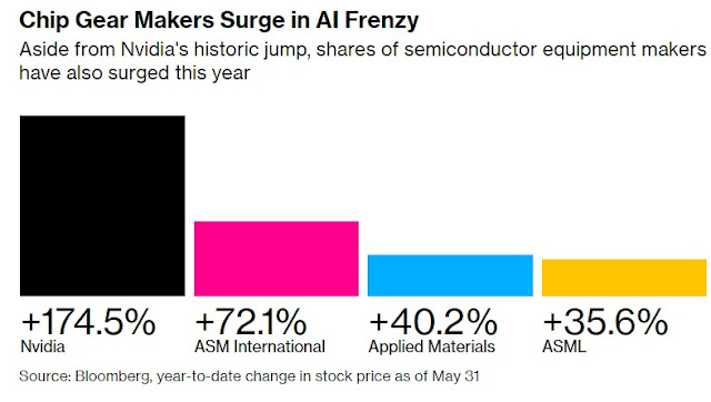
ASM's CEO, Benjamin Loh, highlighted the increasing need for memory in the coming years, particularly in the context of AI technologies. ASM expects the chip market to recover from next year onwards, with sales in 2025 surpassing those of 2022. To capitalize on future growth, ASM plans to invest $100 million in expanding its research operations and facility in South Korea and aims to hire an additional 200 staff within three to five years. Despite restrictions on selling advanced chipmaking gear to China, ASM's position as a key machinery provider to Nvidia, a leading AI accelerator supplier, has contributed to its shares gaining over 70% this year.


Loh, reiterates that the company will experience minimal impact from the restrictions on exporting semiconductor equipment to China. Loh mentions that while they are unable to sell the most advanced equipment, there is still a significant market for other non-restricted equipment, and they can continue trading with Chinese customers. He remains optimistic about the future, stating that as long as chip demand continues to grow, there will be other buyers for their premium products. 

Loh also highlights the challenge of complete decoupling between China and the US, as the chip supply chain remains highly globalized. Recent statements from US officials reflect a shift towards derisking rather than decoupling from China in efforts to improve relations between the two economies.

Thursday, May 18, 2023

ALD/CVD Precursors – Better Times Ahead

Market expected to rebound with memory pricing recovery

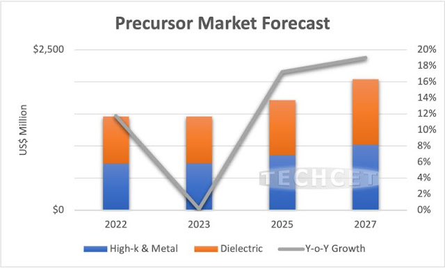
San Diego, CA, May 16, 2023: TECHCET — the electronic materials advisory firm providing business and technology information on semiconductor supply chains — is forecasting semiconductor precursor revenues, both for high-ƙ metal dielectrics and low-ƙ dielectrics, to increase in the 2nd half of 2023, rebounding from the current 0% growth rate. The current market flattening is due to reduced memory pricing in production (DRAM and 3DNAND), as explained in TECHCET’s ALD/CVD Precursors Critical Materials Reports™. In 2027, TECHCET expects the revenues of both the high-ƙ and low-ƙ dielectric precursors to rebound significantly, reaching ~19% growth, as shown in the graph below.


The market is forecasted to also rebound from the current wafer start downturn in 2024. With expansions in 2nm and 3nm logic devices, logic wafer starts below 45nm can reach >7% CAGR in 2027. Additionally, logic growth using more mask layers will drive the demand for metal and dielectric precursors related to patterning and low-k. DRAM is also undergoing a transition to EUV (ALD/CVD hardmasks). Continued scaling of 3DNAND by all global fabricators to above 352-368 layers (using four stacks) continues to move even higher, with expectations of >500 layers by 2030. This also continues to drive the need for dielectric stack deposition, high aspect ratio etch (RIE), and deposition (ALD).

Full implementation of High-k/Metal Gate is driving demand for hafnium precursors as well. This has led to continued supply chain issues for hafnium, especially from major surges in aerospace industry demand. While many other strategic metals and rare earths used for semiconductor production primarily rely on China, hafnium does not. “China currently produces hafnium to satisfy its own demand, and demand from the West is met by production from France, the US, and ongoing expansion in Australian mining operations in the New South Wales Dubbo project,” says Jonas Sundqvist, Senior Technology Analyst at TECHCET.

For more details on the Precursor market segment and growth trajectory, including profiles on suppliers like Adeka, Air Liquide, Entegris, Hansol Chemical, and more, go to: https://techcet.com/product-category/ald-cvd-precursors/

ABOUT TECHCET: TECHCET CA LLC is an advisory services firm expert in market and supply-chain analysis of electronic materials for the semiconductor, display, solar/PV, and LED industries. TECHCET offers consulting, subscription service, and reports, including the Critical Materials Council (CMC) of semiconductor fabricators and Data Subscription Service (DSS). For additional information, please contact info@cmcfabs.org, +1-480-332-8336, or go to www.techcet.com.

Friday, May 12, 2023

Assessing the Environmental Impact of Atomic Layer Deposition (ALD) Processes and Pathways to Lower It

ALD is mainly deployed in high-volume manufacturing in two industrial segments - semiconductor manufacturing and photovoltaics and specifically silicon-based solar cells. Other applications exist but do not yet use anywhere near the amount of processing equipment or plants or electrical energy, gases, chemicals, cooling, ventilation, and clean water. This is why it is important to understand the environmental footprint of ALD in those two industries as a whole and also the contribution from ALD. Here is a good paper breaking down the issues in a systematic way and coming up with some conclusions - three main routes to lower the environmental footprint of ALD.

Assessing the Environmental Impact of Atomic Layer Deposition (ALD) Processes and Pathways to Lower It

Matthieu Weber*, Nils Boysen, Octavio Graniel, Abderrahime Sekkat, Christian Dussarrat, Paulo Wiff, Anjana Devi, and David Muñoz-Rojas
ACS Mater. Au 2023, XXXX, XXX, XXX-XXX
Publication Date:April 27, 2023
https://doi.org/10.1021/acsmaterialsau.3c00002


Due to concerns on resources depletion, climate change, and overall pollution, the quest toward more sustainable processes is becoming crucial. Atomic layer deposition (ALD) is a versatile technology, allowing for the precise coating of challenging substrates with a nanometer control over thickness. Due to its unique ability to nanoengineer interfaces and surfaces, ALD is widely used in many applications. Although the ALD technique offers the potential to tackle environmental challenges, in particular, considerations regarding the sustainability of renewable energy devices urge for greater efficiency and lower carbon footprint. Indeed, the process itself has currently a consequential impact on the environment, which should ideally be reduced as the technique is implemented in a wider range of products and applications. This paper reviews the studies carried out on the assessment of the environmental impact of ALD and summarizes the main results reported in the literature. Next, the principles of green chemistry are discussed, considering the specificities of the ALD process. This work also suggests future pathways to reduce the ALD environmental impact; in particular, the optimization of the reactor and processing parameters, the use of high throughput processes such as spatial ALD (SALD), and the chemical design of greener precursors are proposed as efficient routes to improve ALD sustainability.


Based on the literature review and the green principles applied to ALD depicted in this work, three main routes toward ALD processes with lower environmental impact could be deduced and should be applied where possible:
  1. The thorough optimization of the processing parameters and the reactor design and its infrastructure would drastically lower the undesired wastes and emissions. Computational simulations, machine learning, and artificial intelligence can, for example, be applied to optimize ALD processes faster than ever, as the saturation times can be precisely predicted using these innovative tools.
  2. High throughput processes such as SALD applied at atmospheric pressure could lead to depositions that are orders of magnitude faster and lower the overall energy budget and related emissions.
  3. The chemical design of greener precursors would have the largest impact as it could reduce the overall environmental impact: from the raw material extracted and the (limited) number of greener chemistry synthetic steps resulting in the precursor molecules to the thermal budget related to the deposition temperature, and to the emissions of less polluting byproducts.

Friday, May 5, 2023

INFICON xParts ALD Coatings using Picosun P1000

Inficon's xParts coating service for coating on 3D parts for use in extreme harsh applications such as semiconductor production processes.

In the todays high-tech industries such as the Semi Conductor production, the complexity of the processes and the equipment exposure to harsh chemistry is intense. The desire for tool up-time, high yield and good wafers by lowering the cost of ownership is eminent. Through INFICON xParts ALD coatings one can address exactly these challenges.

1. High conformity allows to coat highly complex 3D geometries with large aspect ratios

2. Outstanding chemical resistance against harsh chemistries (Fluorine, Chlorine etc.)

3. Sealing pores, cracks and voids in thick but porous coatings (E.g Plasma spray)

4. Reduces AlF3 formation and delimitation

Check out the Picosun P1000 in action in the video below.


--------------------------
By Abhishek Thakur

Wednesday, May 3, 2023

AVS ALD2023 & ALE2023 Late News Abstracts Due May 5 - May The 4th Be With You!


Technical Program

Late News Abstracts Due May 5


Hotel Deadline:

June 29


Early Registration:

June 1


The AVS 23rd International Conference on Atomic Layer Deposition (ALD 2023) featuring the 10th International Atomic Layer Etching Workshop (ALE 2023) will be a three-day meeting dedicated to the science and technology of atomic layer controlled deposition of thin films and atomic layer etching. Since 2001, the ALD conference has been held alternately in the United States, Europe and Asia, allowing fruitful exchange of ideas, know-how and practices between scientists.


The conference will take place Sunday, July 23-Wednesday, July 26, 2023, at the Hyatt Regency Bellevue in Bellevue, Washington (East Seattle). As in past conferences, the meeting will be preceded (Sunday, July 23) by one day of tutorials and a welcome reception. Sessions will take place (Monday-Wednesday, July 24-26) along with an industry tradeshow. All presentations will be audio-recorded and provided to attendees following the conference (posters will be included as PDFs). Anticipated attendance is 800+.

Late News Abstracts

Due May 5, 2023

Presenters are limited to one oral and one poster presentation. One submission must be to an oral session and one to a poster session. It must be two different abstracts, not the same abstract submitted as both an oral and a poster.


Key Deadlines:

Late Abstract Deadline:

May 5, 2023

Early Registration Deadline: June 1, 2023

Hotel Reservation Deadline: June 29, 2023

Manuscript Deadline: November 1, 2023


ALD Plenary Speaker

Markku Leskelä

(University of Helsinki, Finland)


ALE Plenary Speaker

Tristan Tronic

(Intel, USA)


ALD Program Chairs


Program Chair:

Seán Barry

(Carleton University, Canada)


Program Co-Chair:

Scott Clendenning

(Intel, USA)

ALE Program Chairs


Program Chair:

Jane Chang

(University of California,

Los Angeles, USA)


Program Co-Chair:

Steve George

(University of Colorado at Boulder, USA)


Program Co-Chair:

Thorsten Lill

(Lam Research, USA)

Forge Nano Partners with Aleon Renewable Metals for Battery Recycling and Supply of ALD Materials for EV Batteries

DENVER , May 2, 2023 /PRNewswire/ -- Forge Nano, a global leader in surface engineering and precision nano-coating technology, and Aleon Renewable Metals (ARM), an integrated lithium-ion battery recycler, announced a partnership today for battery recycling and supply of battery materials. Aleon Renewable Metals will recycle Forge Nano's battery scrap at its industry-leading battery recycling facilities in Texas and Oklahoma utilizing Forge Nano's technology to manufacture cathode active materials (CAM) from the battery grade materials produced by ARM. These facilities aim to make battery recycling easier and more cost effective while outputting leading CAMs made in the U.S. using Forge Nano's proprietary Atomic Layer Deposition (ALD) coating technology, Atomic Armor™. Batteries made with Atomic Armor are optimized to be longer-lasting and safer than current batteries on the market. ARM's facility is expected to annually produce battery grade materials equivalent to 35 GWh of renewable power.


Approximately three billion batteries are thrown away every year in America alone, posing environmental and economical threats far beyond the lifetime of the battery itself. Until now, few companies have addressed the challenges of recycling lithium-ion battery materials. Together, Forge Nano and Aleon are bringing over four decades of combined experience aiming to make E-waste a thing of the past with a 100% renewable energy process.

"In partnership with Aleon Renewable Metals, our technology will be used to provide sustainable and significant cost and performance advantages over competing recyclers making CAMs," said James Trevey , CTO, Forge Nano. "With the cost and performance benefits enabled by Atomic Armor, implementation of this U.S.-born nano-coating technology into the battery-recycling loop embodies the leapfrog improvement in technological advancement everyone has been waiting for in the lithium-ion battery industry."

"We are dedicated to driving sustainability and innovation. Aleon Renewable Metals leverages our proprietary recycling technologies to support the global transition to circular supply chains and cleaner energy. Our high-purity, cost-competitive battery grade materials are positioned to meet the growing domestic demands of the EV market for metal sulfates and lithium compounds used in high-performance cathodes," said Tarun Bhatt , CEO of Aleon Renewable Metals. "With our experience in metal recovery and commitment to sustainable solutions, we are excited to partner with Forge Nano to develop downstream cathode active materials. Together, we will address the projected lithium, nickel, and cobalt supply/demand deficits to create a more attractive environment for sustainable energy production."

As active members of NAATBatt and the MPSC , both companies have demonstrated their dedication to a sustainable battery ecosystem, and their commitment to making a difference in the battery waste problem. This exciting partnership will bring together two world-renowned battery powerhouses in the hopes of taking battery recycling technology to the next level.

"Particle coatings in the field of battery technology are an enabler to excel in the marketplace, which Forge Nano is doing as the global leader in ALD methods to achieve the essential coating characteristics," said Bob Galyen , energy storage technology expert and chairman of Galyen Energy. "The U.S. battery supply chain depends on this kind of innovation to compete on the world stage."

Tuesday, May 2, 2023

TechInsights found Samsung DRAM chips in Samsung Galaxy S23 with Five EUV mask layers

TechInsights found Samsung DRAM chips in Samsung Galaxy S23 with Five EUV mask layers. These are from DRAM wafers produced in the so-called D1a node (or D1α, α as in alpha)


This is in line with a previous press release from Samsung (2020) so no real surprise here: Samsung Announces Industry’s First EUV DRAM with Shipment of First Million Modules – Samsung Global Newsroom

"EUV to be fully deployed from 4th-gen 10nm-class DRAM (D1a) next year"

EUV will be fully deployed in Samsung’s future generations of DRAM, starting with its fourth-generation 10nm-class (D1a) or the highly-advanced 14nm-class, DRAM. Samsung expects to begin volume production of D1a-based DDR5 and LPDDR5 next year, which would double manufacturing productivity of the 12-inch D1x wafers.


Global Semiconductor Sales Decrease 8.7% in First Quarter; March Sales Tick Up Month-to-Month for First Time Since May 2022

Semiconductor sales continued to slip during the first quarter of 2023 due to market cyclicality and macroeconomic headwinds, but month-to-month sales were up in March for the first time in nearly a year, providing optimism for a rebound in the months ahead.

WASHINGTON—May 1, 2023—The Semiconductor Industry Association (SIA) today announced worldwide sales of semiconductors totaled $119.5 billion during the first quarter of 2023, a decrease of 8.7% compared to the fourth quarter of 2022 and 21.3% less than the first quarter of 2022. Sales for the month of March 2023 increased 0.3% compared to February 2023. Monthly sales are compiled by the World Semiconductor Trade Statistics (WSTS) organization and represent a three-month moving average. SIA represents 99% of the U.S. semiconductor industry by revenue and nearly two-thirds of non-U.S. chip firms.


“Semiconductor sales continued to slip during the first quarter of 2023 due to market cyclicality and macroeconomic headwinds, but month-to-month sales were up in March for the first time in nearly a year, providing optimism for a rebound in the months ahead,” said John Neuffer, SIA president and CEO.

Regionally, month-to-month sales increased in Europe (2.7%), Asia Pacific/All Other (2.6%), and China (1.2%), but decreased in Japan (-1.1%) and the Americas (-3.5%). Year-to-year sales decreased across all regions: Europe (-0.7%), Japan (-1.3%), the Americas (-16.4%), Asia Pacific/All Other (-22.2%), and China (-34.1%).

For comprehensive monthly semiconductor sales data and detailed WSTS forecasts, consider purchasing the WSTS Subscription Package. For detailed historical information about the global semiconductor industry and market, consider ordering the SIA Databook.