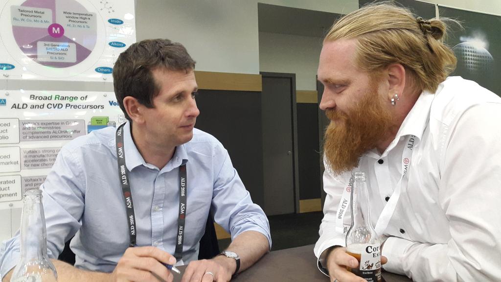
Saturday, July 30, 2016

Winners of the ALD2016 Twitter competition - The #ALDToughGirls

Prof. Henrik Pedersen from Linköping university in Sweden won the Twitter competition at ALD2016. He tweeded actively and managed to cover all aspects of the conference - Scientiffically and Socially and personal funny observations. He also made the innoficial #ALDToughGuys vs. #ALDToughGirls competition go to the girls this time. Maybe ALD2017 will have mixed teams #ALDToughScientists instead?


Photos from ALD.com and Twitter.com

Honor should also go to Miia Mäntymäki for being the first Tough Girl on twitter. Later she enjoyed GTs with the toughest of all ALD Scientists, Tero Pilvi from Picosun at the Airport. He can chew gum and talk Swedish at the same time - it is a self-limmited process.

Photo from Tero Pilvi at facebook.com, the moment just before starting to talk Swedish...

Pico Party (twitter.com)

Some asorted looser ALD Tough Guys below:


Pictures from Twitter.com #ALDToughGuys

Wayne State presented new ALD chemistries for low temperature tantalum and selective cobalt at ALD2016

Prof. Chuck Winter and his team at Wayne State presented new ALD chemistries for low temperature tantalum and selective cobalt at ALD 2016 Ireland this week. Both processes are very important for todays scaling of logic and memory technologies. Metallic tantalum can be used in workfunction engineering of HKMG high performance FinFET transitors as well as for Cu seed/barrier technology in BEOL. Cobalt is as tantantlum an option for Cu barrier/seed and also used selectivly to cap the Cu lines and vias from oxidising and reducing RC performance.


The best highlight talk went to Marissa Kerrigan from Wayne State as voted by attendees on novel Co recursor chemistry for selective Cobalt (Left Marissa Kerrigan, right Simon Elliott, photo by ALD2016.com).

“This opens up the prospect of using tantalum in layers just a few nanometers thick as the liner for interconnect wiring in the complex geometries of next-generation electronic chips,” said the University, which worked with German chemicals giant BASF on the project accoring to Electronic Weekly.

Marissa Kerrigan also from Wayne State announced novel ALD chemistry for metallic cobalt that showed excellent selectivity to copper (photo by ALD2016.com).

“The Wayne State processes for tantalum and cobalt are significant steps forward in controlled growth of ultra-thin metals,” said conference chair, Dr Simon Elliott of Ireland’s Tyndall National Institute. “Strong growth is projected for area-selective deposition: in the near future, it will allow higher-precision patterning of semiconductor chips, and in the longer term it will be an enabler for manufacturing nano-structured materials on demand.” according to the same article in Electronics Weekly.

ALD History Blog: ALD history at ALD 2016 Ireland

ALD History Blog: ALD history at ALD 2016 Ireland: Prof Greg Parsons introducing Prof Anatoly Malygin to give a plenary talk at ALD 2016. Photo by Riikka Puurunen. The  ALD 2016  confer...

Friday, July 29, 2016

A breakthrough in Spatial ALD by Dutch research team at HOLST Centre presented at ALD2016 Ireland

A breakthrough materials processing technique devised by a Dutch research team could lead the way for a new generation of smart fabrics, wearable electronics, solar cells and flat-panel displays.

Many of these technologies work by sandwiching together layers of different materials, with some layers ten thousand times thinner than a sheet of paper (just a few nanometres). Such thin layers can be laid down by a technique called atomic layer deposition (ALD), which is the subject of the new research by Holst Centre/TNO in the Netherlands. Improving how the thin layers are deposited is opening up many new opportunities and applications for flexible electronics in everyday life.

ALD is a highly precise technique for the growth of thin material layers. It is primarily used in the fabrication of electronic chips for an array of consumer products such as PCs, tablets and smartphones. Ultra-thin ALD layers in these devices deliver improved speed, energy efficiency, resolution and memory capacity.

The ALD processes used in the semiconductor industry are precise but slow, depositing roughly one nanometre per minute, and must be carried out in specialised vacuum equipment at low pressure on rigid materials. This is acceptable for making chips in the semiconductor industry, but is an obstacle towards using ALD for coating fabrics, foils or TV displays in a standard factory environment. 

 The research team at Holst Centre/TNO, led by Dr Paul Poodt, has successfully brought ALD out of the vacuum to atmospheric pressure, and shortened deposition times to nanometres per second, without compromising on quality. They achieved this by switching to ‘Spatial ALD’ on large-area and roll-to-roll factory equipment that is suitable for coating flexible films and large sheets. (Picture from LinkedIn.com)

The new technique is one of a number of thin film innovations being presented at the 16th International Conference on Atomic Layer Deposition (ALD 2016), which takes place in the Convention Centre Dublin, Ireland on July 24-27.

The team at Holst Centre/TNO started research into Spatial ALD in 2009 and have successfully shown its use in many applications, including a higher efficiency solar cell that is now on the market. Their current goal of coating porous materials and polymers is even more challenging, but could be hugely rewarding.

Paul Poodt, Program Manager at the Open Innovation Institute Holst Centre said: “We needed to understand the role played by gas pressure in Spatial ALD. Porous materials are like microscopic sponges, and molecules need to travel through all the pores, nooks and crannies before coating the pores properly. We found simple equations that tell us that atmospheric pressure does not in fact slow down ALD in porous materials, but can actually help to speed it up. With this understanding we can make clever designs of new Spatial ALD reactors.”

Dr Poodt added: “We believe that Spatial ALD will make flexible electronics possible soon – useful technologies like foldable displays, wearable phones and smart fabrics. We hope that the results we present at the ALD2016 Conference will be the first step to a new range of applications where Spatial ALD can be a key enabling technology.”

Dr Simon Elliott from Tyndall National Institute, chair of the ALD2016 Conference, said: “This exciting result from TNO is a great example of how seemingly-abstract theoretical understanding of gas flow past obstacles can directly impact on the manufacture of new high-tech devices, such as (O)LED lighting, flexible displays and miniature batteries for wearables.”
Dr Paul Poodt and his team will be presenting their research findings on accelerated growth of thin films onto flexible materials as part of the ALD2016 Conference in Dublin. For further information about the ALD2016 Conference please see http://ald2016.com/


TECHCET Reports Record Silicon Wafer Shipments

TECHCET reports - The silicon demand outlook for 2016 expected to increase of 6.8% to 11.1 BSI, largely due to the strength of the memory market. Regardless of overall wafer consumption, Issues with wafer supply will likely continue, as demand for 300mm polished wafers increases beyond capacity, while epitaxial wafer supply at that diameter remains in excess. Certain 200mm wafers are also in a tight supply situation given strong demand growth from the discrete device fabs coupled with limited supplier capacity, as explained in by Mike Walden, of TECHCET CA. Their recent report further indicates that declining ASPs are expected as competition for China's 200mm wafer demand increases and the 300mm market continues its evolution toward polished wafer usage. 


Although shipments of silicon by area recovered after 2009, prices have still not recovered to 2008 (pre-US housing / WW credit crisis) levels. Silicon area shipments were relatively flat from 2010 through 2013 before rising 10% in 2014. Meanwhile, silicon revenue peaked in 2010-2011 before declining sharply in 2012 and 2013 to begin 4 stagnant years. TECHCET expects aggregate Si ASPs to fall slightly in 2016 before firming or modestly increasing in 2017. Also noted by Walden, "China will have a major influence on this market in the years to come".

For more detailed information and added insight on SOI, China and 450mm wafers, the reader is referred to TECHCET's Critical Materials Report(TM) on the Silicon Wafer Market and Supply Chain.
For more information, please contact info@techcet.com 
or call 1-480-382-8336
 
* Interested in learning more about Membership to the
Critical Materials Council and/or China's supply chain? 
Join the November CMC Meeting in China!

Thursday, July 28, 2016

ASMi ALD Equipment Status & Forecast for growth in 2017

ASM Intertnational released their Q2/2016 report today and here below is the ALD Market Outlook according to ASMi. The Earnings call will be tomorrow so possibly more interesting information will be given then.


  • 2015 has shown a strong growth of the single wafer ALD market. We estimate this growth to continue whereby the single wafer ALD equipment market will double in the period 2015-2018/2019. We however expect the single wafer ALD market to show a double digit decline in 2016, caused by a low demand in Memory which will not be offset by the strong increase in Logic/Foundries. Our single wafer ALD market share is expected to show an increase in 2016. We expect the single wafer ALD market to strongly improve again in 2017.
  • In Memory, the NAND market is shifting from Planar NAND to 3D NAND. This shift will significantly reduce the demand for additional multi patterning-related single wafer ALD capacity. Non-patterning related single wafer ALD demand is expected to gradually increase as soon as next generation 3D NAND is going to ramp into high volume. 
  • In Memory, DRAM industry capacity demand was high in 2015 and has declined strongly in 2016. Based on current visibility the demand for new DRAM-related single wafer ALD capacity is believed to recover earliest in the course of 2017. 
  • In Logic/Foundry the transition to the 10 nm technology node fuels substantially higher single wafer ALD-equipment demand than the previous nodes.

Increasing Demand for Atomic Layer Deposition (ALD) Equipment

Here is a new Market Research report on ALD Equipment from TMR forecasting a continued increase in sales of ALD equipment. This is consistent with other reporting from VLSI Research, Gartner and ASM International. However, this report also claim that export control, lack of ALD experts, and slow dep rate may limit growth. Just returning from ALD 2016 Ireland and the Industry Panel we had there - I do not see that a lack of ALD professionals may be an issue - but who knows maybe that´s the case - so it would be very interesting to know others view on this.

"The absence of skilled human resource and the slow deposition rate of ALD equipment are also likely to curb growth to some extent."


The presence of a large number of international and local companies is boosting competition in the global atomic layer deposition (ALD) equipment market. As per a new study by Transparency Market Research (TMR), the competition prevailing in the market is expected to intensify further between 2016 and 2024. As of 2015, ASM International N.V., Applied Materials, Inc., and Tokyo Electron Ltd. cumulatively held a share of 58.9% in the global market. Of these, ASM International N.V. emerged as the top player, accounting for over 28% of the global ALD equipment market in 2015. Rivalry among key players in terms of product development and technology and product upgrades is expected to intensify during the forecast period.

"Due to the recent advancements in the atomic layer deposition technology, the use of ALD equipment has considerably increased in the nanotechnology sector," says a lead analyst at TMR. TMR expects applications of ALD equipment as manipulation and fabrication tools in nanotechnology to rise further in the short term. "Growing concerns pertaining to carbon emissions have accelerated investment in the R&D of photovoltaics. Due to the increasing research and development activities, the use of ALD as a PV manufacturing method has substantially expanded," adds the analyst. This rising demand for photovoltaic cells, combined with rapid advancements witnessed in PV technology, will subsequently augment sales of ALD equipment in the forthcoming years.

ALD2016 Ireland Photo show

The 16th International Conference on Atomic Layer Deposition (ALD 2016) was a three-day meeting dedicated to the science and technology of atomic layer controlled deposition of thin films. In every year since 2001, the conference has been held alternately in United States, Europe and Asia, allowing fruitful exchange of ideas, know-how and practices between scientists. This year, the ALD conference incorporated the Atomic Layer Etching 2016 Workshop. The conference took place on 24-27 July 2016 at the Convention Centre Dublin, Ireland.

ALD2016 was a grand event and a success! Here I am collecting pictures from the event from Twitter (#ALD2016), The ALD Confernce and others - please send me pictures and I will publish them if you like to share them (jonas.sundqvist@baldengineering.com).


ALD2016 Co-Chairs Simon Elliott (Tyndall National Institute, Ireland) and Jonas Sundqvist (Lund University, Sweden / Fraunhofer IKTS, Germany) taking a final look into the Program before opening the conference on Monday morning. (Picture by ald2016.com)


Opening of ALD2016 by Kieran Drain CEO Tyndall National Institute. (Picture by ald2016.com)


Suvi Haukka from ASM International receiving The ALD Innovation Prize 2016. The prize was presented by last year's awardee Prof. Greg Parsons. (Picture by ald2016.com)


The conference chairs of ALD2016 (Simon Elliott and Jonas Sundqvist) and ALE2016 (Prof. Bert Ellingboe) together with Dennis Hausmann (International & Local Program Committee, Lam Research) learning how to pour a Pint of Gunniess at the Welcome reception that was held at the Guinness Store House in Dublin. (Picture by ald2016.com)

Encapsulix SAS Introduces InfinityTM 200 Atomic Layer Deposition System

SIMIANE-COLLONGUE, France – July 26, 2016 – Encapsulix SAS today introduced its InfinityTM 200 Atomic Layer Deposition (ALD) system product line optimized for deposition onto 200 mm substrates in a manufacturing or R&D environment. The line’s advanced features for nano-engineered materials include a special focus on low temperature, thin-film encapsulation for flexible organic electronics, in particular organic light-emitting diodes (OLED).

The new 200 ALD line incorporates Encapsulix’s proprietary Parallel Precursor Wave (PPW) technology, which deposits atomic-level coatings with unmatched precision and throughput. The system has been successfully installed and qualified for ultrafast OLED encapsulation at Leti, the CEA Tech research institute in Grenoble, France. Additional systems will be delivered in the next 12 months to customers in Asia.

“We are pleased to strengthen our product offering to the OLED industry with this product family. The strategic partnership with Leti, and the successful application of our technology in the most demanding OLED encapsulation applications, confirm our position as the industry leader in ALD for OLED encapsulation,” said Dr. Jacques Kools, founder and CEO of Encapsulix SAS. “Our high-speed ALD thin-film encapsulation technology proves to be a key enabler in the flexible electronics revolution”.


Introduction to Encapsulix introduction, Dr. Jacques Kools, founder and CEO of Encapsulix SAS (Youtube).

“Since its launch in 2011, Encapsulix has continuously improved the performance of high-throughput atomic layer deposition equipment and processes,” said Dr. Tony Maindron, OLED senior scientist and project leader at Leti. “This new, ultrafast InfinityTM 200 system will strengthen Leti’s OLED development projects for next- generation wearable devices and other uses.”

The Infinity ALD equipment platform was developed by Encapsulix to address the microelectronic industry’s need for geometrically scaled nano-engineered coatings. These coatings range from 10-100 nm in thickness, and often are comprised of sublayers with nanometer thickness. The Infinity series provides the unique ability to transfer the process from R&D on 200 mm (resp. generation 2.5) in Infinity 200 (resp. Infinity 500) systems to manufacturing on generation 4.5 and generation 6 substrate sizes in Infinity 750 and Infinity 1000 tools. These capabilities provide a reliable route for quickly ramping the most advanced thin-film encapsulation solutions for flexible AMOLED.

About Encapsulix
Encapsulix was founded to address the geometric scaling of critical deposition requirements for industrial & microelectronic devices and foils. Initial process focus is in Al2O3 and TiO2 specifically for barrier coatings. The company has its development and headquarters in Simiane-Collongue France, equipment development, sales and service in the USA.

For more information:
Contact: www.encapsulix.com
Europe : Jacques Kools jkools@encapsulix.com

Friday, July 22, 2016

KAUST showcase Indium-Free Fully Transparent Electronics Deposited Entirely by ALD

Materials Science and Engineering, King Abdullah University of Science and Technology (KAUST), Thuwal, Saudi Arabia has come up with a process to fabricate Indium-Free Fully Transparent Electronics Deposited Entirely by ALD. Below is the abstract fro the paper published recently in Advanced Materials.

Indium-Free Fully Transparent Electronics Deposited Entirely by Atomic Layer Deposition

Pradipta K. Nayak, Zhenwei Wang and Husam N. Alshareef
Version of Record online: 4 JUL 2016


Abstract:


Indium-free, fully transparent thin-film transistors are fabricated entirely by atomic layer deposition technique on rigid and flexible substrates at a low temperature of 160 °C. The transistors show high saturation mobility, large switching ratio and small subthreshold swing value. The inverters and ring oscillators show large gain value and small propagation delay time, indicating the potential of this process in transparent electronic devices.

Here is the ALD process flow for a fully transparent TFT display published accordingly in the Supporting Information that is free for download.


Incom is looking for the best and brightest ALD talent


ALD Research Scientist

Incom, Inc., headquartered in Charlton, Massachusetts (USA), is looking for the best and brightest ALD talent with both practical, hands on experience and appropriate technical understanding to operate and develop Atomic Layer Deposition (ALD) processes and to support commercialization of Incom Microchannel Plates (MCP) and related ALD coated products.


Reporting to the Director of R&D, the ALD Research Scientist will be responsible for the functionalization of MCPs, in collaboration with R&D team members. The ALD Research Scientist will be a key contributor toward business development and commercialization of Incom’s MCP product line.
Responsibilities:
·         Work as an integral member of the R&D team, with responsibility for all facets of ALD processing, working directly with Incom’s ALD R&D Scientist
·         ALD process qualification and optimization for functionalization of MCPs
·         Analyze ALD films using thin film characterization techniques
·         Troubleshoot ALD system, schedule and facilitate maintenance of system
·         Document ALD processes, disseminate results and create SOPs for Incom’s manufacturing personnel
·         Interface with prospective customers to understand their technical requirements and to ensure that prototype samples are specified and fabricated appropriately.
Qualifications
·         BA, BS, Masters (with 3-7 years of industry experience), or Ph.D. degree (with 0-5 years of experience) in Chemistry, Physics, Materials Science, or Chemical Engineering required.
·         Technical background and hands on, practical experience with ALD system operation, process optimization and troubleshooting is essential.
·         3-5 years of experience with thin film characterization (ellipsometry, electrical characterization, SEM, surface spectroscopies etc.) is required.
·         3-5 years of demonstrated productive track record in related research and/or development.
·         Experience working in a cleanroom work environment is preferred.
·         Occasional travel to Argonne National Lab to complete ALD processing of MCPs is required.
·         English fluency (speaking, comprehension, reading and writing) is required for effective performance in this position.
·         Excellent verbal and written communication skills.
·         Essential Competencies: Initiative, creativity, integrity, accountability, collaboration and teamwork.
Come work with us in a fast paced environment where you will be empowered and included, where innovation is encouraged and everyone’s voice can be heard. At Incom, high performing individuals have the opportunity to grow professionally, and develop rewarding careers. Incom offers a competitive compensation and benefits program.

NOTE: Incom will not sponsor individuals for employment visas, now or in the future, for this position. Applicants for employment must be able to meet access requirements to work on-site at the Argonne National Laboratory.

Incom is an Equal Opportunity and Affirmative Action Employer, including Veterans and Individuals with Disabilities.

To apply visit our website: www.incomusa.com      

How to get the ALD2016 Ireland Conference App

Before you get on the flight to Ireland you should tak a moment to download teh excellent Conference App that will give you access to the complete program and all abstracts. It is a convienient guide to the conference program and you can write your own notes.


Here is a direct link for :


Lund Nano Lab to present new maskless technology for nano device patterning at ALE 2016 Ireland

Semiconductor device scaling requires atomic level precision processing and Atomic Layer Etching (ALE) has a great potential for this. ALE is a cyclic etching process in which a well-defined atomically thin layer is etched in each cycle. [HERALD White Paper on Atomic Level Processing]

Lund Nano Lab at NanoLund, Lund University to present new maskless technology for nano device patterning at ALE 2016 Ireland. Here you can have a preview and we welcome all of you to enjoy the opening pleanary talk by Prof. Lars Samuelson and later the contributed talk by Dr. Dmitry Suyatin in the ALE Workshop. Later you may also want to come and stop by and visit us in the Exhibition at the joint stand NanoLund and ALD Lab Saxony - table 45 right next to the coffee.

Nanowire-based Technologies for Electronics, LEDs and Solar-cells
Lars Samuelson
Lund University, Sweden
08:30-09:00


Dr. Dmitry Suyatin from Lund university presenting initial groundbreaking work on splitting Nanowires by ALE at the Novel High-k Workshop in Dresden 2016. At ALE 2016 more details will be revealed.


Longitudinal nanowire splitting by atomic layer etching
DMITRY B. SUYATIN*, MD SABBIR AHMED KHAN, JONAS SUNDQVIST, ANDERS KVENNEFORS, MARIUSZ GRACZYK, NICKLAS NILSSON, IVAN MAXIMOV
Lund University, Sweden
13:45-14:00


Invention

We provide an ALE-based maskless method of manufacturing nanostructures with characteristic size below 20 nm

Offer

  • IP & licencing 
  • ALE Process development 
  • Device fabrication 
  • Process transfer

Beneq strengthens its lead in high-volume industrial ALD

20 July 2016, Beneq, a leading supplier of ALD equipment and thin film coating services, today announced two new thin film equipment solutions for industrial customers that require high capacity and low process cost in advanced ALD applications. The new products are set to revolutionize the standards of coating speed in the ALD industry.

Beneq R11™ – Ultra-fast high precision spatial ALD coating

Beneq R11 is the latest addition to Beneq’s extensive portfolio of large-throughput spatial ALD solutions for industrial use. It provides an optimal solution for high performance ALD on wafers in industrial applications, such as optical coatings, insulators and barriers. It is the ideal choice of equipment when speed, cost, low process temperature and the highest possible film quality are the driving factors.

With Beneq R11, it is for the first time possible to use PEALD (Plasma Enhanced ALD) processes in high volume manufacturing. The system lends itself to barrier, insulation and anti-corrosion applications for MEMS, LED, OLED, photovoltaics, high power semiconductors, sensors and many other components.

The equipment is suitable for up to 200 mm wafers and other round or rectangular substrates. The plasma enhanced rotary ALD process of Beneq R11 is ideal for thick ALD films, in the micrometer thickness range. Beneq R11 can also be equipped with standard wafer automation.


Beneq T2S™ – Automated batch wafer equipment

Beneq T2S is the newest member of Beneq’s wafer-based production equipment portfolio. It offers a unique combination of high capacity batch processing and standard cassette-to-cassette automation. The Beneq T2S is specifically engineered to match the semiconductor requirements, including the SEMI S2 safety requirements and low particle counts.

Beneq T2S is perfectly suited for high volume manufacturing in various wafer-based applications, including MEMS, LED, OLED, ink-jet print heads and more. The thermal batch ALD process of Beneq T2S is ideal for oxide and nitride processes used for dielectric, conductor, barrier and passivation purposes.

The equipment is designed for wafers up to 200mm in diameter and can process 25 wafers per run in face-down or face-up orientation.

New products officially unveiled in ALD2016 in Dublin, Ireland

Both new products, Beneq R11 and Beneq T2S, will be introduced officially for the first time next week at ALD2016 – the 16th International Conference on Atomic Layer Deposition, which will be held at the Convention Centre Dublin, Ireland, 24-27, July 2016. Beneq is a platinum sponsor of the event.

Says Tommi Vainio, Vice President, Thin Film Equipment, at Beneq: “High capacity industrial ALD solutions are an important and expanding part of our product portfolio. Our commitment to revolutionize the coating speed standards in the ALD industry is clearly demonstrated in the new ALD equipment we are launching in Dublin. From now on with Beneq, the unit for ALD area is m2 instead of mm2.”

More information about the new products and the multitude of Beneq ALD applications is available at the Beneq stand in the ALD exhibition of the conference. The number of the Beneq booth is 30. You can also visit Beneq Monday through Wednesday at the Beneq Boat Bar right next to the convention centre.

Strem Chemicals Inc. as a new sponsor of the BALD Engineering ALD Blog

I am very happy to announce Strem Chemicals Inc. as a new sponsor of the BALD Engineering ALD Blog! Please take a moment wo check out their dedicated page and extensive offering of ALD & CVD Precursors as well as Bubblers and Cylinders:

http://www.strem.com/bald


RASIRC Presents Two New Molecules for Growth of Low Temperature Nitrides and Oxides

BRUTE gases improve passivation and nucleation for High k Deposition in ALD

San Diego, Calif – July 21, 2016 – RASIRC will demonstrate continued technology leadership in gas delivery for new semiconductor materials and processes with a presentation, posters and exhibit (stand #48) at the 16th International Conference on Atomic Layer Deposition July 24-27 in Dublin, Ireland. The company will discuss how anhydrous hydrogen peroxide and hydrazine can improve key processes and will present initial electrical characterization data for films and MOSCAP structures.
Presentation

 RASIRC Chief Technology Officer Dan Alvarez will present “Novel anhydrous hydrazine deliver for low temperature silicon nitride passivation of SiGe(110)” on Monday July 25 in the Precursor Delivery session. This presentation will discuss how anhydrous hydrazine can be used to create a thin layer of silicon nitride that can act as a diffusion barrier or channel passivation layer prior to dielectric deposition in FinFets or MOSFETs. The study focuses on <400C silicon nitride ALD process and shows how further oxidation using anhydrous peroxide provides good nucleation for High k deposition.
 
“Anhydrous hydrazine gas offers a new path to low temperature passivation and nitridation,” said Alvarez. “This highly reactive molecule shows a higher growth rate, density and reactivity when compared to other plasma free chemistries.”
Poster Session

RASIRC will present the poster “Hydrogen peroxide gas for improved nucleation and initiation in ALD” on Monday July 25 in Joint Poster Session 1. The poster explains the need for a novel oxidant that improves passivation and nucleation density at semiconductor interfaces. The study was performed on SiGe(110) surfaces and provides a direct comparison of equal amounts of water, 30% H2O2/H2O, and anhydrous H2O2. A five-fold increase was found in nucleation density for H2O2 versus water, and a three-fold increase for H2O2 versus 30% H2O2/H2O. An additional comparison was made of H2O2 to H2O by deposition of Al2O3 on an Si-H surface. This comparison found denser nucleation and faster initiation for H2O2 treated surfaces.

Also during Joint Poster Session 1, Karl Littau of Intermolecular, USA, will present a poster that stems from work done using RASIRC anhydrous hydrogen peroxide. His poster titled “Comparison of hydrogen peroxide and ozone for use in zirconium oxide atomic layer deposition” includes Dan Alvarez and Jeff Spiegelman as co-authors. The study compared RASIRC BRUTE™ Hydrogen Peroxide and ozone as oxidants for zirconium oxide ALD. The effects of the oxidants on ZrOx growth rate, film composition, crystallography and metal-insulator-metal capacitor dielectric constant and leakage are discussed.

“Results from multiple studies performed at university labs and customer sites have repeatedly shown that anhydrous hydrogen peroxide delivers better surface functionalization and initiation than either water or 30% H2O2/H2O,” said Jeffrey Spiegelman, RASIRC President and Founder. “New materials require new gases, and RASIRC is leading the way through innovative new molecules and gas delivery systems.”
Exhibit Stand

ALD Conference attendees are invited to visit RASIRC in booth #48. Representatives will be available to answer any questions and discuss exciting results from recent customer testing. Stop by to get the latest research papers and see a demonstration model of our unique solvent-based delivery system for safety, used for BRUTE Hydrogen Peroxide and BRUTE Hydrazine. Also learn about the Peroxidizer® for high-volume ALD. Ask about Hydrogen Peroxide Steam.


Thursday, July 21, 2016

Signed the contract to supply ALD equipment to Chinese DMEGC for high efficiency solar cells

NCD has just contracted with Chinese DMEGC to supply solar cell manufacturing equipment which would produces over 100MW. This equipment is Lucida GS Series ALD system for mass-producing high efficiency crystalline solar cell using Al2O3-ALD passivation to reduce surface defects on the rear side of wafers. This is paramount achievement because it is export of mass production equipment to China of the Mecca of solar cell production through winning against big international competitors. The production capability of this equipment has been improved through our a lot of production experience comparing to the previous systems. It certainly shows that the customer has proved the technology of NCD and the excellence of the equipment, and NCD would make it the most memorable turning point for our future oversea sales.

Lucida™ GS Series ALD
High throughput atomic layer deposition system for surface passivation of c-Si solar cells


Lucida™ GS series

Lucida™ GS series + Automation


Applications
·         Al2O3 surface passivation of c-Silicon solar cells
·         Applications of mass-production
·         Industrial fully-automated production equipment
·         High throughput : up to 3400 wafers/hour of 156 x 156
Features
·         Al2O3 thin films with good thickness uniformity
·         Advanced process kit and small volume chamber for short gas cycle times
·         Extremely materialize ALD mechanism
·         Small foot print
·         Totally integrated process module
·         Easy process control
·         Automatic cassette to cassette operation
Technical specifications

Model
Material
Wafer size
(mm2)
Thickness
(nm)
Throughput
(wph)
Lucida™ GS800
Al2O3
156x156
10
>1700
Lucida™ GS1200
Al2O3
156x156
10
>2400
Lucida™ GS1600
Al2O3
156x156
10
>3400