Showing posts with label Spatial ALD. Show all posts

Thursday, April 30, 2015

Pneumatic flow reactor for continuous production

Here is a very interesting new Spatial ALD Technology for coating particles - Delft IMP.

"Delft IMP (Intensified Materials Production) commercializes nanostructuring of particles using atomic and molecular layer deposition (ALD and MLD), based on the patented and publicized IP and know-how developed within the Product & Process Engineering (PPE) group at Delft University of Technology. Following various feasibility projects between industry and university, Delft IMP was initiated end 2014 to truly commercialize the technology."

Pneumatic flow reactor for continuous production 
 
"For catalysis, required volumes are much higher, and stringent product control over the entire production is needed. For this purpose, Delft IMP and Technical University of Delft have developed a new patent protected reactor concept, a based on pneumatic transport, as shown in figure below."

ALD scale-up

Schematic of ALD in a pneumatic transport reactor. Check out the company web from more details here

Tuesday, April 7, 2015

A spatial ALD oxide passivation module in an all-spatial etch-passivation cluster concept!

Prof. Fred Roozeboom and co-workers F. van den Bruele, Y. Creyghton, P. Poodt, and Prof. W.M.M. Kessels (all from Eindhoven University of Technology and TNO, as driving forces behind Spatial ALD and ALE technology), have just published a fantastic open access publication in ECS Journal of Solid State Science and Technology. Just taste the title of this blog text for a moment and then continue reading or down load the article - it´s free, it´s OPEN ACCESS.

Cyclic etch /passivation-deposition as an all-spatial concept towards high-rate room temperature Atomic Layer Etching [OPEN ACCESS]
F. Roozeboom, F. van den Bruele, Y. Creyghton, P. Poodt, and W.M.M. Kessels
ECS Journal of Solid State Science and Technology, 4 (6) pp. N5067-N5076 (2015). doi:10.1149/2.0111506jss

Conventional (3D) etching in silicon is often based on the ‘Bosch’ plasma etch with alternating half-cycles of a directional Si-etch and a fluorocarbon polymer passivation. Also shallow feature etching is often based on cycled processing. Likewise, ALD is time-multiplexed, with the extra benefit of half-reactions being self-limiting, thus enabling layer-by-layer growth in a cyclic process. To speed up growth rate, spatial ALD has been successfully commercialized for large-scale and high-rate 
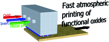
deposition at atmospheric pressure. We conceived a similar spatially-divided etch concept for (high-rate) Atomic Layer Etching (ALEt). The process is converted from time-divided into spatially-divided by inserting inert gas-bearing ‘curtains’ that confine the reactive gases to individual injection slots in a gas injector head. By reciprocating substrates back and forth under such head one can realize the alternate etching/passivation-deposition cycles at optimized local pressures, without idle times needed for switching pressure or purging. Another improvement toward an all-spatial approach is the use of ALD-based oxide (Al2O3, SiO2, etc.) as passivation during, or gap-fill after etching. This approach, called spatial ALD-enabled RIE, has industrial potential in cost-effective back-end-of-line and front-end-of-line processing, especially in patterning structures requiring minimum interface, line edge and fin sidewall roughness (i.e., atomic-scale fidelity with selective removal of atoms and retention of sharp corners). 

The publication starts with a History of 3D etching and a description of how and why plasma etching is a key enabling technology and then it gets down to business to introduce the concept behind layer-by layer growth (ALD) or etch (ALE) and more importantly the concept behind spatial layer-by-layer processing. Then via the cyclic Bosch process, and Spatial RIE with Spatial passivation we land at the Grand Finale - Spatial RIE process mode with Spatial ALD passivation!  Or even more beautifully formulated by Prof. Roozeboom himself a spatial ALD oxide passivation module in an all-spatial etch-passivation cluster concept!


Layer-by layer-processing
Figure 3.

Schematic of conventional CVD and plasma etching and their layer-by-layer counterparts, ALD and ALEt. ALEt is cycled between modification by chemisorption of a reactant at the surface and, subsequent volatilization of, ideally, one (sub)monolayer by irradiation with an energetic beam or reaction with a co-reactant. For simplicity reasons the etch processes (bottom pictures) are cartooned in plasma-assisted mode, and the deposition processes (top pictures) in thermal mode. The latter two could be plasma-assisted as well. In the conventional processes (CVD and Plasma etch) the chemical reactants are supplied simultaneously and non-interrupted, and in the layer-by-layer processes (ALD and ALEt) they are alternated. (picture used with permission)

Spatial ALD

Figure 4. 

Schematic representation of spatial ALD: a wafer moves horizontally back and forth under spatially divided and confined reaction zones. Arrows pointing upwards indicate exhaust lines. Notice the difference in height of the gas bearing compartments (typically ∼20 to 100 μm) and the deposition compartments (typical height a few mm, and lengths and widths of order ∼1-10 mm).(picture used with permission)

Convential Bosch etching by cyclic surface passivation half-cycles
 
Figure 6. 

Conventional Bosch etch process scheme for etching silicon with a pre-patterned hard mask atop, using alternating etch and passivation half-cycles. (picture used with permission)

Spatial RIE process mode with C4F8 passivation

Figure 7.

Schematic of spatial RIE process mode with C4F8 passivation of a wafer that reciprocates under spatially divided reaction zones. Arrows pointing upwards indicate exhaust lines. Notice the difference in height of the gas bearing compartments (typically ∼20 to 100 μm) and the plasma compartments (typical height ∼10 mm, and length of several 10 mm's and width of order ∼1 mm). The compartments are connected through a gas bearing envelope. Not to scale; wafers will pass the entire zones before shuttling back.  (picture used with permission)

Spatial ALD oxide passivation module in an all-spatial etch-passivation cluster concept

Figure 8. 

Schematic of alternative all-spatial RIE process mode with spatial ALD oxide passivation (e.g., SiO2, Al2O3, ..). ‘Si’ denotes a Si-precursor, TMA is trimethyl aluminum. Note, that for deep etching and for shallow (‘layer-by-layer’) etching the wafer exposure times in the respective zones will differ, which will imply different residence times, or different numbers of unit cells in the two main compartments.  (picture used with permission)

At the end after showing a number of case studies, Prof. Roozeboom et al summarizes - and we all believers will agree on these conclusions - namely that:
  • The potential of ALD-assisted nanomanufacturing technologies like Atomic Layer Etching (ALEt) concepts derived from etch-purge-passivation/deposition-purge subroutines in (D)RIE and ALD is now clearly being recognized and promoted.
  • The ongoing scaling of Moore's Law will soon require the implemention of these complementary technologies to meet the 10-nm challenges in surface and sidewall passivation of resist and feature patterns that is required to minimize interface, line edge and fin wall roughness.
  • For cost reasons and flexibility in local pressure, i.e. (an)isotropy control, in the spatial etch and purge compartments one can envisage a gradual shift to the adoption of ALD-enabled RIE (we abbreviate it as ALDeRIE) in the spatial domain as well. 
  • Obviously, the spatially divided version is not commercially available yet and not straightforward, but – once realized for dedicated materials and topographies – it will certainly lead to far improved price-performance ratios in Atomic Layer Etching.  

http://www.solliance.eu/uploads/RTEmagicC_DSC_7183_Photo_ECS_Fellow_Oct14.jpg.jpg 

Fred Roozeboom appointed as ECS Fellow, The Electrochemical Society appointed Prof. dr. Fred Roozeboom as Fellow of the Electrochemical Society  for his Scientific contributions to Solid-State Science & Technology and its impact on the society. He has been awarded especially because of his contributions on the areas of rapid thermal processing, passive 3D and heterogeneous integration, reactive ion etching and atomic layer deposition (ALD). He received his award at the Plenary Session of the 226th ECS meeting. October 5, 2014, Cancun, Mexico.
 

Tuesday, March 10, 2015

Spatial ALD at low temperature for flexible electronics encapsulation using a BENEQ R2R

A recent paper on Spatial ALD at low temperature for flexible electronics encapsulation using a BENEQ R2R system at Advanced Surface Technology Research Laboratory Team (ASTRaL), Laboratory of Green Chemistry, Lappeenranta University of Technology, Finland. Thanks Henrik Pedersen for finding this one!

Philipp S. Maydannik, Alexander Plyushch, Mika Sillanpää, and David C. Cameron

Water and oxygen were compared as oxidizing agents for the Al2O3 atomic layer deposition process using spatial atomic layer deposition reactor. The influence of the precursor dose on the deposition rate and refractive index, which was used as a proxy for film density, was measured as a function of residence time, defined as the time which the moving substrate spent within one precursor gas zone. The effect of temperature on the growth characteristics was also measured. The water-based process gave faster deposition rates and higher refractive indices but the ozone process allowed deposition to take place at lower temperatures while still maintaining good film quality. In general, processes based on both oxidation chemistries were able to produce excellent moisture barrier films with water vapor transmission rate levels of 10−4 g/m2 day measured at 38 °C and 90% of relative humidity on polyethylene naphthalate substrates. However, the best result of <5 × 10⁻⁵ was obtained at 100 °C process temperature with water as precursor.


Schematic view of modified SALD TFS200R reactor with drum and N2 and precursor inlet, and exhaust ports. J. Vac. Sci. Technol. A 33, 031603 (2015); http://dx.doi.org/10.1116/1.49140


http://www.beneq.com/sites/default/files/imagecache/pageimage_app/TFS%20200R_chamber_.jpg
Close up inside the drum of the Beneq TFS 200R, which is  designed for research in Roll-to-Roll atomic layer deposition (ALD) and other forms of continuous ALD (CALD). (www.beneq.com)


Information from BENEQ.com: In the TFS 200R, the flexible substrate is fixed on a rotating cylinder within the reaction chamber. The cylinder itself is surrounded by a number of linear nozzles, each creating an isolated gas region over the full width of the substrate. As the cylinder is rotated, the substrate passes through different gas regions and is coated.

The Beneq TFS 200R, with its robust and modular structure, is designed to meet both industrial standards and the flexibility requirements of research today. Precursor containers are conveniently small, and they can be easily changed. Depending on the process needs, the TFS 200R can be equipped with up to 2 heated sources, type HS 80 and/or HS 180. Additionally, the system can be equipped with up to 8 gas lines and up to 4 liquid sources.

http://www.beneq.com/sites/default/files/TFS%20200R%20modattu%20rgb%20120%20copy.jpg

Thursday, February 19, 2015

Veeco has decided to lower its spending rate in FAST-ALD

Veeco's Q4 MOCVD revenue up 55% year-on-year while orders almost triple and during Q4/2014, Veeco successfully demonstrated its FAST-ALD (atomic layer deposition) technology for flexible organic light-emitting diode (OLED) encapsulation at a key customer. However, at the same time, the incumbent deposition technology has progressed to satisfy the current market requirements, and Veeco has not received any sizable orders for OLED encapsulation tools. While this opportunity "may not be permanently off the table", the firm has hence lowered the near-term revenue forecasts for its ALD technology and taken a non-cash asset impairment charge (goodwill, intangibles and property, plant and equipment) of $55m in Q4. Veeco has also decided to lower its spending rate in ALD, refocus R&D efforts on semiconductor and other applications, and continue to monitor the flexible OLED market opportunity.

Beneq WCS 600 Web Coating System for Roll-to-Roll ALD

Beneq has introduced WCS 600, a new coating system based on the roll-to-roll atomic layer deposition (ALD) technique. Designed to suit the different needs of customers, this system has a coating capacity of 400,000m2/yr. It is capable of processing different types of substrate materials of varying thicknesses.

Beneq WCS 600 Web Coating System for Roll-to-Roll ALD
 
The WCS 600 features a vacuum chamber with ALD coating head, processing drum and web reels. The device is operated at temperatures up to 150°C.

The WCS 600 can be easily scaled up from R&D to pilot production for different industrial applications, including buffer layers for CIGS solar cells and moisture barriers for flexible organic electronics.

Key Features

  • The main features of the Beneq WCS 600 web coating system include:
  • True roll-to-roll ALD process
  • Non-contacting web handling
  • Precursor de-activation system
  • Electrical and control cabinet with PC user interface
  • Coating capacity of 400,000m2/yr
  • Maximum web width 600mm

Thursday, January 29, 2015

Levitech BV sells two Levitrack ALD systems to Japanese high-performance solar cell manufacturer

As reported by Levitech BV, a leading supplier of advanced process equipment for the manufacturing of solar cells, announced today that it has sold two Levitrack Atomic Layer Deposition (ALD) systems to Japan, the first multiple system order for ALD equipment in the world. A major multinational, which includes solar cell manufacturing among its many concerns, will use the Levitracks for high-volume production and the development of next-generation, high-efficiency crystalline solar cells.

ald cycle 350px

“The further success of the Levitrack, with two being sold to a prestigious client, is confirmation that our mass production solutions for fast ALD deposition deliver the right product to meet the needs of mass-production manufacturers”, stated Jaap Beijersbergen, CEO of Levitech. “The system will be used for PERC cells - with efficiencies exceeding 20 per cent - as well as multi-crystalline and n-type products.”

Since its introduction in 2010, the Levitrack has consistently demonstrated its advanced passivation capabilities at world-leading manufacturers and institutes in both Europe and Asia.
“We know that aluminum oxide film provides excellent cell passivation and increased cell efficiencies, especially when deposited in uniform and dense layers, a particular feature of the ALD technique. In the Levitrack these qualities are combined with an efficient and effective platform for delivery,” said Beijersbergen.

“This customer chose the Levitrack system based on its significant productivity, cost-of- ownership and process advantages over competitive PECVD and other ALD systems for aluminum oxide (Al2O3) applications.”

Wednesday, January 14, 2015

Hanwha Q Cells to evaluate SoLayTec InPassion technology

Dutch research spinoff SoLayTec has announced that Hanwha Q Cells has begun evaluating its atomic layer deposition (ALD) technology. The InPassion ALD can be deployed for PERC upgrades and n-type cell production.
“Last month in November SoLayTec announced it sold its first production machine in the U.S. for a 100MW n-type bi-facial cell line. Now also Hanwha Q CELLS decided to start the evaluation of the InPassion ALD system from SoLayTec for its high efficiency cell concepts in Thalheim (Germany).”

SoLayTec’s Görtzen says that the company’s goal is to demonstrate that the InPassion ALD process has a higher potential than the plasma-enhanced chemical vapor deposition (PECVD) approach.

“The biggest advantages of our spatial ALD tool compared to PECVD are a better step coverage, a stable uniformity and a layer thickness requirement of only 5 nm Al2O3,” said Görtzen. “Furthermore, if in the ALD cell process flow a direct PECVD is used for the SiN capping layer an integrated annealing process can be implemented, resulting in better cell performance compared to PECVD AlOx.”

Read more: http://www.pv-magazine.com/news/details/beitrag/hanwha-q-cells-to-evaluate-solaytec-inpassion-technology_100017741/#ixzz3OmOeCWkJ

Wednesday, November 26, 2014

SoLayTec Sells Spatial ALD Machine To Mission Solar

As reported by SoLayTec : Texas-based Mission Solar Energy has ordered an InPassion atomic layer deposition (ALD) machine from Netherlands-based SoLayTec for its high-efficiency n-type silicon bifacial solar cell line.

 
Mission Solar recently opened a solar panel manufacturing facility at Brooks City-Base in San Antonio. The 240,000 square-foot facility produces n-type solar cells and 72-cell 320 W modules for Korea-based OCI Co. Ltd., which is developing four large-scale projects in the region, including the Alamo projects for CPS Energy.

SoLayTec says the order is its first U.S. sale.


SoLayTec is a spin-off company from the Dutch research organisation TNO and established in 2010. The company develops, delivers and services machines for atomic layer deposition (ALD) on solar cells worldwide. The SoLayTec ALD machines are intended for industrial production in the solar market. SoLayTec mass production equipment will be exclusively sold together with RENA GmbH on the market. RENA

Tuesday, October 14, 2014

Levitech 5 Year Anniversary - ALD4INDUSTRY Workshop

Levitech will celebrate its 5th Anniversary on Thursday October  30th, 2014 with a Workshop Program and an Anniversary Program  at Levitech in Almere. "For this day Levitech invited several national and international  speakers from the field of Atomic Layer Deposition. The topics of  these workshops are ‘ALD4IC’, ‘ALD4PV’ and ‘Innovation4PV’.  During the lunch buffet and dinner you have the opportunity to  network. Please join us on this day."


PROGRAM ALD4INDUSTRY
Thursday October 30, 2014 Levitech BV, Almere, The Netherlands

09.30 Welcome Workshop Program
09.55 Opening by Jaap Beijersbergen

Presentations ALD4IC

10.00 Suvi Haukka (ASM)
10.45 Sven van Elshocht (IMEC)

Presentation Innovation4Industry

11.15 Markus Fischer (Hanwha Q-Cells)
12.15 Lunch buffet

Presentations ALD4PV

13.15 Erwin Kessels (TUE)
14.00 Ilkay Cesar (ECN)
14.30 Willem Jan Huisman (ASM)
15.00 Ernst Granneman (Levitech)

15.30 Welcome Anniversary Program

Presentations

16.00 Wim Sinke (ECN)
16.45 Jan Nico Appelman (Flevoland)
17.00 Levitech 5 Years Anniversary
17.30 Dinner


Sunday, September 14, 2014

NEI Corporation and PneumatiCoat Tech. sign JDA to develop Spatial ALD for Lithium-ion Batteries

As reported by NEI Corporation: NEI Corporation and PneumatiCoat Technologies Sign Agreement to Jointly Develop and Market New Materials for Lithium-ion Batteries:

NEI Corporation has been a long trusted source for customized cathode and anode materials used in lithium batteries. The company specializes in developing new compositions and particle morphologies, including nanoscale particle engineering. NEI also has extensive battery research and characterization facility, which includes multi-channel cell testers. PneumatiCoat Technologies is a pioneer in autonomous coating systems that allow for high-rate manufacturing of ALD protected particles used in batteries and related energy storage devices. The ALD platform was originally developed in Europe, and PCT is now facilitating the transition of the ALD platform from slow and expensive to economical, robust and industrially-viable.
 

PCT’s Turn-key Systems for Li-ion Battery Materials "PneumatiCoat System Transforms Powder Flow to Rate Limiting Step" using Spatial ALD Technology.
 
The NEI-PCT agreement allows customers access to ALD coatings on a variety of battery material compositions, including mixed metal oxides (Lithium Manganese Nickel Oxide - LMNO, NMC, LMO, NCA); phosphates, silicates, titanates, sulfides, graphite and silicon-based active materials. Customers have the flexibility to not only investigate new compositions and chemistries, but also consider the use of different ALD coatings, both passive and lithium-ion conducting. The NEI-PCT relationship provides customers with access to the technology cost-effectively.
 
  
More detailed information on the ALD technology can be found in this PDF-presentation.
 
About PneumatiCoat Technologies LLC:

PneumatiCoat Technologies is the exclusive manufacturer of Atomic Layer Deposition (ALD) systems that operate using the low-cost spatial ALD production process, a must-have for integrating surface-customized materials into differentiated products in a cost-effective manner. The powder-on-demand system uses the principles of lean manufacturing to produce ALD-coated particles and objects. PCT provides services, systems, and products to support product customization and continuous improvement initiatives across a wide array of industries, and its innovative IP portfolio also includes exclusive rights to develop and manufacture ALD-enabled battery materials. PCT uses the trade name PICOSHIELD™.

Wednesday, August 20, 2014

Levitech BV sells ALD system to another Taiwanese solar cell manufacturer

ALMERE, The Netherlands – August 20, 2014 – Levitech BV announces the sale and shipment of a Levitrack® ALD system to a new Taiwanese solar cell manufacturer. This system plays a central role in the development and manufacturing of high-efficiency solar cells on both mono- and multi-crystalline silicon.

In recent years Levitech has supplied a number of Levitrack spatial ALD systems, which deposit aluminum oxide (Al2O3) passivation layers on both p and n-type solar cells, to high-efficiency solar cell manufacturers in Asia. This order marks another step in the market growth and penetration of the aluminum oxide (Al2O3) surface passivation technology and the expansion of Levitech's sales activities.

The Levitrack’s unique spatial ALD process and high throughput result in a superior cost-of-ownership of the overall passivation process flow and helps any client to address current and future technology needs.

About the Levitrack

The Levitrack ALD system is based on the innovative concept of spatial precursor separation, instead of precursor separation in time, and works in combination with the unique floating wafer and conductive heating technology used in the Levitech’s Levitor® RTP products. In the Levitrack, substrates float in a linear gas track and are heated to the required process temperature within a matter of seconds. Once heated, the substrates continue to float through a series of ALD deposition cells. Each cell consists of two precursor ‘curtains’, which are separated by a nitrogen purge ‘curtain’. The unique design of the ALD deposition cells allows for single-side ALD growth. As each ALD deposition cell is optimized for a fast linear motion of the substrates, a high throughput and low cost-of-ownership is guaranteed.

About Levitech

Levitech is a global player in production solutions for the IC and photovoltaic industries. A spin-off of ASM International, Levitech was established in 2009 around its core product, the Levitor® system. This system is based on a revolutionary patented technology and used in the semiconductor industry for Rapid Thermal Processing (RTP). The Levitrack™ ALD system is a state-of-the-art production solution for the solar industry and is based on the innovative concept of precursor separation in space, instead of time, in combination with the unique floating wafer and conductive heating technology used in the Levitor RTP products. For more information, visit Levitech's web site at www.levitech.nl.


Tuesday, July 8, 2014

Imec Achieve Record for n-PERT Solar Cell with Spatial ALD from SoLayTec

As reported today : Nano-electronics research center Imec, reported today an n-type PERT crystalline silicon (Si) solar cell fabricated on a large area wafer (15.6cm x 15.6 cm) reaching a top conversion efficiency of 21.5%(calibrated at ISE CalLab), claiming that this is the highest efficiency achieved for this type of solar cell on an industrial large area wafer size.

This result will accelerate the adoption of n-type PERT (Passivated Emitter, Rear Totally diffused) solar cells in the industry as it clearly shows the potential for improved conversion efficiencies for next generation standard two side contacted crystalline silicon solar cells. Additionally imec researchers showed recently that n-type PERT solar cells of imec, having a rear emitter, are not affected by reliability risks originating from a front Ni/Cu plated metallization.

The cell reaching this 21.5% conversion efficiency had an open circuit voltage (Voc) of 677mV, a short circuit current (Jsc) of 39.1 mA/cm2, and 81.3% fill factor, and features a rear blanket p+ emitter obtained by boron diffusion. Reliable front metal contacts on an n+ front-surface-field are formed by means of Ni/Cu/Ag plating (3 bus bars grid) using an industrial plating tool from Meco, while the rear local contacts to the p+ emitter were obtained by laser ablation of the rear passivation stack and subsequent physical-vapor-deposition of aluminum. The rear passivation stack includes a thin (<10 nm) Atomic-Layer-Deposited (ALD) Al2O3 layer, deposited with the spatial ALD technique InPassion Lab from SoLayTec.

The adoption of ALD Al2O3 based-passivation for the p+ emitter resulted in an average improvement in cell efficiency of about 0.3% absolute with respect to passivation by wet oxidation. This illustrates the excellent capabilities of ALD for passivation layers in next generation cell concepts like PERC and n-type PERT.

These results have been achieved in the framework of the imec’s industrial affiliation program on advanced silicon solar cells, dedicated to developing high performance and low cost Si PV-technologies. In this program, imec works closely together with industrial and academic partners along the solar cell value chain. Via participation and contribution to this program, these partners support Imec’s developments and obtain early access to new technology solutions in this way accelerating their own product development.


Friday, May 16, 2014

RENA and SoLayTec ship new turnkey InPERC technology order

According to a press release : PV equipment suppliers, RENA and SoLayTec said they had shipped their 10th ‘InPassion’ system to a tier-1 fully integrated PV manufacturer based in China for monocrystalline solar cells.
 
The InPERC turnkey package consists of a complete rear-side smoothing, passivation, capping SiNx and laser ablation solution, which is capable of increasing average conversion efficiencies by more than 0.8%. The technology partners have demonstrated PERC solar cell efficiencies of over 20% with record efficiencies achieved at research centre, ISFH.
 
“It is clear that several PECVD and ALD solutions are available for deposition of Al2O3,” said Roger Görtzen, co-founder of SoLayTec. “SoLayTec  believes that its modular ALD concept has the potential to win the game from PECVD, due to a few important factors. A higher uptime because of less periodic maintenance, 5 times lower usage of TMA precursor material and most important a very high stability of the ALD process. This results into a more narrow efficiency distribution of the cells and a higher average efficiency, leading to a better margin for our customer.”
 
The partners said that they would be presenting the results of their InPERC technology for multicrystalline solar cells with efficiencies above 18% at SNEC 2014. 
 
 
RENA and SoLayTec said they had shipped their 10th ‘InPassion’ system to a tier-1 fully integrated PV manufacturer based in China for monocrystalline solar cells. Image SoLayTec

Tuesday, April 22, 2014

Spatial atmospheric ALD - a new laboratory and industrial tool for low-cost photovoltaics

A Mini Review on atmospheric Spatial ALD for PV applications. Spatial atmospheric atomic layer deposition: a new laboratory and industrial tool for low-cost photovoltaics:

Spatial atmospheric atomic layer deposition: a new laboratory and industrial tool for low-cost photovoltaics

David Muñoz-Rojas and Judith MacManus-Driscoll 

Mater. Horiz., 2014,1, 314-320 DOI: 10.1039/C3MH00136A
Abstract

Recently, a new approach to atomic layer deposition (ALD) has been developed that doesn't require vacuum and is much faster than conventional ALD. This is achieved by separating the precursors in space rather than in time. This approach is most commonly called Spatial ALD (SALD). In our lab we have been using/developing a novel atmospheric SALD system to fabricate active components for new generation solar cells, showing the potential of this novel technique for the fabrication of high quality materials that can be integrated into devices. In this minireview we will introduce the basics of SALD and illustrate its great potential by highlighting recent results in the field of photovoltaics.
 
 
Image from graphical abstract (Materials Horizons)


Saturday, March 22, 2014

Jusung signed a Space Divided Plasma (SDP) system equipment supply contract with SK Hynix


According to a press release from www.businesskorea.co.kr "Jusung Engineering announced on March 20 that it signed a Space Divided Plasma (SDP) system equipment supply contract with SK Hynix. The purpose of this new technology is to respond to next-generation semiconductor device manufacturing processes. The contract makes the first case in which the system is applied to mass production lines."
 
"The SDP system constitutes a part of the atomic layer deposition (ALD) process, which is a key of semiconductor production, and has novel features such as nitridation, oxidation, doping, and film treatment as well as insulating film deposition, conductive film deposition and high k film deposition. Jusung’s equipment is characterized by being capable of overcoming the damage that plasma and high temperatures can do to semiconductor devices while forming the best film quality even at a low temperature. This can contribute to the development and manufacturing of advanced semiconductor devices and easier repair and maintenance of the equipment itself. The SDP system supplied to SK Hynix at this time is a metal film deposition apparatus in particular. It is low resistance and can reduce the electrode resistance value by at least 50 percent compared to existing ones."


The Jusung Cyclone chambers has a 5 wafer rotating heater stage and can operate in Spatial ALD as well as pulsed CVD mode enhancing the troughput considerably for many 3D and thicker film ALD applications. Some examples are High-k, silicon oxide for double patterning and metal electrodes such as TiN. That is why this technology has had success in DRAM industry (Qimonda [R.I.P.], Winbond, SK Hynix, ...) More information from Jusung web on the Jusung Cyclone+ plattform can be found here.

Friday, March 7, 2014

SoLayTec's Ultra Fast Spatial ALD and motion of wafers by the double floating principle

As reported earlier, Levitech has sipped Spatial ALD equipment to an Asian customer. Levitech is in strong competition with another Dutch Spatial ALD equipment manufacturer, SoLayTec based in Eindhoven. SoLayTec offers a modular concept, either the InPassion LAB tool for optimizing the cell design or an InPassion ALD tool for customers that are already integrating ALD into their production. One advantage is that both products are based on identical core process modules. This makes it easy to ramp-up from low to high volume production.


The user is flexible in choosing a certain recipe, thus adjusting process parameters like layer thickness, precursor flow and deposition temperature  The InPassion ALD consists of 4, 6 or 8 deposition units and has a throughput up to 4500 wph. For maximizing uptime, the tool continues production during a failure of one deposition unit.

 
(a) In spatial ALD the TMA and H2O steps are separated in space by an inert gas (in this case N2). (b) In the deposition unit the wafer oscillates underneath the spatial ALD injector head. (c) The InPassion ALD features two main conveyors  that feeds various ALD units at either side of the conveyor.
 
See more at: http://www.solaytec.com or check out the promotion video below available on Youtube.


Sunday, March 2, 2014

Levitech BV sells a Levitrack® ALD system to one of Taiwan’s largest solar cell makers and receives repeat order for second ALD system


According to a press realse today Levitech BV "announced that one of Taiwan’s largest solar cell manufacturers transferred a Levitrack Atomic Layer Deposition (ALD) system to manufacturing, and placed an order for a second Levitrack system to be shipped in the second quarter."


“The Levitrack has a proven record in high volume manufacturing and our customer was satisfied with the excellent performance. They decided to order a second system for their expansion for the production of high-efficiency crystalline solar cells. This system will be used for PERC cells - with efficiencies exceeding 20% - , as well as multi-crystalline and n-type products”, said Jaap Beijersbergen, CEO of Levitech.

“This client chose our Levitrack ALD system based on its significant productivity, cost-of-ownership and process advantages over competitive PECVD and ALD systems for aluminum oxide (Al2O3) applications, Beijersbergen concluded.

The Levitrack’s unique spatial ALD process and high throughput result in a superior cost-of-ownership of the overall passivation process flow and helps any client to address current and future technology needs.


Here are some insights from the Levitech web and a YouTube movie (below) into how their Spatial ALD Technology works:

 
1) The Levitrack™ ALD system is based on the new concept of precursor separation in space, as opposed to time, in combination with the unique floating wafer and conductive heating technology used in the Levitor RTP products. Substrates are floating in a linear gas track, and are heated to the required process temperature (below 300°C) within a matter of seconds. [screendump from youtube movie below]

2) At process temperature, the substrates float through a series of ALD deposition cells. Each cell consists of 2 precursors, which are separated in space by a Nitrogen purge (acting as inert gas curtains).A sequence of precursor 1, Nitrogen purge, precursor 2, and again, Nitrogen purge will result in the deposition of 1 monolayer. The number of active ALD deposition cells depends on the required layer thickness. [screendump from youtube movie below]


Thursday, February 20, 2014

Veeco ship first Prototype System for FAST-ALD™ for OLED to Samsung

According to the 4Q/2013 results press release  Veeco book first Prototype System for FAST-ALD™
 
"while not included in reported fourth quarter bookings, we received a purchase order from the world leader in mobile OLED displays for a next generation Fast Array Scanning Atomic Layer Deposition (FAST-ALD™) prototype system."


Recent information has become availabel that the system is heading to Samsung "Veeco sold a FAST-ALD flexible OLED encapsulation prototype system to Samsung". Who else could it bee since Samsung has 95% of that market? It is also in lign with previous reports on Synos Technology working with Samsung for Flexible OLED encapsulation.


Check out the cool animated video below to understan more about FAST-ALD a.k.a. Spatial ALD. Further reading on this technology you can find on the Veeco page for FAST-ALD : http://www.veeco.com/promos/fast-ald.aspx, where the key benefits are listed as:
 
  • Ultra-fast ALD process with continuous substrate scan Large substrate scalability without losing process throughput
  • Excellent uniformity with closed loop linear reactor design
  • Low CoO with high efficient gas-solid reaction process
  • Simultaneous In-line multi-process capability
 

Other companies that are developing or producing Spatial ALD Equipmet: