


%20(1).png)
I am pretty fed up with all these depressing statements and news that you can´t do leading edge semiconductor research in Europe and especially not in Germany or Sweden. Europe is failing and so on bla, bla, bla. That is why I was very happy to read about trouble elsewhere and I came to the conclusion that Europe is maybe the place to be in after all so that´s why I at the end tilted this blog - The success story of the European Semiconductor R&D Model!
So here is what triggered me to write this:
"Rising costs and a consolidating industry are forcing companies to rethink where to place their dollars; Europe and Asia step up investments. " Says Mark Lapedus in a recent article in Semiconductor Engineering.
He goes on stating how research and development is a sometimes forgotten but critical element in the semiconductor industry and paints a picture of how the R&D landscape is affected by all this and come with some interesting facts:
1) Asian and European R&D organizations are expanding their efforts while the United States is taking a step back.
2) Sematech, a major R&D chip consortium in the U.S., is falling by the wayside, at least as a standalone organization.
According to Lapedus Sematech’s issues began showing up in March, when Intel confirmed it had exited from the R&D consortium followed by Samsung and TSMC. Leaving GlobalFoundries as one of the few remaining members in the organization.
As far as I know all these leading companies are Core members of Imec and have no plans of pulling out there. On the contrary they are steaming ahead scaling as fast as ever. 10 nm FinFET in the Pipeline, 7 and 5 nm programs and beyond are up and running at Imec.

Construction work at Imec, Leuven, June 2013.
I recently went to a MOVPE (same as MOCVD) Workshop in Lund Sweden (see picture below), and listenend to an interesting invited talk from Imec and there is a sold plan for III/V CMOS silicon 300 mm wafers. How solid is it you may ask - Imec is shuffling 300 mm integrated fort end test wafers through an Applied Materials MOCVD Centura advanced cluster tool since a while. According to Imec III/V channel material has been fabed on 300 mm. In addition, an interesting comment after the talk from Aixtron was "Intel and others are running III/V pre production".

The Imec Technology roadmap for CMOS scaling beyond 5 nm. Shown at the European Workshop on MOVPE 2015, in Lund, Sweden, in an invited talk, Bernardette Kunert, IMEC, Leuven, Belgium "Challenges for III/V in CMOS application".

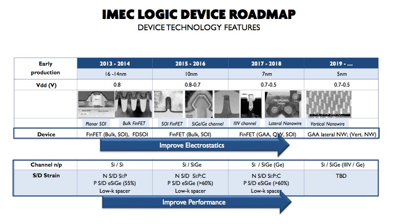
Imec logic device roadmap - Device technology features. (Imec/ITF Korea 2015). Here you can see that at 5 nm there is an option for III/V channel material and possibly vertical Nanowire integration. Next time we will get updated from Imec will be at SEMICON West where An Steegen will give a presentation (http://www.semiconwest.org/node/13826)
Then lets´have a look on CEA/ Leti - also a European R&D organization. CEA/Leti together with ST Micro are steaming down a slightly different path than Imec focusing instead on SOI and FD-SOI technology and 3D stacked CMOS. Here a success has already been seen Globalfoundries Fab1 is putting up and running 20 nm FD-SOI technology. Samsung has signed a deal with ST Micro for the same - yet another european success story in Advanced CMOS scaling.
So to come to the point - when do you hear about scaled advance Logic device data on 300 mm coming out of CNSE or Sematech in New York the last years? How much has been invested there compared to the itty bitty 300 mm R&D Fabs in Europe? I may have missed certain findings but I am sure there is not much out there from Albany. OK they have a different task maybe, more focus on production and so on but at the end of the day much of the cool stuff still comes out of European R&D Pilot fabs.

Why is it so? Here are my thoughts and I would be interested in yours so please do not hesitate to use the comment field or drop me a private e-mail (jonas.sundqvist@baldengineering.com)
1) The management in Europe are Researchers and Innovators themselves - look at Imec, all the top level management, including the CEO Luc Van den Hove, are University Professors. They are not just holding the title here, they are leading research and students. I once took part in a series of workshops between Fraunhofer, TU Dresden and Imec top level managment and when it came to schedule the next meeting we had to adjust time in accordance to upcoming student exams in Germany and Belgium - Would this happen in The US at that level?
Regarding the top management, I assume you have a similar situation at CEA/Leti and not to mention Fraunhofer - you can´t be taken serious in Fraunhofer unless your title starts with Herr Prof. Dr. Dr. In america they are all called Bill or George! Anything but Sue!
Regarding the top management, I assume you have a similar situation at CEA/Leti and not to mention Fraunhofer - you can´t be taken serious in Fraunhofer unless your title starts with Herr Prof. Dr. Dr. In america they are all called Bill or George! Anything but Sue!
2) The track record. Imec and CEA/Leti has a long track record at their current locations and has not been forced to move - look at Sematech they had to move from warm Texas to Up State New York. People must have died the first weeks of winter out of frost bite. You just can´t move top notch researcher - not even in the US.
3) Cross national Collaboration - in Europe all Universities are forced to collaborate with each other to become funded by the EU and in many cases also by the national funding organizations and it does´t matter if you fiddle around with coupons or shuffle 300 mm wafers - the same rules and incentives for everybody. In The US I have a sense that only the 4/6 inch wafer based National Labs and University Cleanrooms have to do this and that they are then financed partly by DARPA and Dr. Polla at IARPA - so the cool stuff is done on small wafers and then the industry steps in and scale it up. Please do correct me if I have the wrong picture here.
So a great success in European Semiconductor R&D that ends when it is time for production - then the Value Chain is sort of half broken - who cares we get to do the cool stuff and the Americans and Asians to shuffle the wafers in Mega Fabs and each wafer will travel at high speed and make multiple passes through an ASML super advanced Lithography tool.


ASML Lithography tool Installed at Imec 300 mm line in Leuven, Belgium (www.imec.be)
They have helped me loads to get me out of the predicament! Counseled to all! Assess your principles and values
ReplyDelete