


%20(1).png)
Researchers from The National Center for Nanoscience and Technology and Hubei University People's Republic of China has presented result on synthesis of large-area (4 × 2 cm2) high quality monolayer h-BN with an ultraclean and unbroken surface on copper foil by using LPCVD.
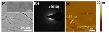
Monolayer h-BN, SAED diffraction and h-BN on SiO2/Si substrate (Source : http://nanotechweb.org/cws/article/lab/61589).
Ultraclean and large-area monolayer hexagonal boron nitride on Cu foil using chemical vapor deposition
Yao Wen, Xunzhong Shang, Ji Dong, Kai Xu, Jun He and Chao Jiang
2015 Nanotechnology 26 275601. doi:10.1088/0957-4484/26/27/275601
Atomically thin hexagonal boron nitride (h-BN) has been demonstrated to be an excellent dielectric layer as well as an ideal van der Waals epitaxial substrate for fabrication of two-dimensional (2D) atomic layers and their vertical heterostructures. Although many groups have obtained large-scale monolayer h-BN through low pressure chemical vapor deposition (LPCVD), it is still a challenge to grow clean monolayers without the reduction of domain size. Here we report the synthesis of large-area (4 × 2 cm2) high quality monolayer h-BN with an ultraclean and unbroken surface on copper foil by using LPCVD. A detailed investigation of the key factors affecting growth and transfer of the monolayer was carried out in order to eliminate the adverse effects of impurity particles. Furthermore, an optimized transfer approach allowed the nondestructive and clean transfer of the monolayer from copper foil onto an arbitrary substrate, including a flexible substrate, under mild conditions. Atomic force microscopy indicated that the root-mean-square (RMS) roughness of the monolayer h-BN on SiO2 was less than 0.269 nm for areas with fewer wrinkles. Selective area electron diffraction analysis of the h-BN revealed a pattern of hexagonal diffraction spots, which unambiguously demonstrated its highly crystalline character. Our work paves the way toward the use of ultraclean and large-area monolayer h-BN as the dielectric layer in the fabrication of high performance electronic and optoelectronic devices for novel 2D atomic layer materials.
No comments:
Post a Comment