Thursday, August 22, 2019

Micron has started volume production of 10 nm-class DRAM (1z nm)

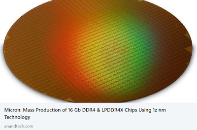
Micron announced on Thursday that it had started volume production of memory chips using its 3rd Generation 10 nm-class fabrication technology (also known as 1Z nm). The first DRAMs to be made using Micron’s 1Z nm process are 16 Gb monolithic DDR4 and LPDDR4X devices. 
The company claims that its 16 Gb DDR4 device consumes 40% less power than two 8 Gb DDR4 DRAMs (presumably at the same clocks). Meanwhile, Micron’s 16 Gb LPDDR4X ICs will bring an up to 10% power saving. One of the first products to use the company’s 16 Gb DDR4 devices will be high-capacity (e.g., 32 GB and higher) memory modules for desktops, notebooks, and workstations.
Source: Anandtech LINK
----------
By Abhishekkumar Thakur

Thursday, August 15, 2019

ALD at V2019 in Dresden October 9th to 10th with Keynote by Dr. Suntola, Millenium Technology Prize winner of 2018

We are very happy to announce the almost complete program for the ALD Workshop at V2019 in Dresden, October 9th to 10th organized by EFDS:
  • Keynote Lecture to Atomic Layer Deposition by Dr. Tuomo Suntola, Millenium Technology Prize 2018
  • Presentations to “Atomic Layer Deposition” Program (Link) 
  • Workshop 5: October 9 – October 10, 2019Industrial Exhibition for Surface Technologies and adjacent Branches : Medical, Optics, Energy and ALD
  • Industrial Evening & V-Dinner
  • Information to Industrial International Funding
Downloads●  Profile of V2019 [PDF]
●  Time Schedule of V2019 [PDF]
●  Industrial Exhibition for Exhibitors [PDF]
●  Program to Atomic Layer Deposition (engl. Language) [PDF]
●  List of Exhibitors (Link)
●  Information for students and junior employees [PDF]
●  Information for job advertisements [PDF]

Lecutues | 2019.10.09 - FREE FOR ALL - No registration fee required

Lecture, part I


"45 years of ALD"
Prof. Tuomo Suntola, Picosun Oy, Espoo, Finland - Millenium Technology Prize 2018Abstract [PDF]
© Picture: By courtesy of Technology Academy Finland.
Lecture, part II
"Current and Emerging ALD Processes, Precursors and Applications in High Volume Production"
Jonas Sundqvist, Fraunhofer-Institut für Keramische Technologien und Systeme IKTS, Dresden, Germany
Abstract [PDF]
Presenations | 2019.09.10 & 2019.10.10

"Advances in quantitative characterization of thin films with help of AFM-based methods"
Malgorzata Kopycinska-Müller, Fraunhofer-Institut für Keramische Technologien und Systeme IKTS, Dresden, Germany
Abstract [PDF]

"In situ metrology for Atomic Layer Deposition processes"
Martin Knaut, Technische Universität Dresden, IHM, Dresden, Germany
Abstract [PDF]
 
"Conformality in Atomic Layer Deposition"
Véronique Cremers, Plasma Electronic GmbH, Neuenburg, Germany
Abstract [PDF]

"Oxides for Electronics"
Mari Napari, Department of Materials Science and Metallurgy, University of Cambridge, Cambridge, UK
Abstract [PDF]
 
"Atomic Layer Deposition of Indium Nitride using Hexacoordinated In–N Bonded Precursors and NH3 Plasma"
Nathan O´Brian, Linköping University, Linköping, Sweden
Abstract [PDF]
 
"Multi-layer Stacked ALD Coating for Hermetic Encapsulation of Implantable Biomedical Microdevices"
Christoph Hossbach, Picosun group, Espoo, Finnland
Abstract [PDF]
 
"Fast plasma ALD employing de Laval Nozzles for high velocity precursor injection"
Abhishekkumar Thakur, Plasway-Technologies GmbH, Dresden, Germany
Abstract [PDF]

More to follow...

Available: VPHA poster at AVS ALD 2019

[VHPA: aldhistory.blogspot.com] The VPHA poster on the ALD doctoral thesis list was updated, as planned, for the AVS 19th International Conference on Atomic Layer Deposition (ALD 2019) featuring the 6th International Atomic Layer Etching Workshop (ALE 2019), https://ald2019.avs.org/. Figure 1 of the poster below. The poster will be included in the AVS collections, and it is currently available via the http://vph-ald.com website.


  • Link to poster: here 
  • Link to abstract: here
  • Link to supplementary information - with full author list: here
The doctoral thesis collection is still certainly missing entries. Suggestions for additions are welcome. Please preferably provide the information via the Google Sheets file, which all can edit: VPHA-thesis-to-be-added.


*********************
Virtual Project on the History of ALD (VPHA) - in atmosphere of Openness, Respect, and Trust

Tuesday, August 13, 2019

ALDFun Workshop at TU Delft (NL) are now online

The presentations form the ALDFundamentals workshop organized at TU-Delft (NL) as videos of speaker and Powerpoint are now available online.

ALDFundamentals: Presentations LINK


Monday, August 12, 2019

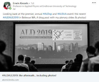
Review of AVS ALD2019 by Prof. Kessels

Please finde here a review of AVS ALD2019 / ALE 2019 by Prof. Kessels, whom recieved the ALD Innovator Award and gave a presentation at the plenary session on Monday morning.

Report: Atomic Limits LINK
Presentation download: Atomic Scale Processing: from Understanding to Innovation LINK


BALD Engineering ALD News blog see doubled visitor traffic last 18 months


The overall monthly visitors to the News Blog doubled in 2018 from about 10,000 to about 20,000. Growth was seen in both the main blog section for ALD Technology news and the ALD Financial News.


The recent trend is increased traffic from India and China. India and China used to contribute to less than 10% of the visitor traffic, but recently they account for more than 25%. The typical monthly geographical origin of the visitors are:
  • 25% USA
  • 25% India and China
  • 25% Germany, France, Russia, Japan, Israel, Finland, and South Korea
  • 25% Rest of the world
Please contact Jonas Sundqvist (jonas.sundqvist@baldengineering.com) for :
  • Banner sponsoring
  • Promotional blogs & press releases
  • Announcing ALD events (conferences, workshops, exhibitions)
  • Become a guest blogger

Friday, August 9, 2019

Lam Research Adds Global Wafer Stress Management Solutions to Portfolio to 3D NAND Scaling

FREMONT, Calif., Aug. 07, 2019 (GLOBE NEWSWIRE) — Lam Research Corp. (Nasdaq: LRCX) today announced new solutions to help customers increase chip memory density, which is needed for applications such as artificial intelligence and machine learning. With the introduction of VECTOR® DT for backside deposition and EOS® GS wet etch for film removal on backside and bevel, Lam continues the expansion of its stress management product portfolio.

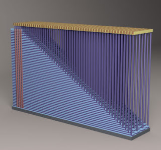
While high aspect ratio deposition and etching are key enablers for 3D NAND scaling, the combination of increasing the number of layers while controlling wafer bow due to cumulative stress in the film stack has become a major challenge. Such stress-induced wafer distortion has a significant impact on wafer yield due to degraded lithography depth-of-focus, overlay performance, and structural distortion. To improve overall yield, wafer-, die-, and feature-level stresses need to be carefully managed at various steps throughout the entire manufacturing process flow, at times potentially resulting in the preclusion of otherwise performance-enhancing process steps due to their stress characteristics.

Designed to provide a cost-effective solution for controlling wafer bow in 3D NAND manufacturing, the VECTOR DT system is the newest addition to Lam’s plasma-enhanced chemical vapor deposition (PECVD) product family. VECTOR DT provides a single-step solution for wafer shape management by depositing a tunable counter-stress film on the back of the wafer without contacting the front side, thereby enabling improved lithography results, reduced bow-induced failures, and integration of high performance but highly stressed films. With strong customer adoption since its debut, the VECTOR DT installed base continues to grow as customers are transitioning to more than 96 layers.

In addition to depositing a counter stress film, Lam provides the flexibility to remove backside films, allowing customers to adjust wafer stress during the 3D NAND manufacturing flow. Lam’s EOS GS wet etch product complements the VECTOR DT by simultaneously removing backside and bevel films with industry-leading wet etch uniformity, while fully protecting the wafer front side. As part of a comprehensive wafer bow management solution, Lam’s EOS GS has also been adopted by memory manufacturers worldwide.

“As our customers continue to dramatically increase the number of memory cell layers, the cumulative stress and wafer bow can exceed the limits of a lithography tool. Minimizing stress-induced distortion is critical for achieving the desired yield and enabling the cost-per-bit roadmap,” said Sesha Varadarajan, senior vice president and general manager of the deposition product group at Lam Research. “With the addition of the VECTOR DT and EOS GS systems, we are expanding our stress management solutions portfolio for managing global stress in support of our customers’ vertical scaling roadmap.”
Source: Lam Research LINK

---------------------
By Abhishekkumar Thakur

Thursday, August 8, 2019

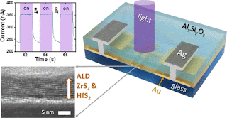
Atomic Layer Deposition of Emerging 2D Semiconductors, HfS2 and ZrS2, for Optoelectronics

Miika Mattinen from Prof. Mikko Ritala's group, University of Helsinki, reports the ALD growth of 2D HfS2 and ZrS2—the potential rivals of the hot favorite 2D semiconductors MoS2 and WSe2. 


Abstract: Semiconducting 2D materials are studied intensively because of their promising performance in diverse applications from electronics to energy storage and catalysis. Recently, HfS2 and ZrS2 have emerged as potential rivals for the commonly studied 2D semiconductors such as MoS2 and WSe2, but their use is hindered by the difficulty of producing continuous films. 

Herein, we report the first atomic layer deposition (ALD) processes for HfS2 and ZrS2 using HfCl4 and ZrCl4 with H2S as the precursors. We demonstrate the deposition of uniform and continuous films on a range of substrates with accurately controlled thicknesses ranging from a few monolayers to tens of nanometers. The use of semiconductor industry-compatible precursors and temperatures (approximately 400 °C) enables facile upscaling of the process. The deposited HfS2 and ZrS2 films are crystalline, smooth, and stoichiometric with oxygen as the main impurity. 


----------------------
By Abhishekkumar Thakur

Tuesday, August 6, 2019

ALD online education course Summer 2019 by Prof. Han-Bo-Ram Lee, of Incheon National University.

Here is an excellent source of ALD online education by Prof. Han-Bo-Ram Lee, of Incheon National University.

ALD Class in English 2019 Summer
1. Review of Fundamentals (https://lnkd.in/fqjD9_N
2. Introduction of ALD (https://lnkd.in/fKdaq46
3. Basic Growth Characteristics of ALD (https://lnkd.in/fAzq9DY
4. ALD Precursors & Reactants (https://lnkd.in/frDVvXA
5. ALD Systems (https://lnkd.in/fyYbzGZ
6. ALD Applications for Si Devices (https://lnkd.in/fCW6cDd
7. Atomic Crafting Beyond ALD (https://lnkd.in/fJZEQEH)

Monday, August 5, 2019

ASM International NV 2019 Q2 Results - Earnings Call

ASM International N.V. (Euronext Amsterdam: ASM) today reports its second quarter 2019 operating results (unaudited) in accordance with IFRS.

• New orders were €373 million. Excluding €103 million related to the patent litigation settlement new orders were €270 million.

• Net sales for the second quarter 2019 were €363 million. Excluding €103 million related to the patent litigation settlement, net sales were €260 million and increased 5% compared to the previous quarter.

• Gross profit margin was 59.0% in Q2 2019 and 42.8% excluding the patent litigation settlement compared to 41.3% in the previous quarter.

• Operating result increased to €150 million. Excluding the patent litigation settlement operating result was stable at €47 million compared to the previous quarter.

• Normalized net earnings, including the patent litigation settlement, for the second quarter 2019 increased by €72 million compared to Q1 2019. Besides the positive impact of the patent litigation settlement net earnings in Q2 were negatively impacted by adverse currency effects and the increase in taxes due to the full utilization of the remaining net operating losses in the Netherlands. Results from investments decreased to €2 million.


ASM INTERNATIONAL N.V. REPORTS SECOND QUARTER 2019 RESULTS

"Logic bookings increased compare to Q1 and were primarily driven by 10 nanometer related demand and early tools for 7nm. Foundry orders decreased so much compared to the record high level in Q1 and primarily reflected its further investments into 5 nm node. Memory orders during the second quarter increased compared to a low level in Q1 mainly driven by DRAM, The increased DRAM bookings during the quarter were largely related to specific customer demands, and in our view not indicative of a broad base recovery in spending in this segment. 
Looking at the bookings by product line, while ALD was again our largest product line, we also experienced healthy demand in for instance LPCVD and Epi business in the quarter. In terms of product lines ALD continues to be a solid driver for our company. 
The long-term outlook remains strong. The current most advanced nodes 10-nanometer in logic and 5-nanometer in foundry have been a major inflection in terms of ALD needs, driven by further miniaturization, new materials, and by new more complex device architecture, that are on the industry's roadmap, the need for additional ALD applications at future nodes will only further increase. This will support continuing healthy growth in these segments of the ALD market over the longer-term. 
Our focus in the memory segments of the ALD market remains the expansion of our swift available market, or so called SAM. We continue to invest in broadening our portfolio of ALD applications for future DRAM and 3D NAND device technology. In 3D NAND for instance as the industry moves to higher stacks of the 96 layers, 128 layers and beyond, the increasing device complexity and high aspect ratio structures will stimulate the needs for a higher number of single wafer ALD applications . We are targeting to increase our SAM and our share of the memory market step-by-step, as customers transition to next generation devices over the next years."

-CEO Charles del Prado

ASM International NV's (ASMIY) CEO Charles del Prado on Q2 2019 Results - Earnings Call Transcript by Seeking Alpha | LINK

Investor presentation Q2 2019 | LINK

Analyts reports:

ASM International: Strong Headwinds We Didn't Hear In Conference Call
Seeking Alpha: ASM International NV (OTCQX:ASMIY) reported 2Q earnings on July 23, 2019. According to financial disclosures, net sales for the second ...

Sunday, July 28, 2019

Strem offer hafnium metal alkylamide ALD precursors for emerging memory applications


Having been extensively studied over three decades for the replacement of silicon dioxide (SiO2) in conventional semiconductor fabrication, ALD Hafnium Oxide (HfO2) among other high-k dielectrics was finally adopted by Samsung in 2004 in high volume manufacturing at the 90 nm DRAM node as the high-k capacitor dielectric. The other DRAM companies followed, and later in 2007 Intel introduced ALD HfO2 at the 45 nm node as high-k gate dielectric. On account of its high dielectric constants (at least four times that of silicon dioxide) a thicker film of hafnium oxide can be used to achieve the same dielectric performance resulting from a thinner silicon dioxide layer without the associated high leakage current or even electron tunneling for ultra-thin dielectrics. High refractory oxides such as those of zirconium and hafnium also find uses in optical applications; as catalysts; and, because of their hardness and thermal stability, as protective coatings.


In recent years, hafnium oxide (as well as doped and oxygen-deficient hafnium oxide) has attracted additional interest as a possible candidate for resistive-switching memories (ReRAM) and CMOS-compatible ferroelectric field effect transistors and memory chips. A great example is Dresden based NaMLab and The Ferroelectric Memory Company (FMC) who are integrating HfO2 based ferroelectric transistor (FeFET) memory. The FeFET is a long-term contender for an ultra-fast, low-power, and non-volatile memory technology. In these devices, the information is stored as a polarization state of the gate dielectric and can be read non-destructively as a shift of the threshold voltage. The advantage of a FeFET memory compared to the Flash memory is its faster access times and much lower power consumption at high data rates.
Moreover, in the framework of a project together with GLOBALFOUNDRIES and Fraunhofer IPMS, a one-transistor (1T) FeFET eNVM was successfully implemented in a 28 nm gate-first super low power (28SLP) CMOS technology platform using only two additional structural masks. Since then, other companies and researchers have followed and the “ferroelectric HfO2 community” have met on an annual basis in Dresden at the NaMLab annual Novel high-k workshop for more than a decade now. The most recent trend is that HfO2 may enter a 2nd time in DRAM manufacturing, this time as a high-k gate oxide for the select transistor.
When grown using chemical vapor deposition (CVD) from β-diketonate precursors, alkoxide precursors, and chloride precursors, a relatively high (typically greater than 300 °C) deposition temperature is required, which results in rough films because of their high crystallinities. ALD based HfO2 films employing both chloride and iodide precursors arefeasible as low as 180 °C, but then typically exhibit high incorporation of chlorine and iodine impurities. As for the CVD processes mentioned above, the high temperatures needed to prevent this contamination result in the formation of highly crystalline films with apparent surface roughness. Etching of the growing oxide surface by the precursors themselves also causes additional surface roughening and non-conformality. The etching might also explain the difficulty in depositing a conformal coating on high-aspect-ratio structures using these halide precursors. 

To address these concerns, Professor Roy G. Gordon and members of his laboratory at Harvard, in the late 1990s and early 2000s, invented metal alkylamide precursors to create thin films of high-k dielectric materials (e.g., HfO2, ZrO2). They also filed patents for their innovation at the US Patent Office in 2000.

The metal alkylamide precursors (e.g., TEMAHf) produce less corrosive byproducts compared with halide precursors (e.g., HfCl4). The byproducts themselves neither etch the adsorbates nor cause additional surface roughness, which in turn affords good conformal coating on high aspect ratio structures. As a liquid precursor, they can be easily vaporized, unlike solid HfCl4, yielding significant growth-per-cycle (GPC) due to high transport efficiency. There is no chlorine contamination in the deposited HfO2 film, which leads to reduced interface charges, improved dielectric properties, and suppressed leakage current. Metal alkylamides also exhibit higher reactivity, which enables lower deposition temperature. In general terms, the hafnium alkylamide precursors are preferred for high aspect ratio applications like DRAM and 3D MIM Capacitors, while for planar logic and FinFET devices hafnium chloride is typically used.

Strem Chemicals, Inc., a leading fine chemicals supplier, headquartered in Newburyport, Massachusetts, USA, boasts a vast variety of metal alkylamide precursors for depositing Hf-based materials in different applications. The table below outlines three Hf-based metal alkylamide precursors from Strem’s catalog.

Please find here one of the well-cited publications on ALD of HfO2 from Prof. Gordon’s Harvard laboratory. This article from 2002 takes advantage of the above three Hf alkylamides and water in deep trench DRAM structures (from Infineon) to study the properties of the deposited oxide films by Hausman et al.

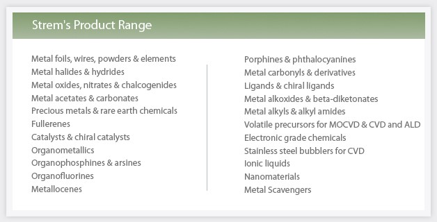
About Strem Chemicals: Strem is an employee-owned specialty chemicals supplier, manufacturing, and marketing high quality specialty chemicals for more than half-a-century. They provide custom synthesis, and FDA inspected current good manufacturing practice (cGMP) services to their clients from academia, industry and government R&D labs. What distinguishes Strem from other chemicals suppliers is their continued commitment to quality. This help Strem deliver precursors with, by and large, 99% metals purity including some metal precursors with even 99.9999% purity. Strem offers over 5,000 specialty products in the area of metals, inorganics, organometallics, and nanomaterials. Strem’s product range includes:

 
 ----------
Promotional blog written and researched by Abhishekkumar Thakur and Jonas Sundqvist, BALD Engineering AB