Wednesday, October 28, 2020
TechInsights Webinar: ALD/ALE Process in Commercially Available Memory Devices
Tuesday, October 6, 2020
Heads up ALD-people! On Thursday the ALD Symposium at PRiME2020 start and it is FOR FREE!
This week, the Virtual PRiME 2020 Joint International Meeting will be held under the auspices of
The Electrochemical Society (ECS), The Electrochemical Society of Japan (ECSJ), and The Korean Electrochemical Society (KECS).
Over 75% of the 3,300+ original abstracts, meant for presentation in Honolulu (Hawaii) this week, are available as digital presentations.
On the online program you can find all info on the presentation files (video, slides, and/or posters).
These can be viewed on-demand in open-access mode, from Oct. 4 – Nov. 9, 2020.
Attendance and participation in PRiME 2020 is FREE and OPEN TO ALL! Only your pre-registration is required.
This includes Symposium G02 that I co-organized: G02 - Atomic Layer Deposition Applications 16.
See the information below for some more general info on our ALD symposium, also on the live sessions on Oct. 7 and 8, Hawaii HST time (!))
Opening remarks presentation. file:///C:/Users/jonas/AppData/Local/Temp/Opening_Welcome-Symp.%20G02_Fred%20Roozeboom_Oct20.pdf
We were sponsored by
Monday, August 24, 2020
TechInsights ALD/ALE Process in Commercially Available Logic Devices
2018 saw the introduction of a new generation of logic products featuring finFET transistors headlined by Intel with their 10 nm generation microprocessor, followed by TSMC and Samsung towards the end of the year with their 7 nm node devices.
This presentation on the Atomic Layer Deposition/Atomic Layer Etching (ALD/ALE) process examines some of the different structures we have seen during the evolution of these logic technologies, in particular the latest 7 nm and 10 nm devices. We also discuss several historical applications of ALD/ALE technology that have been observed through reverse engineering, and we highlight the importance of ALD/ALE process in advanced logic devices. In many cases, the technology could not have advanced without the implementation of ALD/ALE.
Register here: LINK
Friday, May 15, 2020
Holst Centre will organize a series of free webinars about Spatial Atomic Layer Depoisition. Registration will open soon.
Monday, January 20, 2020
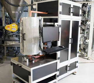
Forge Nano Webinar - Lab Scale ALD on powders with PROMETHEUS
FREE ALD Webinar - Lab Scale ALD on powders with PROMETHEUS
- Join the ALD experts at Forge Nano for a free webinar on Jan. 30th @ 10:00am MST.
- Join us as our experts demonstrate our Lab-Scale ALD tool- PROMETHEUS.
- Get an up-close and personal look at the features and functionality of PROMETHEUS.
PROMETHEUS is a Lab-Scale, Particle ALD research tool like no other. Featuring a simple to use interface, ergonomic and intuitive design, and various reactor sizes and configurations.
Previous Webinar - ALD Basics – ALD on powders (LINK)
Friday, November 9, 2018
Introductory lecture on ALD available as "Panopto" lecture capture, and slides in SlideShare
Thursday, May 24, 2018
NEW! AVS Short Course Webinar on Atomic Layer Etching (ALE)
|
|
|
Atomic Layer Etching (ALE):
June 13,2018
REGISTRATION DEADLINE: June 11, 2018
|
Tuesday, April 10, 2018
AVS Short Course Webinar on Atomic Layer Etching (ALE) June 13,2018
|
Atomic Layer Etching (ALE):
June 13,2018
REGISTRATION DEADLINE: June 11, 2018
|
||||
The AVS Short
Course Webinar focusing on Atomic Layer Etching (ALE) will be held
on Wednesday, June 13, 2018 from 1:00-5:00 p.m (EDT). This webinar will be
taught by Steven M. George, Professor in the Dept. of Chemistry & Biochemistry
and Dept. of Mechanical Engineering, University of Colorado at Boulder. This
AVS Webinar on ALE will provide the training required to understand
plasma-assisted ALE and thermal ALE. The webinar will explain the
process strategies for plasma-assisted ALE and thermal ALE. Important
ALE approaches for many materials including Si, SiO2, Al2O3, TiN and W will be
described that are useful for advanced semiconductor processing.
Who should attend: Scientists, engineers and technicians who
use or plan to use atomic layer etching for atomic scale fabrication.
Date: June 13, 2018
Time: 1:00-5:00 p.m. (EDT)
Cost: $200/person
REGISTRATION
DEADLINE: June 11, 2018
Questions: E-mail heather@avs.org or call
530-896-0477.
|
Thursday, April 5, 2018
FREE webinar: Optimising ALD high-k oxides for novel applications
The webinar will comprise of two talks, with a Q&A session at the end. Register here


Wednesday, April 4, 2018
Thursday, March 1, 2018
Beneq offers online training in Atomic Layer Deposition
Train yourself online on ALD - Introducing Beneq Thin Film Solutions webinar series
As experts of Atomic Layer Deposition and thin film coatings, we get a lot of questions about ALD from our customers and partners as well as students and other people with an interest in nanotechnology. The questions and information requests range from very general questions about the ALD technology and its application possibilities to extremely detailed thin film research problems.
Wednesday, March 21st at 3.00 PM EET
In this webinar, Timo Rantasalmi, Head of Customer Services, will walk you through the available option and upgrades with concrete examples of their use and benefits.
2. Introduction to Beneq Coating Services
Wednesday, April 4th at 3.00 PM EET
In this webinar, Dr. Erik Østreng, Head of Coating Services, will explain the benefits of using Beneq Coating Services, introduce the typical coating service solutions and tell you how to get started.
Beneq Webinar Page for full details LINK
Sunday, January 28, 2018
Atomic Layer Deposition (ALD): Basic Principles, Characterizations, and Applications
Thursday, March 15, 2018, 1:00-5:00 p.m. (EDT)
The AVS Short Course Webinar focusing on on Atomic Layer Deposition (ALD) will be held on Thursday March 15 at 1:00 PM eastern time. This webinar will be taught by AVS Instructor, Robert K. Grubbs. Dr. Grubbs has been working in the field ALD for 20 years and has applied the ALD process to solve myrid technical challenges in the semiconductor industry and in the area of national security (Principal Member of the Technical Staff at Sandia National Laboratories).Registration: LINK
Wednesday, August 30, 2017
Webinar - ALD for 2D materials
- Atomic Layer Deposition for Graphene devices by Dr Daniel Neumaier, AMO GmbH
- Atomic Layer Deposition on and of 2D materials by Dr Harm Knoops, Oxford Instruments
Wednesday, June 14, 2017
Atomic Scale Processing Webinar with Oxford Instruments
Atomic Scale Processing | 15th June, 3:30pm BST
• Atomic scale processing: Atomic Layer Deposition & Etching
Dr Harm Knoops
• Processing of atomic scale materials & devices: Graphene & 2D
materials | Dr Ravi Sundaram
Friday, March 24, 2017
Wednesday, March 8, 2017
Webinar on Atomic Layer Deposition (ALD) Market Analysis
Description
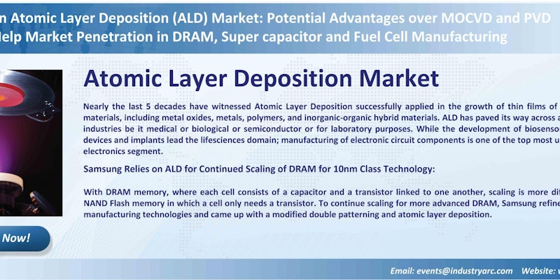
Samsung Relies on ALD for Continued Scaling of DRAM for 10nm Class Technology:
With DRAM memory, where each cell consists of a capacitor and a transistor linked to one another, scaling is more difficult than with NAND Flash memory in which a cell only needs a transistor. To continue scaling for more advanced DRAM, Samsung refined its design and manufacturing technologies and came up with a modified double patterning and atomic layer deposition.The Fuel Cell and ALD Overhaul:
ALD has clearly gained prominence in manufacture of fuel cell. IndustryARC predicts high potential in this field in the coming years. Solid Oxide Fuel Cells are noted a quality contribution to the global ALD market:Durable and high-performance low temperature solid oxide fuel cells
ALD of ultrathin blocking layer for low-temperature solid oxide fuel cell on nanoporous substrate
Supercapacitors Manufacturing: ALD to the Rescue?
With the invent of ALD, energy conversion, producing cost competitive, durable and high performance devices have become increasingly significant and one such application is manufacture of a supercapacitor! Manufacturers, developers and suppliers of supercapacitors have lately gained utmost ascendancy. ALD encapsulated activated carbon electrodes for high voltage stable supercapacitors- continue to trend in the market.Wednesday, November 16, 2016
Oxford Instruments Plasma Technology free webinars
The two most recent webinars:
Growth and Characterisation of 2D Materials Beyond Graphene
Dr Ravi Sundaram, Oxford Instruments & Dr Tim Batten, Renishaw
SiC Via Etching for RF Devices
Oxford Instruments Plasma Technology
Sunday, June 1, 2014
Webinar: Use of ALD for MEMS and NEMS Applications by Oxford Instrument Plasma Technology
Wednesday, July 2, 2014 11:30 AM - 12:30 PM EDT
Presented by Dr. Harm Knoops, Technical Sales Specialist (ALD) at Oxford Instrument Plasma Technology
Monday, February 24, 2014
Webinar Taking Nano to the next level. Speakers from LBNL and Seagate!
This webinar is free of charge, and will run for 1 hour including time for questions and answers at the end. A focus on recent nanoscale etch and atomic layer deposition (ALD) advances from research to
manufacturing applications, from industry leading speakers:
Talk 1: ALD and nanoscale etch processing techniques and results from recent work carried out at Lawrence Berkeley National Laboratory (LBNL), USA
Speaker: Deirdre Olynick, Staff Scientist, LBNL, CA, USA
Talk 2: Data storage, an expanding market application that has benefited from advanced ALD and nanoscale etch techniques
Speaker: Kim Lee, Seagate, CA, USA


%20(1).png)


