Showing posts with label Picosun. Show all posts

Wednesday, March 25, 2020

Picosun reinforces local operations to ensure customer satisfaction during the COVID-19 epidemic

ESPOO, Finland, 23rd March 2020 – Picosun Group’s first priorities are customer satisfaction and health and wellbeing of the Group’s employees and customers. Picosun takes extremely seriously the global threat posed by the COVID-19 novel coronavirus epidemic and follows the rules set by governments and WHO. As the epidemic restricts global traveling, the importance of local offices and subsidiaries close to the customers is of utmost importance.


The last years have been the time of rapid growth and expansion for Picosun. Strong emphasis has been put on new recruitments especially on the service and support sector. Trained and qualified staff of service engineers are on call at the Group’s US locations in Texas, Arizona, and California and Asian locations in Japan, China, Taiwan, and Singapore. Dedicated sales and support personnel in Germany and France are available for the Group’s European customers. Local process support is also available on each continent.

At Picosun’s Finnish headquarters and local offices employees are encouraged to remote work from home whenever possible. Meetings are arranged virtually via video links and online platforms and inviting external visitors to the company’s premises is minimized to bare necessities. Cleaning of the premises and other hygiene measures have been intensified. All recruitment interviews are conducted remotely.

Despite of the challenging times, Picosun’s customer projects and deliveries continue. Process support and applications consultancy is always available from our Ph.D. level experts, and our Helpdesk serves 24/7 at support@picosun.com. Delivered PICOSUN® ALD system installations and commissioning, as well as customer support on-site, are taken care of by local Picosun offices with their trained and experienced staff.

“All of us here at Picosun wish good health and safety to everybody in this difficult and unexpected situation. In times like this, collaboration is the key to success and speedy recovery. Our business continues and we will put all our effort in sustaining the high level of quality that is the trademark of Picosun. We will further intensify our efforts to bring the benefits of ALD to medical industry. ALD is the very technology that enables our modern, mobile, data-driven and interconnected global society. Now is the time when this society can truly work together for better future,” says Jussi Rautee, CEO of the Picosun Group.

For more information regarding your projects or deliveries, please contact your respective Picosun sales or support contact person. For quotations for our ALD equipment and solutions, or process demo, please contact sales@picosun.com or coating@picosun.com, respectively.

As several expos and conferences the Group is sponsoring or exhibiting at have been postponed, please see the new dates in our event calendar on our website. Picosun is looking forward to meeting you all again later this year in good health and spirits!

Thursday, February 27, 2020

Picosun delivers multiple production ALD systems to Asia for solid state lighting device manufacturing

ESPOO, Finland, 26th February 2020 (LINK) – Picosun Group, Finland-based, global provider of advanced Atomic Layer Deposition (ALD) thin film coating solutions, has been chosen by a major Asian customer to deliver significant ALD production capacity for manufacturing of solid state lighting devices. 

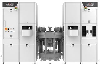
The PICOSUN® P-300BV ALD system is specially designed for production of LEDs, discrete devices, and MEMS devices such as print heads, sensors, and microphones.
 
Solid state illumination technologies are the future of lighting. Running on much lower power than other lighting devices and lasting much longer, they save both resources and environment. As small, compact and light-weight they are also simple to use in remote locations such as rural areas in developing countries, thus providing safe and easily powered lighting for example for children to study or health care stations to operate.

Picosun wants to introduce ALD to applications where it can improve both people’s quality of life and the state of the environment. Indeed, ALD is an ideal technology to enable various sustainable solutions, not only in lighting but in various other industries. In many cases, replacing thick, lower quality coatings with ultra-thin but superior quality ALD films leads to both material and energy savings and longer end product lifetime. Picosun’s equipment design, refined to top-notch performance through decades of cumulative experience in the field, ensures that no matter what industry, an optimal coating solution can always be found from the company’s portfolio.

“ALD films enhance the performance and lengthen the lifetime of solid state lighting devices. Our PICOSUN® P-300BV ALD system is specifically designed for these applications. It combines fast batch production capacity with vacuum loading for the highest ALD film quality and purity. We are happy to be chosen as the ALD technology provider for our esteemed customer. A facility of multiple P-300BV ALD tools that shall be installed in their premises will significantly strengthen our position in this market. For the end users, our ALD solutions enable flexible, power-saving and environmentally friendly lighting solutions with superb brightness and long life,” says Mr. Edwin Wu, CEO of Picosun Asia Pte. Ltd.

Thursday, January 30, 2020

Picosun’s ALD technology helps to fight climate change

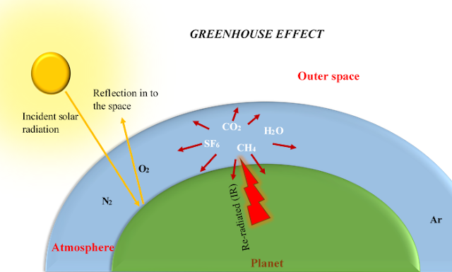
ESPOO, Finland, 30th January 2020 – Picosun’s Atomic Layer Deposition (ALD) thin film barrier coating technology offers a solution for eliminating the use of hazardous process gases, sulphur hexafluoride (SF6) and nitrogen trifluoride (NF3).

In the current Chemical Vapor Deposition (CVD) coating methods, relatively thick films need to be grown to obtain the desired level of performance to reach the required specifications in e.g. moisture barrier, corrosion protection, passivation or insulation applications. Due to the fast film build-up on the walls of the coating equipment, the deposition chamber has to be cleaned of film residues at regular intervals. This is typically done by a chamber cleaning process with SF6 or NF3 plasma.


SF6 is the strongest greenhouse gas ever known, with global warming potential of 22600 times that of CO2 (for NF3, the coefficient is 17200) and it stays in the atmosphere for at least 1000 years (*). SF6 emissions in the EU in 2017 alone had greenhouse gas effect equalling that of 1,4 million cars (**). Hence, usage of these gases is subject to constant scrutiny and increased regulation.

By switching to Picosun’s ALD nanolaminate barrier technology it is possible to obtain unmatched barrier performance with extremely thin, pinhole-free films. This also eliminates the need to clean the deposition equipment after every few process runs. In typical production use, Picosun’s ALD reaction chamber is cleaned only once per 3 – 6 months, and simple mechanical bead blasting instead of fluorine-based plasma treatment is enough.

“We at Picosun want to employ our ALD technology for sustainable future. Fighting the climate change by all possible means requires collaboration between the innovative industries and solution providers. By replacing thick coatings, manufactured with environmentally compromising, energy- and resource-intensive methods, with our ultra-thin ALD film stacks, significant material and cost savings are obtained and hazardous gases are not needed in equipment cleaning,” summarizes Mr. Juhana Kostamo, deputy CEO of Picosun Group.

Picosun provides the most advanced AGILE ALD® (Atomic Layer Deposition) thin film coating solutions for global industries. Picosun’s ALD solutions enable technological leap into the future, with turn-key production processes and unmatched, pioneering expertise in the field – dating back to the invention of the technology itself. Today, PICOSUN® ALD equipment are in daily manufacturing use in numerous leading industries around the world. Picosun is based in Finland, with subsidiaries in Germany, North America, Singapore, Taiwan, China and Japan, offices in India and France, and a world-wide sales and support network. Visit www.picosun.com.

(*) J-C. Cigal et.al.: “On-site fluorine chamber cleaning for semiconductor thin-film processes: Shorter cycle times, lower greenhouse gas emissions, and lower power requirements”, DOI: 10.1109/ASMC.2016.7491126

(**) P. Widger et.al.: “Evaluation of SF6 leakage from gas insulated equipment on electricity networks in Great Britain”, DOI: 10.3390/en11082037

Friday, January 24, 2020

Program release - EFDS ALD for Industry 2020 in Freiburg, Germany (March 31-April 1)

A topical workshop with a focus on industrialization and commercialization of ALD for current and emerging markets

Atomic Layer Deposition (ALD) is used to deposit ultraconformal thin films with sub-nm film thickness control. The method is unique in the sense that it employs sequential self-limiting surface reactions for growth in the monolayer thickness regime. Today, ALD is a critical technology in leading-edge semiconductor technology, and the field of application in other industries is increasing rapidly. According to the market estimates, the equipment market alone is currently at an annual revenue of US$ 1.8-1.9 billion (2018), and it is expected to double in the next 4-5 years. In a European context, ALD was invented independently twice in Europe (Russia & Finland), and since the last 15 years, Germany has grown to become one of the strongest European markets for ALD in R&D, chemicals, equipment, and end-users.
Keynote: Prof. Henrik Pedersen, Linköping University
Tutorials by : Bochum University, Lund University, Uppsala University, Oxford Instruments, TECHCET / Fraunhofer IKTS 
Presentations by: Air Liquide, BASF, CEA Leti, Encapsulix, Picosun, Veeco, Sentech, Beneq, Fraunhofer IPMS-CNT, Positive Coating, ATLANT 3D Nanosystems, Fraunhofer FMD 
This year we will organize the 4th Workshop „ALD For Industry“ in South Germany (Freiburg), much closer to the other ALD hubs in continental Europe in France, The Netherlands, Belgium, Italy, and Switzerland. ALD for Industry provides the opportunity to get in contact with industrial and academic partners to learn more about the fundamentals of ALD technology and to get informed about recent progress in the field. The Event will focus on the current markets for ALD and addresses the applications in the Semiconductor industry, MEMS & Sensors, Battery Technology, Medical, Display, Lightning, Barriers, and Photovoltaics.
Program and Information: LINK

ALD Industrial Exhibition (more in the pipeline):


Russian researchers obtain atomically thin molybdenum disulfide (2D) films on large-area substrates by ALD

[Press release: LINK] Researchers from the Moscow Institute of Physics and Technology have managed to grow atomically thin films of molybdenum disulfide spanning up to several tens of square centimeters. It was demonstrated that the material’s structure can be modified by varying the synthesis temperature. The films, which are of interest to electronics and optoelectronics, were obtained at 900-1,000 degrees Celsius. The findings were published in the journal ACS Applied Nano Materials.


An atomic layer deposition reactor from Picosun used for obtaining ultrathin molybdenum oxide films, which were subsequently sulfurized to 2D molybdenum disulfide. Image courtesy of the Atomic Layer Deposition Lab, MIPT

Two-dimensional materials are attracting considerable interest due to their unique properties stemming from their structure and quantum mechanical restrictions. The family of 2D materials includes metals, semimetals, semiconductors, and insulators. Graphene, which is perhaps the most famous 2D material, is a monolayer of carbon atoms. It has the highest charge-carrier mobility recorded to date. However, graphene has no band gap under standard conditions, and that limits its applications.


Thursday, January 2, 2020

Picosun’s ALD technology enables 3D silicon-integrated microcapacitors with unprecedented performance

ESPOO, Finland, 2nd January 2020 (LINK) – Picosun Group, global provider of leading AGILE ALD® (Atomic Layer Deposition) thin film coating solutions, reports record performance of silicon-integrated, three-dimensional deep trench microcapacitors manufactured using its ALD technology.

Increasing efficiency and performance demands of portable and wearable electronics, along with their shrinking size in accordance with the Moore’s law, set new challenges to the power management of these devices as well. A solution is further integration of the devices’ key components into so-called SiP (systems-in-package) or SoC (systems-on-chip) architectures, where everything, including the energy storage such as batteries or capacitors, is packed close to each other into one compact, microscale-miniaturized assembly. This calls for novel techniques to increase the performance and shrink the size of the energy storage unit as well. Three-dimensional, high aspect ratio and large surface area deep trench microcapacitors where ultra-thin, alternating layers of conducting and insulating materials form the energy storing structure, provide a potential solution.


Figures above: Main technological steps of 3D microcapacitor fabrication. 1: patterning of a square lattice of holes on the silicon surface; 2: high aspect ratio trenching of silicon by electrochemical micromachining (ECM); 3: atomic layer deposition (ALD) of conformal metal-insulator-metal (MIM) stack; 4: aluminium deposition and contact patterning (*).

Picosun’s ALD technology has now realized unprecedented performance of these 3D microcapacitors. PICOSUN® ALD equipment were used to deposit film stacks of conductive TiN and insulating dielectric Al2O3 and HfAlO3 layers into high aspect ratio (up to 100) trenches etched into silicon. Up to 1 µF/mm2 areal capacitance was obtained, which is the new record for this capacitor type. Also power and energy densities, 566 W/cm2 and 1.7 µWh/cm2, were excellent and surpassing the values achieved with the most of the other capacitor technologies. The ALD microcapacitors showed also outstanding voltage and temperature stability, up to 16 V and 100 oC, over 100 hours continuous operation (*).


Figures above: b) SEM cross-section of an array of cylindrical trenches with a pitch of 4 μm, diameter of 2 μm and aspect ratio of 100, conformally coated with an ALD stack consisting of 40 nm of TiN, 40 nm of Al2O3, and 40 nm of TiN. Insets show a detail of the MIM stack at the top and bottom of a single trench; d) high-resolution TEM image of an MIM stack consisting of 40 nm of TiN, 40 nm of Al2O3, and 40 nm of TiN taken at the bottom of ALD-coated trenches with aspect ratio of 100; e) TEM-EDX elemental maps of Ti (yellow), N 14 (cyan), Al (red), and O (green) of the MIM stack in (d) (*).

These excellent performance indicators pave the way to industrial applications of this capacitor technology. This is further facilitated by ALD’s mature position in modern semiconductor industries, where the technology is already integrated into practically all advanced microchip component manufacturing lines.

“We exploited the room available on the bottom of silicon wafers, of which only a few micrometers of silicon are used for electronic components in integrated circuits, to fabricate silicon-integrated 3D microcapacitors with unprecedented areal capacitance. The electrochemical micromachining technology, developed at the University of Pisa over the past decade, enabled etching of high density trenches with aspect ratios up to 100 in silicon, a value otherwise not achievable with deep reactive ion etching. This posed the basis for increasing the areal capacitance of our 3D microcapacitors upon conformal coating with an ALD metal-insulator-metal stack,” says Prof. Giuseppe Barillaro, group leader at the Information Engineering Department of the University of Pisa, Italy.

“The suberb results achieved with our 3D silicon-integrated microcapacitors show again how imperative ALD technology is to modern microelectronics. We are happy that we can offer our unmatched expertise and decades of cumulative know-how in the field to develop novel solutions for the challenges the industry is facing, when the requirements for system performance and integration level increase inversely to the system size. The environmental aspect is also obvious, when smaller, more compact devices manufactured in the same line mean also smaller consumption of materials and energy,” says Juhana Kostamo, deputy CEO of Picosun Group.
(*) “Three-dimensional silicon-integrated capacitor with unprecedented areal capacitance for on-chip energy storage”, Lucanos M. Strambinib,1, Alessandro Paghia,1, Stefano Mariania, Anjali Soodc, Jesse Kalliomäkic, Päivi Järvinenc, Fabrizio Toiad, Mario Scuratid, Marco Morellid, Alessio Lampertie, Giuseppe Barillaroa,b,, accepted for publication in Nano Energy, https://doi.org/10.1016/j.nanoen.2019.104281.
a Dipartimento di Ingegneria dell’Informazione, Università di Pisa, via G. Caruso 16, 57122, Pisa, Italy
b Istituto di Elettronica e di Ingegneria dell’Informazione e delle Telecomunicazioni, Consiglio nazionale delle Ricerche, via G. Caruso 16, 57122, Pisa, Italy
c Picosun Oy, Tietotie 3, Espoo, FI-02150, Finland
d ST Microelectronics, via Olivetti 1, Agrate Brianza, Italy
e IMM-CNR, Unit of Agrate Brianza, Via C. Olivetti 2, 20864, Agrate Brianza, MB, Italy
(Funding from the ECSEL Joint Undertaking through the R2POWER300 project, grant no. 653933)

Wednesday, December 4, 2019

High-performance lithium-ion battery materials with Picosun ALD

ESPOO, Finland, 3rd December 2019 – Picosun Group, the provider of AGILE ALD® (Atomic Layer Deposition) thin film coating technology for global industries, reports excellent results achieved with ALD in the manufacturing of lithium ionthin film battery materials.

Solid-state Li-ion thin film batteries (SSLIBs) are small, compact and may have flexible construction. They don’t contain any aggressive liquid substances, so they are safe to use. Furthermore, SSLIBs possess excellent energy storage capacity, which is why they are regarded as ideal power sources for electric cars, laptops, tablets and smartphones, wireless sensors, implantable and wearable medical devices, and harvesting devices for renewable energy sources. The impact of Li-ion battery technology on our modern society, permeated by portable electronics, wireless data transfer and mobile communications, is so huge that it earned its developers, Dr. John B. Goodenough, Dr. M. Stanley Whittingham, and Dr. Akira Yoshino, the Nobel chemistry prize this year.

As the performance requirements of these devices increase, functional characteristics of their power sources should be improved as well. Transition from planar, 2D battery geometry to corrugated 3D one with much higher active surface area for energy storage could augment the energy and power density of SSLIB. However, finding a suitable method for depositing the functional material layers on the complex microscale structures of the 3D batteries poses another challenge.


Diagram of a conventional 2D all-solid-state thin-film Li-ion battery structure (a), its SEM section view (b), and advantages of the 3D battery structure. Image source: Yue et. al., Fabrication of Si-based three-dimensional microbatteries: A review, in Frontiers of Mechanical Engineering 2017 (doi: 10.1007/s11465-017-0462-x).

Picosun’s ALD technology has now been successfully used to fabricate high-quality, high-performance thin film NiO anodes for SSLIBs. Compared to graphite, which is widely used to produce anodes of lithium-ion batteries, deposited NiO films had more than twice as large capacity and more than three times as high density (*). The surpassing characteristics of NiO potentially allow improvement of the energy density of SSLIBs.

In addition to high quality and performance of the ALD NiO anodes, ALD’s unmatched capability to produce conformal and uniform coatings with excellent purity and repeatability inside challenging microscale architectures such as high aspect ratio trenches makes it an ideal method for 3D SSLIB materials manufacturing. Also, the ALD processes for several other anode materials such as SnO2, CoO, and MnO are well-known and thoroughly studied.

“We are very pleased with the PICOSUN® ALD system at our facilities, and all the support and consultancy we have received from Picosun over the years. With our ALD system we have been able to deposit dense, uniform ALD NiO films with low roughness and very high capacity. The excellent qualities of these films allowed us to develop high-performance anodes for SSLIBs,” says Picosun customer, Dr. Maxim Maximov from Peter the Great St.Petersburg Polytechnic University (SPbPU), Russia.

“Battery applications are yet one example of ALD’s flexibility as a method, and how new industries discover the possibilities of ALD day by day. Deep trenches with aspect ratios exceeding 1:2500 have been successfully coated with our ALD tools equipped with our patented Picoflow™ feature, which further advocates the use of our technology in 3D solid state Li-ion battery manufacturing. We are happy that our ALD solutions can be potentially utilized in future’s energy storage solutions in conjunction with clean energy production, and to power more compact healthcare devices, to improve people’s quality of life,” states Dr. Jani Kivioja, CTO of Picosun Group.

Picosun provides the most advanced ALD thin film coating technology to enable the industrial leap into the future, with turn-key production solutions and unmatched expertise in the field. Today, PICOSUN® ALD equipment are in daily manufacturing use in numerous major industries around the world. Picosun is based in Finland, with subsidiaries in Germany, North America, Singapore, Taiwan, China and Japan, offices in India and France, and a world-wide sales and support network. Visit www.picosun.com.

(*) Yury Koshtyal et. al., Atomic Layer Deposition of NiO to Produce Active Material for Thin-Film Lithium-Ion Batteries, Coatings 2019, 9, 301; doi:10.3390/coatings9050301. Open access: https://www.mdpi.com/2079-6412/9/5/301

For more information about the application of ALD in Li-ion batteries, please visit Dr. Maxim Maximov’s profile at https://www.researchgate.net/profile/Maxim_Yu_Maximov.

Monday, November 4, 2019

Picosun expands selection of biocompatible ALD materials for medical applications

ESPOO, Finland, 4th November 2019 – Picosun Group, the leading supplier of AGILE ALD® (Atomic Layer Deposition) thin film coating solutions for global industries, expands its selection of biocompatible ALD materials to be used in medical applications.

Picosun’s TiO2 and Al2O3 processes are already used in production of surgical implants and in drug particlecoating for controlled drug delivery. Now, also HfO2, SiO2, ZrO2, Nb2O5, Ta2O5, AlN and TiN ALD films manufactured by Picosun have been tested and validated by an independent third party to be non-cytotoxic and safe to human tissues in e.g. implant applications (*).

This wide variety of materials gives great flexibility in designing novel ALD solutions for a plethora of healthcare uses, when the materials can be used either as such, or combined into nanolaminates or doped films with unique, application-wise tailorable physico-chemical properties (**). 


Microimplant electronics protected by Picosun’s ALD HfO2. No changes after soaking in 87 oC PBS for over 3 months which correlates to over 10 years in human body. T0 = starting point of the test. Reference: InForMed project, image source CEA-Leti.
 
ALD, with its innate ability to create ultra-thin material layers with the highest conformality, uniformity, and structural quality, has enormous potential to solve various key issues in medical applications where implantable devices are involved. Orthopaedic implants, pacemakers, implantable hearing or eyesight aids, microimplants for sensing, monitoring and analysis applications, and brain or heart probes for therapeutic or diagnostic uses all contain parts that are sensitive to the corrosive environment of the human body. Protective encapsulation of these devices is thus needed to ensure their correct operation, long enough operational lifetime, and also to protect the body from the possible rejection reaction or contaminant leakage from the devices’ corroding parts. Various polymer layers have typically been used as encapsulants, but their downside is their thickness and robustness which unnecessarily increases the mass and dimensions of the implant.  

 
TEM micrographs of Picosun’s ALD nanolaminate and oxide encapsulants after one month soaking tests in 87 oC PBS. No corrosion observed.
 
Compared to polymer encapsulation, ALD offers a truly elegant, sophisticated solution to implant manufacturers. Practically massless and invisible, but still dense, flexible, pinhole- and crack-free ALD thin films cover reliably even the smallest microscale surface features of the coated object, they can be applied at moderate temperatures, and – as now analysed in medical industry’s standard tests – several ALD materials are intrinsically biocompatible. As ALD is a mature, key enabling technology in semiconductor and microelectronics manufacturing for decades already, the processes and practises for industrial introduction and ramp-up exist, and can be readily applied to new fields as well.

”Healthcare sector is one of our key strategic directions. Our patented know-how of ALD-based biocompatible protective encapsulation for implantable medical devices has already raised significant interest amongst industry leading companies. We are pleased that we have now even wider portfolio of materials and solutions that we can provide to these companies. Not only can our ALD technology solve several challenges these industries are currently facing, but also enable completely new components and devices to realize future’s healthcare inventions,” states Dr. Jani Kivioja, CTO of Picosun Group.
 
(*) FICAM – The Faculty of Medicine and Health Technology, University of Tampere, Finland: Cytotoxicity tests with cell culture medium according to the ISO 10993-5 standard, and 3 weeks soaking tests in PBS (phosphate-buffered saline) at 87 oC.

Sunday, September 22, 2019

Picosun Regional Sales and Service Manager, Europe – Dresden, Germany

Picosun is now searching for a Regional Sales and Service Manager for sales and customer support in Central Europe, mainly in German speaking countries. You will be located at the Picosun office in Dresden, Germany, and you will be working closely with customers and Picosun’s European sales, application and service teams.

Main Duties

  • Customer support in Central Europe
    ­
  • Managing existing customers and building new customer base together with Picosun sales, application and service teams and service subcontractors
    ­
  • Developing and maintaining lasting relationships with the customers and other partners
    ­
  • Providing responses to customers’ technical enquiries
    ­
  • Participating in hands-on selling, in support including repair and servicing the equipment, and in training of the customers

Desired Skills and Experience

  • Degree in engineering (e.g. in Electronics, Chemistry or Physics) is preferred
    ­
  • Experience in customer service with a strong focus on customer satisfaction
    ­
  • Experience in semiconductor processes and equipment
    ­
  • Field service and maintenance experience
    ­
  • Problem solving
    ­
  • Willingness to travel
    ­
  • Good communications and interpersonal skills
    ­
  • Hands on experience in automation and vacuum systems is a plus
Please send your application and CV to hr@picosun.com. For heading/subject please write “Sales and Service Manager – Germany”.

For additional information, you may contact Christoph Hossbach, christoph.hossbach@picosun.com, +49 1522 44 949 11, General Manager of Picosun Europe GmbH.

Thursday, August 29, 2019

Picosun launch new high power Micro Wave Plasma ALD

ESPOO, Finland, 29th August 2019 – Picosun Group, the leading supplier of AGILE ALD® (Atomic Layer Deposition) thin film coating solutions, reports excellent results obtained with its next generation R&D PEALD (plasma-enhanced ALD) technology.

PEALD enables deposition at low temperatures and of several materials that could not be deposited with thermal process only. The drawback of PEALD, however, is damage to the sample surface, caused by ion bombardment. Picosun’s solution to this is remote plasma method, where the plasma source is located high enough above the sample, and the reactive species hitting the surface are radicals, not high-energy ions.

“Picosun’s operating philosophy is based on constant improvement and development, as we want to offer our customers always the best-in-class, leading quality ALD solutions. Our Picoplasma™ equipment has been a hit product in the R&D community since its launch, and we have now upgraded it to a completely new level, to enable even faster processing with superior film quality and purity,” says Dr. Jani Kivioja, CTO of Picosun Group.

Picosun’s next generation PEALD solution is based on remote, high power microwave plasma (MWP). The compact, lightweight plasma generator can be integrated to existing PICOSUN® R&D ALD reactors as such. The new plasma-ALD solution realizes deposition with virtually no added particles, with extremely low metal contamination and with far shorter cycle times compared to the previously used method. Excellent film quality and uniformity have been obtained(*), and the new MWP allows wider operating range (in terms of plasma parameters) which widens also the selection of available ALD processes.

“We are pleased to provide our customers with our new, thoroughly upgraded plasma-ALD solution. There are several important application areas, such as medical devices and MEMS, where substrates are sensitive and require processing at low temperatures. Now we have an ideal solution to this, which will again facilitate ALD’s breakthrough to yet new components and devices,” continues Dr. Kivioja.

(*) Film properties, SiO2 as an example:
 
Wafer size Dep. temperature GPC Film non-uniformity (1σ, 5mm EE, 49pts) Leakage current (@4MV) Particles (@>0,25µm) Metal contamination (Fe, Ti, Cr, Mn, Ni, Cu, Zn atoms)
200 mm 400 °C 0.86 Å/cycle 1.7 % (~10 nm film) 2.1 x 10⁻⁸ A/cm2 < 60 < 2 x 10¹⁰ /cm2
 

Saturday, July 13, 2019

Picosun launches a new ALD product platform for up to 200 mm wafer markets

SEMICON West, SAN FRANCISCO, CA, USA, 9th July 2019 – Picosun Group, the leading provider of AGILE ALD™ (Atomic Layer Deposition) thin film coating solutions, has launched PICOSUN™ Morpher, a new ALD product platform designed to disrupt the up to 200 mm wafer markets in Beyond and More than Moore domains.

The PICOSUN™ Morpher ALD platform enables fast, cost-efficient, high volume production of e.g. MEMS, sensors, LEDs, lasers, power electronics, optics, and 5G components with the leading process quality, reliability, and operational agility.


“Morpher starts a completely new era in PICOSUN™ products, enabling the most advanced devices and components for IoT, 5G communications, autonomous transportation, AR and VR, to name just a few end applications,” states Dr. Jani Kivioja, CTO of Picosun Group.


Morpher adapts to the changing needs of different business verticals, from corporate R&D to production and foundry manufacturing. Unmatched versatility in substrate materials, substrate and batch size, and the comprehensive process range make Morpher truly a transformable, all-inclusive manufacturing facility for a wide range of semiconductor industries. The SEMI certified PICOSUN™ Morpher comes with completely new software where intuitive and user-friendly HMI allows unified control of the whole cluster.

“Morpher’s flexibility and adaptability, combined with the latest design attributes and the state-of-the-art software truly manifest our slogan ‘Agile ALD’. Together with our comprehensive consultancy, knowledge transfer and lifecycle management services we provide our customers a genuinely strategic partnership to keep them at the cutting edge of their industries,” continues Dr. Kivioja.


Monday, July 8, 2019

Picosun to deliver the first ALD tools to Africa at University of Johannesburg

[IT-Online LINK] For the first time ever, a pathway for ALD-enhanced materials to be rapidly developed and transitioned in a University of Johannesburg laboratory will be available for nearly any application. The laboratory construction is a natural next step in implementing the strategy to establish national nanotechnology in South Africa.

UJ aims to lead the world’s research and development on cutting edge nanomaterial fabrication technology. A major nanofabrication facility housing world class ALD reactors at the School of Mechanical & Industrial Engineering last week broke ground for construction within the Department of Mechanical Engineering Science at the Auckland Park Kingsway Campus (APK).

The University of Johannesburg’s Faculty of Engineering and the Built Environment (FEBE) is looking forward to the new Atomic Layer Deposition (ALD) cleanroom facility that will transform the South African economy while also ensuring that cutting-edge and high quality learning opportunities are on offer.


The PICOSUN™ R-200 Advanced ALD systems are suitable for R&D on dozens of applications such as IC components, MEMS devices, displays, LEDs, lasers, and 3D objects such as lenses, optics, jewelry, coins, and medical implants (LINK).

The establishment of the Atomic Layer Deposition (ALD) cleanroom facility will assist in providing academics with the ability to manage material properties at an atomic level. The desired materials with preferred nano-structure can be assembled by applying layers of atoms/molecules on the substrate to simultaneously achieve the required level of performance and precise parameter control. Practical applications of nanotechnology include the use of ALD ultrathin films in, for example, photovoltaics, optical coatings, barrier coatings to protect against tarnish and corrosion, and in a variety of semiconductors, superconductors, and flexible electronics.

The project, scheduled to finish in four months, is one of the country’s major mega engineering facilities in Africa.

“This is an incredibly exciting time for the Faculty of Engineering,” says Professor Daniel Mashao, Executive Dean: Faculty of Engineering and the Built Environment (FEBE). “The building will be spectacular and we’ll be doing great science here very soon as we have the space and infrastructure to grow and do research in a way we simply couldn’t do before.”

“This additional laboratory space, designed specifically to encourage the kind of interdisciplinary research UJ is known for, will be critical to growing the school’s research enterprise,” says Dr Daniel Madyira, Acting Head of Department (HOD): Mechanical Engineering Science, at the groundbreaking ceremony.

Professor Tien-Chien Jen, the substantive Head of the Department of Mechanical Engineering who is currently on an international expedition in the USA, spearheads the project. This ALD cleanroom facility with the two state-of-the-art reactors (R-200 and R-200 advance supplied by Picosun, Oy) were funded by NRF NEP (National Equipment Program) and IBP (Infrastructure Bridge Program) with a total funding around R18 million.

“This project is a critical step in the Institution’s vision of the 4.0 future, providing the technological basis for the construction of a cleanroom laboratory, which will assist our engineers when they use special ‘sub-nano-scopic’ techniques that allow the manufacturing of individual ultra-thin films on the surface with atomic scale deposition precision and nearly prefectcomformality. This facility will illustrate a better understanding of the way that atoms/molecules move together to synthesise the new and functionalised materials, that may have major impacts on our ability to design and use these new nanostructure materials for vast applications in the fields of energy, materials, medical devices semi-conductors etc,” explains Dr Mashao.

This ALD cleanroom facility will provide an ultra-low number of particle (ISO-7) and nearly vibration- free environment for the two state-of-the-art ALD reactors (Picosun R-200 and R-200 advance), which allow the engineering squad to study numerous states and properties of various unique new nanomaterials at the atomic scale. It will be a unique building in Africa and seeks to lead the world in state-of-the-art research on nanotechnology.

Construction is expected to be finished by September 2019 and reactors installation and advance training will be provided by Picosun and is expected to be completed by the end of October. The ALD cleanroom facility will be fully functional in November 2019.

Laboratory activities will be aimed at offering a wide range of services: ALD applied research studies, demonstrating ALD opportunities, integrating ALD into various industries, implementing international ALD experience, manufacturing and analysing samples, coating services and pilot manufacturing, as well as technology training and applying ALD equipment.

Friday, June 28, 2019

Picosun accelerates growth with a notable Finnish investment

ESPOO, Finland, June 28, 2019 -- Finnish investors make significant investments in Picosun, a manufacturer of ALD equipment, increasing the company's share capital by 12 million euros. New investors are CapMan Growth fund, Finnish Industry Investment Oy, and Risto Siilasmaa's First Fellow Partners.

Earlier investors in Picosun - Hannu Turunen, and R.Ruth Oy - also make add-on investments in the company, in addition to the company's Board members Prof. Jorma Routti and Dr. Tech. Tuomo Suntola. 


"We are already the world's number one manufacturers of research and other specialised equipment within the ALD field, but we aim to achieve a leading position also in other large ALD production equipment. We are determinedly moving in this direction," says Kustaa Poutiainen, Chairman of the Board at Picosun.

The family office of Kustaa Poutiainen, Stephen Industries Oy, remains the majority investor after the funding round.

ALD, or Atomic Layer Deposition, is a Finnish technology developed by Dr. Tech. Tuomo Suntola, who has been awarded the Millennium Technology Prize. The technology enables the creation of precise films with a thickness of less than a nanometer, which is a prerequisite for the functionality of modern electronics. New applications for ALD are constantly found in e.g. medical technology.

"ALD technology is one of the most significant Finnish inventions and we are proud to participate in the acceleration of Picosun's growth and internationalisation. ALD technology is present in many everyday devices and processes and according to our estimates, the market is growing by almost 30 percent per year in the next five years. Picosun has already proven to be a leading performer in certain industrial verticals and has achieved global recognition. We want to be a part of taking the development to the next level," says Juha Mikkola, Managing Partner of CapMan Growth.

"We entertained several finance options in order to deliver on our growth strategy, but the current outcome was preferred by far. ALD is one of the most influential success stories in Finnish technology. We are really pleased to be able to strengthen our position globally together with experienced Finnish owners," concludes Poutiainen.

Picosun's turnover exceeded 26 million euros last financial year and the company employs more than 100 persons globally. More than 95 percent of the production goes to export.

Monday, June 3, 2019

Picosun strengthens its presence in the healthcare industries

ESPOO, Finland, 29th May 2019 – Picosun Group, the global provider of AGILE ALD™ (Atomic Layer Deposition) thin film coating solutions, continues its breakthrough into healthcare industries by supplying ALD technology to produce bioactive coatings on surgical implants at a major, leading manufacturer.

In the recent couple of years, healthcare industries have truly awakened to the endless possibilities ALD offers to them. As the population ages, the need for various ‘spare parts’ of the body, such as artificial hips, knee joints, dental implants, and stimulators for heart or brain functions grows. Along with the increasing miniaturization of implantable microelectronics and wireless sensors, remote health monitoring and therapeutics is also becoming commonplace.

“Picosun has worked with medical companies for a long time, for example with Russian-based implant manufacturer Conmet LLC, and with Swedish Nanexa AB, who uses ALD for drug particle surface functionalization for targeted and controlled drug delivery. We also collaborate with several universities where medical ALD technology is developed. These projects have given us unique insight into this business, which is quite different from the semiconductor industries, the most typical ‘playground’ for ALD,” says Mr. Juhana Kostamo, Managing Director of Picosun Group.

The common fact to all implantable medical devices is that they need protection from the rather hostile environment inside human body. Body fluids are corrosive so the implant must be isolated from them, and vice versa – the body needs to be protected from possible rejection reaction or metal ion leakage caused by the implant. This is where ALD, with its capability to form intrinsically biocompatible, reliably hermetic and ultra-thin sealing around the implanted device, shows its strength. ALD encapsulation increases the implant lifetime and safety, potentially reducing the number of replacement surgeries or ‘maintenance’ operations of the implanted device.

“Our PicoMEDICAL™ solutions are tailored especially to the needs of medical industries that are often still new to ALD. We provide not only the equipment, but the whole chain starting from application consultancy to equipment and process optimization, production ramp-up and comprehensive after-sales support to ensure our customers’ production keeps running smoothly and with minimum downtime. We are happy that we have been chosen as the ALD solutions provider to a yet new prominent customer in this field. Our technology shows again its agility and the potential to improve the quality of life for so many implant patients now and in the future,” continues Mr. Kostamo.

Picosun provides the most advanced ALD thin film coating technology to enable the industrial leap into the future, with turn-key production solutions and unmatched expertise in the field. Today, PICOSUN™ ALD equipment are in daily manufacturing use in numerous major industries around the world. Picosun is based in Finland, with subsidiaries in Germany, North America, Singapore, Taiwan, China and Japan, offices in India and France, and a world-wide sales and support network. Visit www.picosun.com.

Wednesday, May 22, 2019

Picosun provides the leading thin film coating solutions for medical industries

(Picosun, 21 May 2019) Picosun is the leading provider of AGILE ALD™ (Atomic Layer Deposition) thin film coating technology for healthcare industries. Picosun’s biocompatible ALD coatings enable safer and longer lasting products, more compact sensing, therapeutic, and analysis devices, and novel medical applications such as micro implants, smart ablation catheters, and deep brain stimulation probes. Picosun’s PicoMEDICAL™ ALD solutions are already in production use in healthcare industries in depositing bioactive coatings on surgical implants and functionalizing the surface of drug particles for controlled drug delivery.
Application examples:

Dental and orthopedic implants, surgical fixators Read more 

•    Improved osteointegration with bioactive TiO2 thin films
•    Biobarriers for encapsulation against metal ion leakage into tissue fluid


Pacemakers and other implantable electronic devices, microimplants Read more 
  • Hermetic biobarrier encapsulation of the device electronics against the effect of tissue fluid
Others
  • Medical MEMS, sensors, and Lab-on-a-Chip devices
  • Controlled/targeted drug delivery
  • Hydrophobic/hydrophilic coatings
  • Functional coatings on powder materials
  • Extremely thin films on stents

The PICOSUN™ P-300B and P-1000 large-scale batch ALD systems are specially designed for coating surgical implants, implantable medical devices, microimplants, and medical MEMS, sensors, and Lab-on-a-Chip devices.

Tuesday, April 23, 2019

Micro-LEDs achieve superior brightness with Picosun’s ALD technology

ESPOO, Finland, 23rd April 2019 – Picosun Group, supplier of the leading AGILE ALD™ (Atomic Layer Deposition) thin film coating solutions, reports superb results in boosting micro-LED performance using ALD passivation. 
 
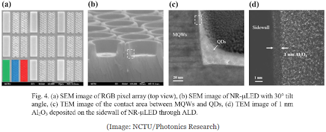
Researchers from Taiwan’s National Chiao Tung University, China’s Xiamen University and SIJ Technology have developed a monolithic Micro LED which achieves full-color display. Through the adoption of ALD, the thin layer between multiple quantum wells and quantum dots of NR Micro LED can be controlled and nonradiative resonant energy transfer (NRET) for color conversion can be maintained (LINK).
 
Micro-LEDs are a strong challenger to existing display technologies such as LCDs (liquid crystal displays), OLEDs (organic light-emitting diodes) or conventional LEDs (light-emitting diodes). Offering compact size, low power consumption, superior brightness, and energy efficiency, higher contrast and color saturation, ultra-high resolution, flexibility, and excellent reliability, micro-LEDs are currently actively studied and developed at the leading electronics manufacturers and R&D institutes around the world. Micro-LEDs are typically used for small screens such as those used in tablets, smartphones, and smartwatches, and the first large area displays have also been demonstrated already.


The Co-Lab collaboration signature ceremony of NCTU and Finland Picosun 2015 (LINK)
 
Still, the micro-LED technology has certain drawbacks that hinder its full-scale commercial breakthrough. The micro-LED screen consists of minuscule pixels producing green, blue and red light. Some steps in the manufacturing process of these pixels easily cause damage to their delicate nanometer-scale structures, which leads to loss of light intensity. ALD has now been proven to effectively fix these damages, not only restoring the light intensity but actually boosting it to superior levels. At Picosun customer site, National Chiao Tung University (NCTU), Taiwan, the light-emitting intensity of micro-LEDs has been enhanced by 143.7% by using ALD passivation layers deposited with PICOSUN™ ALD equipment(*).

“We are happy to report these great results achieved in micro-LED efficiency enhancement using ALD technology. PICOSUN™ ALD equipment has been an integral part of our facilities for a long time, and we are always impressed by their performance and the superior ALD film quality obtained with them. Picosun’s customer support is also impeccable, which is very much appreciated considering we collaborate extensively with industries. Whenever we need something regarding the equipment or process consultancy, Picosun staff is always up to date and ready to provide thorough answers,” states Professor Hao-Chung Kuo from NCTU.

“NCTU is our prestigious customer and a key partner for years already. We are glad that our ALD solutions have enabled this impressive performance boost to their micro-LEDs. Micro-LED technology has immense potential to disrupt the solid-state lighting market and our Asian customers, both in industries and R&D, will surely lead the forefront of this development,” continues Mr. Edwin Wu, CEO of Picosun Asia Pte. Ltd.

Monday, March 25, 2019

Picosun’s high aspect ratio ALD enables 3D thin-film batteries

ESPOO, Finland, 25th March 2019 – Picosun Group, a leading supplier of advanced ALD (Atomic Layer Deposition) thin film coating technology for industrial production, reports excellent results in conformal ALD coatings for solid-state 3D thin-film batteries.

Solid-state thin-film batteries are increasingly needed in portable and wearable electronics such as smartphones, tablets, smart watches, autonomous sensors, and also in implantable medical devices. These batteries have to combine small, compact size with high energy density, which is why the next step is to move away from planar battery geometry to a three-dimensional one. In 3D thin-film batteries, nanostructured, corrugated high aspect ratio (HAR) structures multiply the active surface area and thus the battery’s charge storage capacity. 
 

Advanced manufacturing methods are called for to produce the functional layers such as electrodes and solid electrolyte inside these structures. ALD is able to create the highest quality conformal material layers inside HARs even as high as 1:3000, so it shows great potential for 3D thin-film battery manufacturing. Picosun’s high aspect ratio ALD is already utilized in various semiconductor and MEMS applications on an industrial scale, and now it has been successfully used in manufacturing solid-state 3D thin-film battery electrodes. Excellent results have been achieved already with the standard PICOSUN™ ALD reactor configuration with optimized process parameters, but for even more challenging HAR coating needs, Picosun’s patented Picoflow™ diffusion enhancing technology is ideal.

“The skyrocketing popularity of portable and wearable electronics creates a demand for compact and embeddable energy sources to power these devices. Solid-state 3D thin-film batteries are a strong candidate for this, and we at Picosun are happy to introduce our ALD solutions to the manufacturers. It is notable that even with our basic ALD we are able to create the functional layers with the highest conformality inside the batteries’ challenging HAR structures, and our approach is readily scalable to high volume industrial production. And, when these structures get even more complicated on nano-scale, our Picoflow™ technology is there to guarantee top quality deposition results with industry-proven reliability,” summarizes Mr. Juhana Kostamo, Managing Director of Picosun Group.

Monday, February 25, 2019

Picosun’s ALD yttria eliminates corrosion in demanding applications

ESPOO, Finland, 25th February 2019 – Picosun Group, a leading supplier of ALD (Atomic Layer Deposition) thin film coating solutions for global industries, has developed an excellent quality ALD yttria process for corrosion protection in harsh environments.

Yttria, aka yttrium oxide, Y2O3, is extremely hard, dense, and mechanically strong material which has excellent chemical and erosion resistance and very high melting point. These characteristics make it ideal for protective coatings in applications where operating conditions are extreme. Some examples of these applications are various semiconductor production equipment and metal production. Y2O3 also finds uses as a high-k gate dielectric in novel microelectronics such as carbon-based components, thin film transistors, and germanium-metal-oxide semiconductors. 
 
A street in Sweden close to the Ytterby mine, famous for having the single richest source of elemental discoveries in the world; the chemical elements Yttrium (Y), Ytterbium (Yt), Erbium (Er) and Terbium (Tb) are all named after Ytterby (photo from Miras Miarakel LINK)
 
Yttrium oxide coatings are typically produced with physical vapor deposition, electron beam evaporation, or sputtering methods, but ALD offers several advantages over these techniques. ALD-manufactured yttria films are intrinsically pinhole-free, extremely dense, ultra-thin, and highly uniform, and they cover conformally even the smallest nanoscale details, voids, crooks, and steps on the surface. Achieving these properties with a fraction of film thickness compared to traditional methods saves costs and materials. As the ALD process is based on spontaneous surface chemical reactions between gaseous reactants, it is gentle to the coated surface and can be applied at moderate temperatures, if needed. Cost-efficient, high throughput production of yttrium oxide coatings can be realized in Picosun’s industry-proven PICOSUN™ P-1000 and P-300B ALD equipment (*).

“Our high volume production ALD machinery such as PICOSUN™ P-1000 and P-300B reactors has been a huge success since their launch. With this equipment we have been able to take ALD to totally new application areas in e.g. surface protection and functionalization of various mechanical components, anti-tarnish and decorative coatings for coins and watch parts, and production of biocompatible coatings for medical devices. Now, our superb quality yttria process, upscaled to production in our high volume reactors, enables revolutionary ALD solutions in industries where durable and reliable surface protection against extreme conditions is needed,” states Dr. Jani Kivioja, CTO of the Picosun Group.

Thursday, February 21, 2019

Picosun’s ALD encapsulation prevents electronics degradation

ESPOO, Finland, 14th February 2019 (LINK) – Picosun Group, a leading supplier of ALD (Atomic Layer Deposition) thin film coating solutions for global industries, reports unprecedented results in high reliability electronics protection with ALD.

Hermetic encapsulation by ALD nanolaminates developed by Picosun has been proven to block tin whisker formation on PCB (printed circuit board) assemblies completely(*). During the observation period of over one month to three years, ALD-protected samples showed no tin whisker growth at all, whereas on non-protected samples tin whisker density of over 1000 pcs/cm2 was measured. In addition to blocking tin whiskering, Picosun’s ALD nanolaminates help to protect the PCBAs against other key degradation phenomena such as various forms of corrosion and oxidation. Hermetic ALD coating works efficiently even against moisture and gaseous sulfur in polluted atmosphere. Due to its nanometer-scale thickness, the ALD film has no effect on the PCBA functionality, mass or dimensions and it allows reworking of the PCBA. 
 

Tin whisker formation and corrosion are particularly fatal in several high reliability electronics applications such as data centers, space, aviation, military, medical and industrial control systems. Picosun’s revolutionary ALD encapsulation method offers now safety improvement, product lifetime lengthening, and even long-term cost savings to these manufacturers. Fast, cost-efficient processing of large amounts of PCBAs can be realized in PICOSUN™ P-1000 and P-300B high volume batch ALD systems with production-proven, industry-optimized processes.


“We are happy to announce these groundbreaking results obtained with our ALD encapsulants in protection of specialty electronics. This is a new, potentially huge market for ALD. There has already been lots of interest towards our turn-key coating solutions for large scale PCBA protection from the corresponding industries. This shows again the versatility of ALD and its power to disrupt near all fields of today’s industrial manufacturing”, says Dr. Jani Kivioja, CTO of Picosun Group.