


%20(1).png)
Researchers led by TSMC R&D Europe B.V. in Leuven Belgium (Imec) and Lund Sweden (Lund Nano Lab), claim the first
demonstration of an unstrained indium arsenide (InAs) fin field-effect
transistor (finFET) with 20nm fin height (Hfin)
[R. Oxland et al, IEEE Electron Device Letters, published online 29 January 2016]. The team also included researchers from University of
Glasgow in the UK, Texas State University in the USA, and TSMC in
Taiwan.
The gate insulation consisted of 5nm ZrO2 deposited by ALD, yielding an 1.2 nm equivalent oxide thickness (EOT).
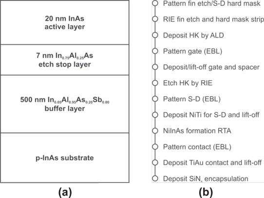
(a) Layer structure used, showing the pseudomorphic InAlAs etch-stop
layer and (b) process flow for fabrication of InAs finFETs, starting
with first step after wafer growth. (Figure from Semiconductor Today)
Full story here by Mike Cooke in Semiconductor Today and the IEEE Electron Devices abstract below.
InAs FinFETs with Hfin = 20 nm fabricated using a top-down etch process
Oxland, R. Li, X. ; Chang, S. ; Wang, S. ; Vasen, T. ; Ramvall, P. ; Contreras-Guerrero, R. ; Rojas-Ramirez, J. ; Holland, M. ; Doornbos, G. ; Chang, Y. ; Macintyre, D. ; Thoms, S. ; Droopad, R. ; Yeo, Y. ; Diaz, C. ; Thayne, I. ; Passlack, M.IEEE Electron Device Letters, published online 29 January 2016
We report the first demonstration of InAs FinFETs with fin width Wfin in
the range 25–35 nm, formed by inductively coupled plasma etching. The
channel comprises defect-free, lattice-matched InAs with fin height Hfin
= 20 nm controlled by the use of an etch stop layer incorporated into
the device heterostructure. For a gate length Lg = 1 nm, peak
transconductance gm,peak = 1430 µS/µm is measured at Vd = 0.5 V
demonstrating that electron transport in InAs fins can match planar
devices.
No comments:
Post a Comment