


%20(1).png)
Graphene has a big problem - it lacks a bandgap which is needed for many electronic devices and this has led searching of alernate 2D materials. Most focus today is on transition metal dichalcogenides
(TMDs). One of the most promising TMDs is molybdenum disulfide (MoS2) with a bandgap (∼1.2 eV) for bulk MoS2 and a direct bandgap (∼1.8 eV) in the mono layer form monolayer.
Some weeks ago it was reported that ALD sales booming for Arradiance GEMStar XT line. Here is an Open Source paper in JVSTA on depositing 2D MoS2 by alternate pulsing of MoCl5 and H2S on 6 inch wafers using an Arradiance GEMStar ALD reactor by School of EECS, Oregon State University and Sharp Lab of America.
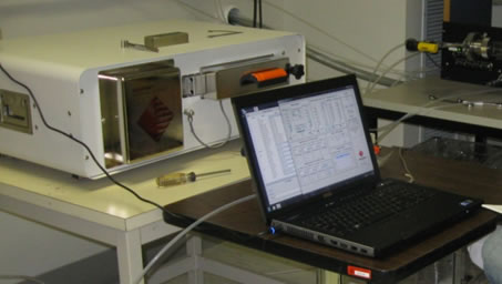
Installed Fall 2010: Arradiance Gemstar (see press release);
150mm ALD reactor with 3D substrate capability, in-situ quartz crystal
microbalance, and 5 precursor source lines (1 gas; 2 vapour draw for
liquids; and 2 low vapor pressure sources, heated up to 120C, one with
N2 boost)
Here you can find more details on the research and facilities of Prof. John F. Conley`s Novel Materials and Devices Group at Oregon State: http://web.engr.oregonstate.edu/~jconley/facilities.html. In Addition to the Arradiance GEMStar they are operating a Picosun SUNALE R-200 200mm Plasma Enhanced ALD system.
Atomic layer deposition of two dimensional MoS2 on 150 mm substrates
J. Vac. Sci. Technol. A 34, 021515 (2016); http://dx.doi.org/10.1116/1.4941245
Low temperature atomic layer deposition(ALD) of monolayer to few layer MoS2 uniformly across 150 mm diameter SiO2/Si and quartz substrates is demonstrated. Purge separated cycles of MoCl5 and H2S precursors are used at reactor temperatures of up to 475 °C. Raman scattering studies show clearly the in-plane (E12g) and out-of-plane (A1g) modes of MoS2. The separation of the E12g and A1g peaks is a function of the number of ALD cycles, shifting closer together with fewer layers. X-ray photoelectron spectroscopy
indicates that stoichiometry is improved by postdeposition annealing in
a sulfur ambient. High resolution transmission electron microscopy
confirms the atomic spacing of monolayer MoS2 thin films.
No comments:
Post a Comment