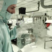
Save the date! On June 9th 2022, we will organize a spatial ALD day at the Eindhoven University of Technology.
— AtomicLimits (@AtomicLimits) April 6, 2022
You can preregister on the website! The final registration form will appear early May when the detailed program is known.https://t.co/GjjpkGRdDX#ALDep #ALD pic.twitter.com/Bt5jJYg111
Showing posts with label Spatial ALD. Show all posts
Thursday, April 7, 2022
Spatial ALD Day coming up at TU Eindhoven June 9
Tuesday, April 5, 2022
Innovative Spatial ALD system at the LZH can precisely coat complex-shaped optics
New possibilities: The LZH can also coat curved optics uniformly with the innovative Spatial ALD system. This is interesting, for example, for applications in the automotive lighting sector. The system achieves high deposition rates.Thanks to the plasma-based Spatial ALD system, another application that is in high demand in industry has been made economical. Layer systems of uniform thickness can be developed and manufactured much faster than before on curved and structured optics.
The system was developed by the Finnish company Beneq together with the LZH.
Press release: Innovative Spatial ALD system at the LZH can precisely coat complex-shaped optics | Laser Zentrum Hannover
Sunday, October 31, 2021
Nanofabrication via Maskless Localized Atomic Layer Deposition of Patterned Nanoscale Metal Oxide Films
Here is a cool demonstration of direct write Spatial ALD or LOCALD like the researches at Laboratoire des Multimatériaux et Interfaces, University of Lyon is calling it.
Nanofabrication via Maskless Localized Atomic Layer Deposition of Patterned Nanoscale Metal Oxide Films
ACS Applied Nano Materials (IF5.097), Pub Date : 2021-10-18, DOI: 10.1021/acsanm.1c02550
Laabdia Midani, Waël Ben-Yahia, Vincent Salles, Catherine Marichy
A modified open-air spatial atomic layer deposition (SALD) head is employed to fabricate complex oxide patterns on various substrates. The co-reactant being kept in the surrounding atmosphere, a simple injection head that consists of three concentric nozzles with only one precursor outlet has been designed. Easy and reversible modification in the diameter of the metal precursor outlet permits direct patterning with different lateral sizes. Maskless deposition of uniform and homogenous TiO2 and ZrO2 thin films is successfully demonstrated with a lateral resolution tuned from millimeters to hundred micrometers range while keeping the film thickness in the range of a few to hundreds of nanometers with a control at the nanoscale. This localized SALD approach, named LOCALD, also enables layer stacking and deposition on structured substrates.
Supporting information: an1c02550_si_001.pdf
Tuesday, April 20, 2021
Spatial atomic layer deposition system FHR.Star.400x300-SALD delivered
FHR (Press Release) has successfully delivered the FHR.Star.400x300-SALD. This is FHR’s first machine using spatial atomic layer deposition (spatial ALD). The system is capable of depositing films on both 200 mm wafers and textiles or other 3D substrates of up to 400 x 300 x 10 mm³.
Spatial ALD allows for high speed and highly conformal coatings on flat as well as micro-structured surfaces. Applications are dielectric layers for anti-reflective coatings on lenses as well as coatings for electrical insulation or protection against moisture or oxygen applied to energy systems, medical devices or functionalized textiles.
In its base configuration, the FHR.Star.400x300-SALD is made for thermal ALD on up to eight wafers or four 3D substrates in parallel. For Al2O3 on wafers, deposition rates of 5-10 nm/min and thickness non-uniformities <± 2.0% have been reached. A large blind flange allows to add other thin film technologies or plasma treatment and the machine is already prepared to for in-situ ellipsometry and transmission spectroscopy for improved process control. To further increase the productivity, the FHR.Star.400x300-SALD can be included in a cluster setup with a central handling robot chamber, load locks, pre-treatment chambers or other process chambers.
FHR, Marian Böhling (CSO): „ALD coating technology is valued for its unique conformality and precision even on 3D substrates but claimed to be slow and therefore often ignored. Our FHR.Star.400x300-SALD refutes this claim impressively and makes ALD available as an exciting and promising thin film technology for a wide range of industrial applications. Installed at a world-class thin film research institute, this FHR.Star.400x300-SALD offers a low-threshold access for everybody interested in using ALD for own products.“
FHR Anlagenbau GmbH - The Thin Film Company was founded in 1991 and offers tailor-made vacuum coating systems and sputtering targets as well as coating and equipment service from a single source.
The close cooperation with our customers starts with the process development and continues with the development of pilot scale up to mass production. Our portfolio integrates the technologies sputtering, evaporation, PECVD and ALD into the equipment types cluster, inline, roll-to-roll and batch. Based in Germany and with systems installed worldwide in various industries such as semiconductors, MEMS, electronics, sensor technology, optics, photovoltaics, etc., we will jointly find vacuum coating solution for our customers.
Contact
FHR Anlagenbau GmbH
Marketing & Communication
Phone: +49 35205 520-0
E-mail: marketing@fhr.de
Monday, April 12, 2021
Spatial Atomic Layer Deposition (SALD): Essential for today's and future battery production
SALD is a carve-out of the brainport Eindhoven-based OEM company SoLayTec, which develops and sells advanced spatial ALD machines specifically for mass-produced solar cells. Because there were a lot of requests for applications other than solar cells, the company SALD was founded in 2019. In the relatively short time in which the company has existed, it has already succeeded in implementing the complex technology in a compact machine that serves for research purposes and small-scale production of spatial ALD layers.
The full story can be found here published by Brainport, NL: LINK
Background: In 2008 TNO scientists developed a brilliant solution for this: Spatial ALD. With this new technology, TNO was able to increase the production speed 5 to 10 times, while the coating quality remained the same. This led to the establishment of SoLayTec, which developed and sold advanced Spatial ALD machines for the mass production of solar panels. This makes SoLayTec the only company with large-scale production experience within the emerging world of Spatial ALD. The in-depth expertise in Spatial ALD technology, combined with the unique ability to transfer it from lab to fab, offers great opportunities in today's growth markets. That is why a new company has been set up alongside SoLayTec, with the ambition to be at the forefront of promising new applications of Spatial ALD. The name chosen is the worldwide abbreviation for this innovative technology: SALD.
Monday, November 16, 2020
Dutch SALD and German Fraunhofer to develop Spatial ALD technology for production of 1,000 km range EV battery modules
Several reports state that Dutch SALD, a subsidiary of SoLayTec, and German Fraunhofer have jointly developed a Spatial ALD (SALD) technology for producing EV batteries that aim at 1,000 km range.
Not too many details are available at this point, please check SALD below for further details
SALD: LINK
From SALD Webpage: Li-ion batteries are indispensable for consumer electronics and electric vehicles, and it is vital that the safety, longevity and capacity of these batteries is maximized. Spatial ALD can assist in this. For common Li-ion batteries that comprise liquid electrolytes, ALD can be used to prepare the solid-electrolyte interphase (SEI). This artificial SEI - typically about a nanometer in thickness - protects the anode or cathode active materials (CAMs) from the electrolyte, enhancing the long-term stability and safety of the Li-ion battery.
Friday, September 18, 2020
SALD deposits trust in new advisory board chaired by Prof. Kessels
Spatial atomic layer deposition equipment manufacturer SALD has set up an advisory board, which, apart from acting as a sounding board to management, will also have an ambassadorial function
The advisory board is chaired by Prof. Erwin Kessels, leader of the Plasma & Materials Processing group at Eindhoven University of Technology. He’s joined by marketing consultant John Niemeijer of The Brandhouse, innovation consultant Peter Visser of Innovisser and accountant Werner Vervest of Vervest Financial Services.
Full article: SALD deposits trust in new advisory board (LINK)
Prof. Erwin Kessels was the Awardee of the AVS 2019 ALD Innovator award “For Original Work and Leadership in ALD" (https://ald2019.avs.org/awards/)
Sunday, November 17, 2019
Holst Centre showcase spatial atomic layer deposition (sALD) for thin-film transistor (TFT) backplane
Researchers from Holst Centre have become the first to use spatial atomic layer deposition (sALD) to create both the semiconductor and dielectric layer in a thin-film transistor (TFT) backplane. Using a low-temperature, large-area process for the backplane, the team created a 200 ppi QVGA display demonstrator. The process allows TFTs to be produced on cheaper, transparent plastic foils, significantly reducing the cost of flexible electronics applications such as displays and image sensors. To showcase the technology, Holst Centre has produced a display demonstrator using a backplane of top-gated self-aligned TFTs on a PEN foil. The display is being presented at the International Display Workshop (IDW) in Sapporo, Japan from November 27-29.
|
The backplane was produced at temperatures below 200 °C, achieving mobilities of 8 cm2/Vs in transistors with channel lengths down to 1 μm. It was then combined with an OLED frontplane to create a 200 ppi QVGA display.
The demonstrator was produced using sALD equipment initially developed by Holst Centre and which is currently being commercialized by the start-up SALDtech. Spun out from Holst Centre in 2018, SALDtech offers the only sALD tools for Gen 1 (32 x 25 cm) substrate size flat-panel displays currently available. Earlier this year, it received a second round of investment to develop and build production equipment that could be integrated into the production lines of next-generation flexible OLED displays for mobile phones, tablets, TVs and more.
“We are already delivering TFT performance with sALD that is comparable with the best sputtered devices. And through additional optimization of processes and materials, there is considerable room for further improvements. At the same time, we are looking at producing all TFT layers with sALD to further simplify and reduce the cost of high-volume flexible TFT manufacturing,” says Ilias Katsouras, Senior Scientist at Holst Centre.
Many flat-panel displays today use the semiconductor indium gallium zinc oxide (IGZO) in the TFT backplane. IGZO is usually deposited via sputtering and requires a high-temperature anneal procedure to ensure performance. This high-temperature step necessitates substrates with high melting points, which are typically more expensive.
Developed by Holst Centre, large-area sALD is an atmospheric-pressure technique that allows ultra-thin layers of materials to be deposited quickly with high compositional control and excellent thickness uniformity. The technique has previously been used to produce high-quality individual layers of materials for solid-state batteries and TFT backplanes. Now, for the first time, Holst Centre has used sALD to deposit both the IGZO semiconductor layer and the aluminum dielectric-oxide dielectric layer in an integrated TFT process onto a low-cost, transparent plastic foil.
Using a single technique to produce multiple layers of material offers flexible TFT manufacturers the possibility of improving both production throughput and the interface between layers, which in turn increases device performance.
Wednesday, May 22, 2019
SALDtech receives further funding to enable mass production of the next generation foldable OLED displays
SALDtech speeds up commercialization of Spatial Atomic Layer Deposition equipment for the display industry
Eindhoven, 22 May 2019 - SALDtech announced today that it has closed a second investment round with Innovation Industries, a leading high-tech VC fund and BOM, Brabant Development agency. TNO, through its subsidiary Holst Centre, has invested over 10 years in developing a new technology called Spatial Atomic Layer Deposition to produce large area ultra-thin layers with world class performance. SALDtech, a spin-off of TNO, will use the investment to develop and build production equipment to be integrated into the production lines of next generation flexible OLED displays for mobile phones, tablets, TVs and more.
(Photo: TNO)
“We are very pleased with this investment as it enables us to further develop our product and speed up our sales” Huib Heezen, CEO of SALDtech states: “SALDtech will continue to cooperate closely with TNO on process innovation and will use the expertise on high tech equipment as readily available in the Eindhoven area for our product development. We are delighted to now have two top Dutch investors in the form of Innovation Industries and BOM on board who are committed for the long term.”
“We are excited that we have been a part of SALDtech since its first round last year and that we can continue to support SALDtech’s growth by participating also in this financing round”, says Nard Sintenie, Partner at Innovation Industries. “SALDtech’s technology has the ability to change the way we are working and interacting with displays and thereby addresses a huge market.”
“SALDtech has the potential to become the leading supplier in the display market” according Jurgen Van Eck, Senior investment manager at BOM Brabant Ventures“ As such, the company will play an important role towards local suppliers. We are happy we are able to contribute towards the further development of SALDtech”
Founding institute TNO is delighted with the opportunity this second financing round offers to SALDtech. “Both Innovation Industries and BOM have multiple investments in TNO spin-offs, , which shows the potential of the research we are doing at Holst Centre and TNO for the Dutch high tech industry. This investment is the next step in strengthening the Dutch economic position and Brainport in particular.” says Jaap Lombaers, Director at TNO.
About SALDtech
SALDtech BV is a spinoff from the Netherlands Organisation for Applied Scientific Research (TNO) and is based in Eindhoven, The Netherlands. The company was founded in 2018 to further develop, build and sell commercial Spatial Atomic Layer Deposition (SALD) systems into the flat panel display industry. The SALDtech tool will help enable the production scale up of next generation display technologies. Related end product display markets include smartphones, tablets, TV’s as well a new form factor displays in (autonomous) cars and on practically every surface.
Contact:
Huib Heezen (CEO)
huib.heezen@saldtech.com
+31 (0)6 30615028
Saturday, April 6, 2019
Amtech Systems plans to divest its solar businesses
Amtech Systems, a manufacturer of capital equipment and consumables used in fabricating semiconductor devices, LEDs, SiC and silicon power chips ans well as solar cells, is planning to sell its solar businesses.
Amtech management and Board of Directors have decided to focus solely on growth opportunities in the Company’s semiconductor and SiC/LED polishing businesses and intend to sell the Company’s solar businesses, including its Tempress and SoLayTec subsidiaries.
Amtech’s J.S. Whang, Chairman and Chief Executive Officer, commented, “In November 2018 we announced that we had initiated a comprehensive review of our solar businesses. In a February update we noted thus far our review strongly indicates that our combined Semi and SiC/LED polishing business provide better markets for enhancing the value of Amtech Group. We have recently completed our assessment and conclude, along with Tempress and SoLayTec management, that significant investment is required to effectively compete in the changing solar industry. We therefore conclude Tempress and SoLayTec would be better positioned to capitalize on opportunities in the solar industry under new ownership.”
Source: Evertiq LINK
Monday, December 17, 2018
High Speed Batch Atomic Layer Deposition using Vortex ALD by Lotus Applied Technology
Here is a cool animation on the Lotus High Speed Batch Atomic Layer Deposition using Vortex ALD.
YouTube.com
Founded in 2007, Lotus Applied Technology was formed through a spinoff of the thin film process group within Planar Systems, Inc., a pioneer in Atomic Layer Deposition technology and manufacturing. Housed in a fully dedicated 20,000 square foot thin film processing and R&D facility in Hillsboro, Oregon, the team of technologists has been working together for over 20 years, developing innovative solutions to thin film processing challenges. Their equipment set includes a wide array of thin film deposition, lithography, and patterning equipment, including a versatile set of ALD equipment:
- Six P400 Conventional Pulse-Based Batch ALD reactors
- Roll to Roll ALD Research Scale Reactor
- TransFlex Roll to Roll ALD Pilot Scale Reactor
- Vortex Rotary Batch Reactor
Tuesday, March 13, 2018
SoLayTec ships new ALD order to Asia for PERC cell manufacturing
North American Clean Energy reports (LINK): Amtech Systems, Inc. (NASDAQ: ASYS), a global supplier of production equipment and related supplies for the solar, semiconductor, and LED markets, announced its solar subsidiary, SoLayTec B.V., has shipped a next generation solar Atomic Layer Deposition (ALD) to an Asian customer. While the PV market is shifting towards high efficiency cell designs, production with high yield, A-grade cells, is getting increasingly important.
Fokko Pentinga, CEO and President of Amtech, commented, "For this project we are delivering the equipment for the PERC line upgrade and assisting the customer with the PERC ramp-up and line integration. PV manufacturers are experiencing extreme price pressure, resulting in an increasing need for higher cell quality with narrow cell efficiency distribution. The highest line yield possible of A-grade cells is essential to ensure good margins for these advanced production lines. Al2O3 wrap-around during deposition will result in reduction of the cell efficiency by as much as 0.2%, as well as front side color variations. Our ALD equipment addresses PV manufacturers' challenges, by delivering the highest PERC cell efficiency using Al2O3,, highest A-grade cells, and stable deposition process without any wrap around. Another challenge we address for A-grade cells is scratch free manufacturing of SiNx deposition for rear-side capping and front-side ARC. Our scratch free solution using our direct-plasma PECVD equipment is gaining momentum, with shipments and order backlog totaling more than 1GW."
Saturday, February 10, 2018
Spatial atomic layer deposition for coating flexible porous Li-ion battery electrodes
Here is important step forward in fast roll to roll processing of Li-battery electrodes using fast spatial ALD from CU Boulder, Colorado. Spatial ALD (SALD) is based on separating the precursors and inert gas purges in space rather than in time and therefore the deposition rates up to a hundred times faster are achievable. SALD can be performed at ambient atmosphere and therefore is a cheaper technology due to less need of expensive vacuum technology compared to conventional low pressure ALD.
High speed and low cost of ownership opens the door to high volume manufacturing of bulk quantities of energy materials for applications including solar energy, energy storage, or smart windows. Previously ALD Nanosolutions has announced a Spatial ALD technology for conformal encapsulation of ALD on powder material like for instance Li-battery cathode powder (LINK). A good overview of Spatial ALD for energy applications is this review paper by David Muñoz-Rojas et al: "Spatial Atomic Layer Deposition (SALD), an emerging tool for energy materials. Application to new-generation photovoltaic devices and transparent conductive materials" https://doi.org/10.1016/j.crhy.2017.09.004 [OPEN ACCESS]
Please find the JVSTA abstract below for the recent article form Boulder:
Spatial Atomic Layer Deposition for Coating Flexible Porous Li-Ion Battery Electrodes Abstract for paper @GeorgeGroupCU @@coschoolofmines https://t.co/eCCJEdudwa pic.twitter.com/K2R6P7i6tc— JVST A - JVST B (@JVSTAB) February 7, 2018
Friday, December 15, 2017
Amtech Announces Follow-On Order for Next Generation Solar ALD for PERC Cell Line
TEMPE, Ariz., Dec. 14, 2017 /PRNewswire/ -- Amtech Systems, Inc. (NASDAQ: ASYS), a global supplier of production equipment and related supplies for the solar, semiconductor, and LED markets, today announced its solar subsidiary, SoLayTec B.V., has received a follow-on order for three next generation solar Atomic Layer Deposition (ALD) systems. The order is expected to ship and be installed in this fiscal year. As a leading ALD supplier in the market, SoLayTec has booked a total of 25 ALD system orders since its inception, of which 15 will be used in mass production.
Depending on the capacity levels that are needed, SoLayTec offers three
types of InPassion ALD. The main difference is the number of deposition
units modules added in such a system. The basic three products offered
are 4, 6 or 8 deposition units, which result in 2,400 wph, 3,600 wph or
4,500 wph respectively. (www.solaytec.com)
Fokko Pentinga, CEO and President of Amtech, commented, "This follow-on order brings the total ALD tools ordered by this specific customer to seven. Four systems have been put in production of PERC solar cells in the second half of fiscal 2017. The orders SoLayTec has received from this particular customer represent a total of 1GW of PERC production capacity. This follow-on order validates our customer's confidence in the performance capabilities of our spatial ALD system in high-volume production of PERC solar cells. There is a high level of enthusiasm in the PV marketplace for PERC solutions and this manufacturing platform supports our customers' goals to improve the total cost of ownership by increasing cell efficiency."
Sunday, March 19, 2017
Meyer Burger offer high-speed Spatial ALD Technology for R2R Production
Meyer Burger has updated their ALD Equipment offering and are now offering two ALD Products, one for R&D and one for Production. Both are based on Spatial ALD coating technology.
The FLEx S2S sALD
The FLEx S2S sALD is suitable for application development that require high speed ALD coating technology combined with excellent uniformity (Source: Meyerburger.com)
The FLEx S2S sALD (sheet to sheet spatial ALD coating solution) is suitable for application development that require high speed ALD coating technology combined with excellent uniformity. The developed process is transferrable to the FLEx R2R sALD (roll to roll spatial ALD coating solution) industrial Equipment.
Main advantages
- Grow rates > 1 nm/s; 100 times compared to conventional ALD
- Flexibility in substrate material and layer thickness
- No pinholes
- Thickness control on atomic scale
- No gas phase reaction. No parasitic deposition
- Excellent conformity
- High application potential in flexible electronics, photovoltaics, OLED
- No vacuum process, process at atmospheric pressure
- Compact footprint
FLEx R2R sALD'
The FLEx R2R sALD is a full scale machine for high speed production on foil.
Wednesday, December 14, 2016
High-Throughput, Cost-Effective Deposition via Atmospheric Pressure Spatial Atomic Layer Deposition
Here is a new paper on atmospheric Spatial ALD from Kevin Musselman and co-workers at University of Waterloo in Canada. According to information at The Waterloo Institute for Nanotechnology web: "Musselman helped pioneer the use of atmospheric pressure spatial atomic layer deposition (AP-SALD) thin films in optoelectronic devices. He used these films to address key questions in the field of energy conversion and to develop new optoelectronic devices. Musselman produced thin films of metal oxide alloys with tunable optoelectronic properties with which he probed loss mechanisms in colloidal quantum dot solar cells, ‘hybrid’ polymer-oxide solar cells and light emitting diodes, and all-oxide solar cells. These metal oxide films were also used to produce new, colour-pure “hybrid” organometal halide perovskite light-emitting diodes."
Nanomanufacturing: High-Throughput, Cost-Effective Deposition of Atomic Scale Thin Films via Atmospheric Pressure Spatial Atomic Layer Deposition
Kevin P. Musselman, Chukwuka F. Uzoma, and Michael S. MillerChemistry of Materials 2016 28 (23), 8443-8452
DOI: 10.1021/acs.chemmater.6b03077
Up&Coming perspective by K. Musselman @WaterlooENG on high throughput, atm pressure, roll-to-roll #ALDep https://t.co/77Gs6xaYQW pic.twitter.com/jLSboZSz6h— Chem of Materials (@ChemMater) December 13, 2016
Friday, November 25, 2016
The ALD Passivation Market for Solar Cells is Evolving
Levitech Reports: Almere, the Netherlands – November 23, 2016 – The ongoing evolution
from Al BSF cells to new PERC and n-type cell concepts will continue in
the coming years. This production shift is made possible by the
development of high volume capable Al2O3 deposition systems. The
intrinsic properties of ALD are a perfect match with the requirements
from cell design and technological point of view, both for PERC as well
as n-type cells. Additionally, ALD systems result in a proven CoO
benefit as compared to PECVD due to the increased maintenance interval
and its beneficial effect on cell efficiencies.
从 Al BSF 电池到新型 PERC 和 n
型电池概念的持续演进将在未来的几年 中继续保 持下去。高產量 Al2O3 沉积系统 的发展推动了这一生产转变。从电池的设计 和 技 术 的 角 度
来 讲 ,无 论 是 PERC 还是 n 型电池,ALD 的固有属性可谓正应所需。除 此 之外,鉴于 ALD 系统可以增加维修间隔
并改善电池效率,它还能够带来 PECVD 不 具备的实际 CoO 益处。
Novel high-speed ALD outperforms current techniques for making displays
The Holst Centre in the Netherlands reports: Fast and industry-compatible, spatial atomic layer deposition (sALD) promises to revolutionize production of thin-film displays. Now researchers at Holst Centre have shown that sALD can deliver semiconductor layers with better performance than physical vapor deposition (PVD) at the same – and potentially even higher – throughputs. An easily scalable, atmospheric-pressure process, sALD could soon become the preferred method for creating large-area thin-film and flexible devices.
A key step in producing next-generation ultra-high definition) displays is the creation of a highly uniform layer of an amorphous oxide semiconductor such as indium-gallium zinc oxide (IGZO). Today, this is typically done using a PVD technique known as sputter deposition. Sputtering requires expensive vacuum equipment and can also prove difficult to correctly control material composition and thickness over large areas. This results in variable transistor performance, particularly in thin film applications such as displays.
Now Holst Centre has shown that sALD offers an industry-compatible alternative which improves display performance and at the same time could cut production costs. The team has used the technique to create semiconductor layers with charge carrier mobilities (a key measure of semiconductor performance) of 30 to 45 cm2/Vs. This compares to typical mobilities around 10 cm2/Vs for sputtering. The sALD layers also exhibited low off current, switch-on voltages around 0 V and excellent bias stress stability.
"Spatial ALD offers all the performance advantages of traditional ALD – superior control of layer thickness and composition, large-scale uniformity and unparalleled conformability – but at 10-100 times the speed. So a typical 50-nm thick layer can be produced within the standard 1 minute window demanded by today's industrial processes," said Paul Poodt, Program Manager sALD at Holst Centre.
"The performance of sALD means semiconductor layers could become much thinner, enabling even higher throughputs and lower material consumption," added Gerwin Gelinck, Program Director Flexible and Large Area Transistor Electronics at Holst Centre. "In fact, its performance characteristics are preserved even when scaling down the semiconductor thickness to less than 5 nm. This can lead to novel semiconductor structures, such as super-lattices, with even higher electron mobilities."
The Holst Centre team and partners are now taking steps towards the upscaling and commercialization of these sALD processes and related equipment.
Monday, November 14, 2016
Tutorial on Fast Spatial Atmospheric ALD by David Muñoz-Rojas from LMGP-CNRS
We are happy that Dr. David Muñoz-Rojas from LMGP-CNRS, Grenoble will come to Dresden in January 17th 2017 to give a Tutorial at ALD for Industry on Spatial ALD "Speeding up the unique assets of ALD". Until then please enjoy this recent presentation available on Youtube - pretty amazing stuff!
Dr. David Muñoz-Rojas - Laboratoire des Matériaux et du Génie Physique
(LMGP) Université Grenoble Alpes, Grenoble, France - presents a Waterloo
Institute for Nanotechnology (WIN) seminar titled: "Atmospheric
Pressure Spatial Atomic Layer Deposition (AP-SALD): a new technique
allowing the fast and scalable “printing” of functional oxides" (Embedded Youtube)
Thursday, November 10, 2016
BENEQ ALD process beats PVD in speed, quality and cost of ownership
Readers of this blog has probably noticed that ALD is continuously taking market shares from PVD and is growing much faster than PVD. ALD is a disruptive technology in many ways especially in semiconductor manufacturing. Now BENEQ Spatial Plasma ALD process also beats PVD in speed, quality and cost of ownership for Anti Reflection coatings!
High-performance AR coatings for mass production 08.11.2016 | BENEQ Equipment : Ever since we earlier this year announced the licensing of rotary spatial ALD technology and launched Beneq R11, our new rotary tool for plasma enhanced spatial ALD, we have received a steady flow of inquiries and questions about where we see the new equipment being the most useful. Plenty of things, we might say, but here is one prime example: fast low temperature optical coatings, such as anti-reflection (AR) coatings on polycarbonate.
The rotary spatial ALD technology and the Beneq R11 equipment solve two major challenges that have until now been associated with the use of ALD in optical coatings in high-volume manufacturing: the deposition rate and the deposition temperature. The new advanced spatial ALD technology has several advantages over traditional PVD coatings commonly used for optical coatings.
Ultra-fast ALD deposition rates with Beneq R11
Atomic layer deposition is well known for great thin film quality, but the low deposition rates of traditional ALD methods have prohibited its use in volume production. With Beneq R11, this is no longer an issue as we can reach deposition rates of over 1µm/h with common optical materials such as SiO2 and TiO2. This takes the technology from lab scale to high volume manufacturing in one giant leap. Some might even call the deposition rates revolutionary.Please continue here at the Beneq ALD Blog.
Subscribe to:
Posts (Atom)